Differential Wide Temperature Range CMOS Interface Circuit for Capacitive MEMS Pressure Sensors

Abstract
: We describe a Complementary Metal-Oxide Semiconductor (CMOS) differential interface circuit for capacitive Micro-Electro-Mechanical Systems (MEMS) pressure sensors that is functional over a wide temperature range between −55 °C and 225 °C. The circuit is implemented using IBM 0.13 μm CMOS technology with 2.5 V power supply. A constant-gm biasing technique is used to mitigate performance degradation at high temperatures. The circuit offers the flexibility to interface with MEMS sensors with a wide range of the steady-state capacitance values from 0.5 pF to 10 pF. Simulation results show that the circuitry has excellent linearity and stability over the wide temperature range. Experimental results confirm that the temperature effects on the circuitry are small, with an overall linearity error around 2%.1. Introduction
Micro-Electro-Mechanical Systems (MEMS) pressure sensors are widely used in various applications including automobiles, industrial process control, avionics and aerospace, consumer electronics, and oil and gas extraction [1,2]. In recent years, MEMS pressure sensors have moved from piezoresistive bridges to hermetically sealed capacitive devices that offer advantages of high sensitivity, wide dynamic range, and low power consumption [3,4]. MEMS capacitive pressure sensors typically have a steady-state capacitance on the order of few picoFarads and during operation provide a capacitance change on the order of few tens of femtoFarads. There are many commercially available capacitance to digital converters that interface with MEMS sensors from Analog Devices Inc. (Model: AD7152) [5] and ISC8 Inc. (Model: MS3110) [6] that work over the commercial temperature range from −40 °C to 85 °C.
In many industrial applications, MEMS pressure sensors operate over a wide temperature range from −55 °C to 225 °C [7]. Further, there are applications at higher temperatures that reach 400 °C [8], but those are beyond the reach of sensing circuits made using Complementary Metal-Oxide Semiconductor (CMOS) process. Development of sensor interface electronics at high temperatures is challenging as high temperatures cause several detrimental effects in CMOS integrated circuits including threshold voltage drop, carrier mobility reduction and increase of junction leakage current which could cause chip failure due to latch-up. Given the minute capacitance output from capacitive MEMS pressure sensors that are on the order of few femtoFarads to few picoFards, the interface electronics must ideally be located in close proximity to the sensor devices to maintain good signal to noise ratio and reduce wiring complexity. Looking at the wide temperature range from −55 °C to 225 °C, there are various available design techniques to mitigate these high temperature effects in CMOS electronics [9]. Using these techniques, many research groups have implemented high temperature interface circuits for piezoresistive and piezoelectric MEMS sensors [10–12]. However, there is no available wide temperature range CMOS sensor interface circuit for capacitive MEMS sensors implemented to date. Hence, new sensor interface electronics are required to be developed that are capable of operating over a wide temperature range that minimize the need for extensive and cumbersome heat sinks while providing high sensitive capacitance measurement.
In this paper, we present a novel CMOS differential interface circuit for capacitive MEMS pressure sensors. This capacitance-to-voltage converter circuit is designed to operate over a temperature range between −55 °C and 225 °C. It is implemented in IBM 0.13 μm CMOS technology with 2.5 V power supply. The circuit offers the flexibility to interface with MEMS sensors with a wide range of the steady-state capacitance values from 0.5 pF to 10 pF. In Section 2, we describe the design of the CMOS sensor interface circuit with constant-gm biasing. In Section 3, we describe the experimental measurements and discussion. Finally, we provide conclusions for the research work.
2. Design of CMOS Sensor Interface Circuit
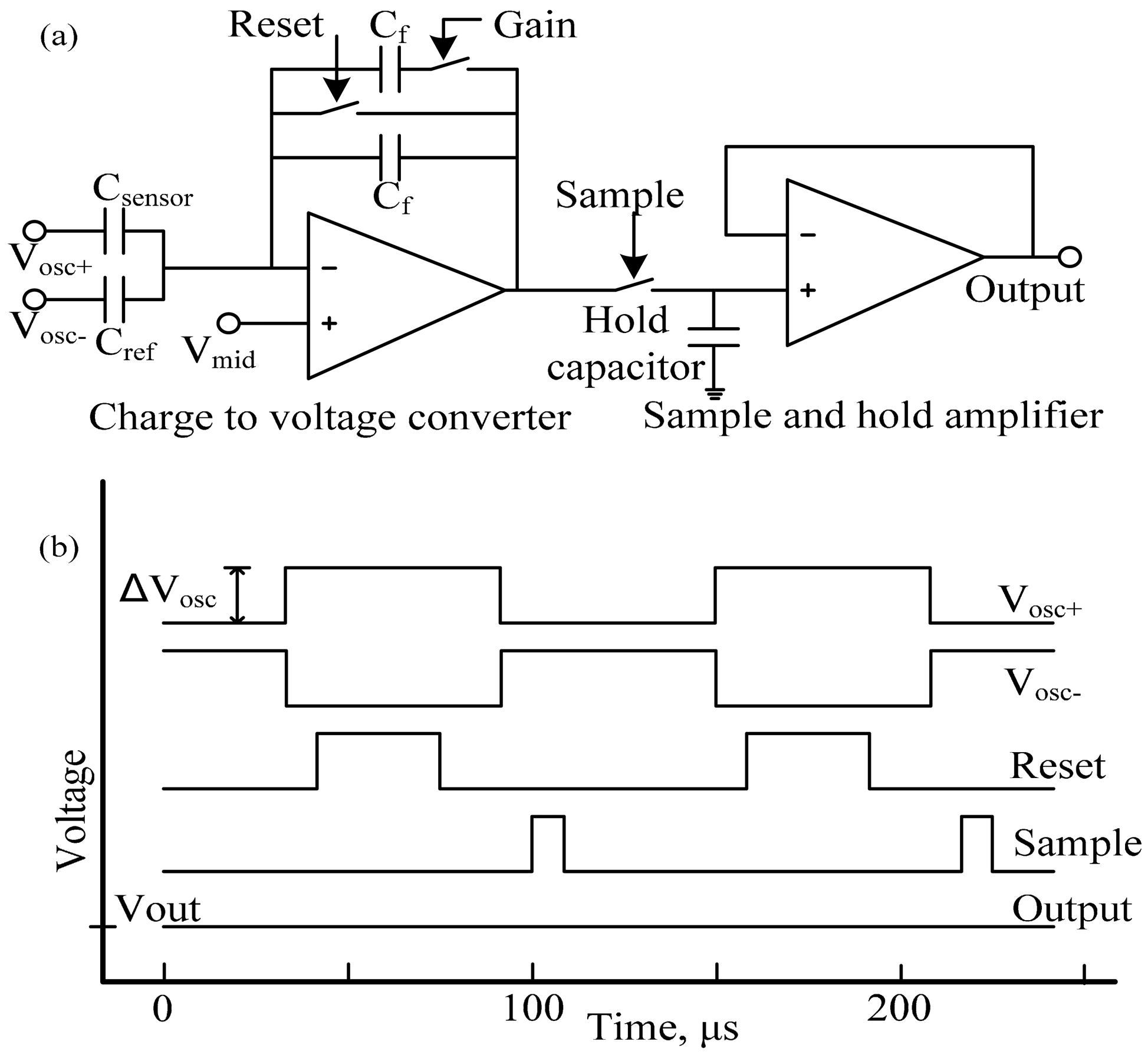
Figure 1a illustrates the schematic diagram of the differential wide temperature CMOS interface circuit for capacitive MEMS pressure sensors. The circuit uses a switched capacitor technique and a similar circuit has been used previously by our group [13] for MEMS air flow sensors and by Patel et al. [14] towards chemocapacitive sensing of volatile organic compounds. Here, we use a novel differential input circuit that enables working with MEMS sensors that have a wide range of the steady-state capacitance values from 0.5 pF to 10 pF. The circuit measures the capacitance of external sensor, Csensor, and produces an analog output voltage, Vout. A reference capacitor, Cref is needed that has a similar steady-state capacitance value as the sensor device, Csensor, to extend the detection dynamic range while providing good capacitance detection resolution required for MEMS pressure sensors.
In operation, two 10 kHz square wave signals VOSC+ and VOSC− with same amplitude but opposite phase are used to drive the sensor capacitor, Csensor and reference capacitor, Cref. Their amplitude is defined as ΔVosc. Vmid is a DC voltage applied to the non-inverting node of the amplifier. Reset, Sample and Gain are control signals where the Gain switch can adjust the feedback capacitance in the circuit, Cfedback, to be either Cf or 2Cf. In the present design, the values of Cf and the hold capacitor, CH are both set as 1 pF. The waveforms of the control and output signals for the converter circuit are shown in Figure 1b. The amplitude of the output voltage can be expressed as Equation (1),
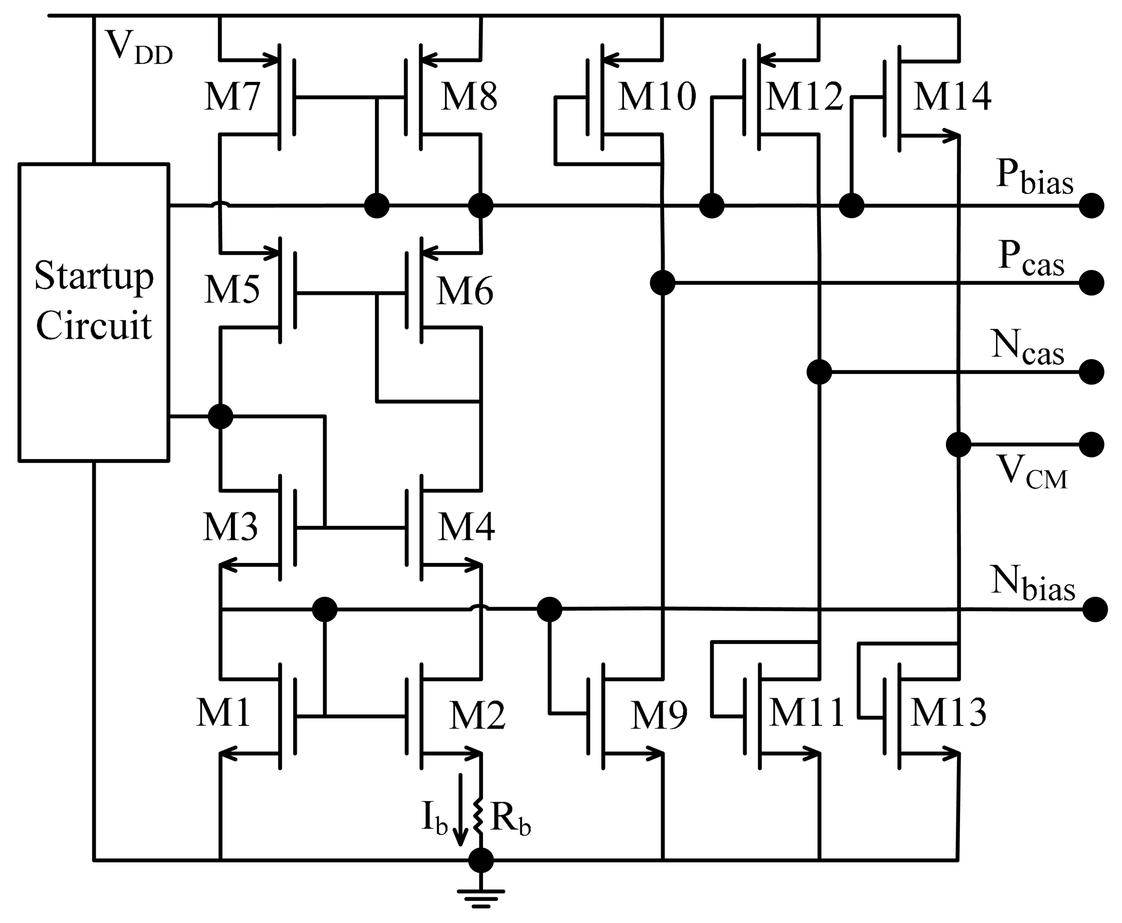
At high temperatures, the overall performance of operational amplifiers implemented in CMOS process degrade greatly, most notably by showing loss of open loop gain and decrease of bandwidth. Effective design techniques are required to compensate high temperature effects and reduce the impact of excessive leakage current [9,15,16] Amongst different high temperature compensation techniques, the constant-gm biasing technique is a popular choice which has been proven effective over the wide temperature range [17,18]. A biasing circuit using constant-gm biasing technique is shown in Figure 2. When neglecting channel length modulation and the body effect, the gm of a transistor biased by current, Ib as shown in Figure 2 can be expressed as Equation (2),
As can be seen, the gm of the transistor is inversely proportional to the biasing resistor, Rb. Ideally, if Rb has a zero Temperature Coefficient (TC), then gm will be constant as the temperature changes. The IBM 0.13 μm CMOS technology offers a resistor with TC around 100 ppm/°C. The biasing circuit when implemented with this resistor can achieve considerably high stability over a wide temperature range. A folded-cascode amplifier with a switched-capacitor common-mode feedback (CMFB) circuit is used as the amplifier in Figure 1a [13]. A constant-gm biasing circuit is used to bias the amplifier to stabilize the amplifier performance (open loop gain and bandwidth) over the wide temperature range. As the open loop gain decreases when temperature increases, a higher gain amplifier is necessary, such that it still maintains sufficient gain at high temperatures. A NMOS input pair is used in our design to attain large gain while keeping the device sizes reasonably small.
For the chip layout, common-centroid structures are used wherever applicable to reduce temperature induced common mode errors. Guard rings are placed around performance sensitive blocks to prevent latch-up at high temperatures.
3. Experimental Results and Discussion
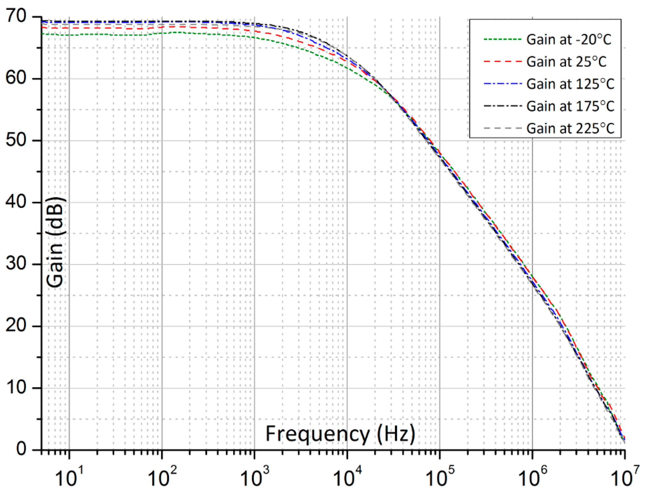
The CMOS sensor interface circuit is fabricated using the IBM 0.13 μm CMOS process available through the Canada Microelectronics Corporation. The microphotograph of the fabricated chip is shown in the inset of Figure 3a. The chip is placed under the nozzle of a thermal inducing system (Thermostream TP04100A, Temptronic Corp., Mansfield, MA, USA), where the chip temperature can be varied from −20 °C to 225 °C, which is the temperature limit of the Thermostream testing system as shown in Figure 3b. The temperature under the nozzle is monitored using a thermocouple and the temperature accuracy is better than ±1 °C. Figure 4 shows the measured single-ended open-loop gain of the amplifier driving 2 pF load capacitance at different temperatures. From −20 °C to 225 °C, the measured DC gain varies by only 2.1 dB. The measured amplifier power consumption (including constant-gm biasing circuit) at 225 °C is 0.51 mW. We tested three out of five received packed chips and all showed similar frequency response versus temperatures.
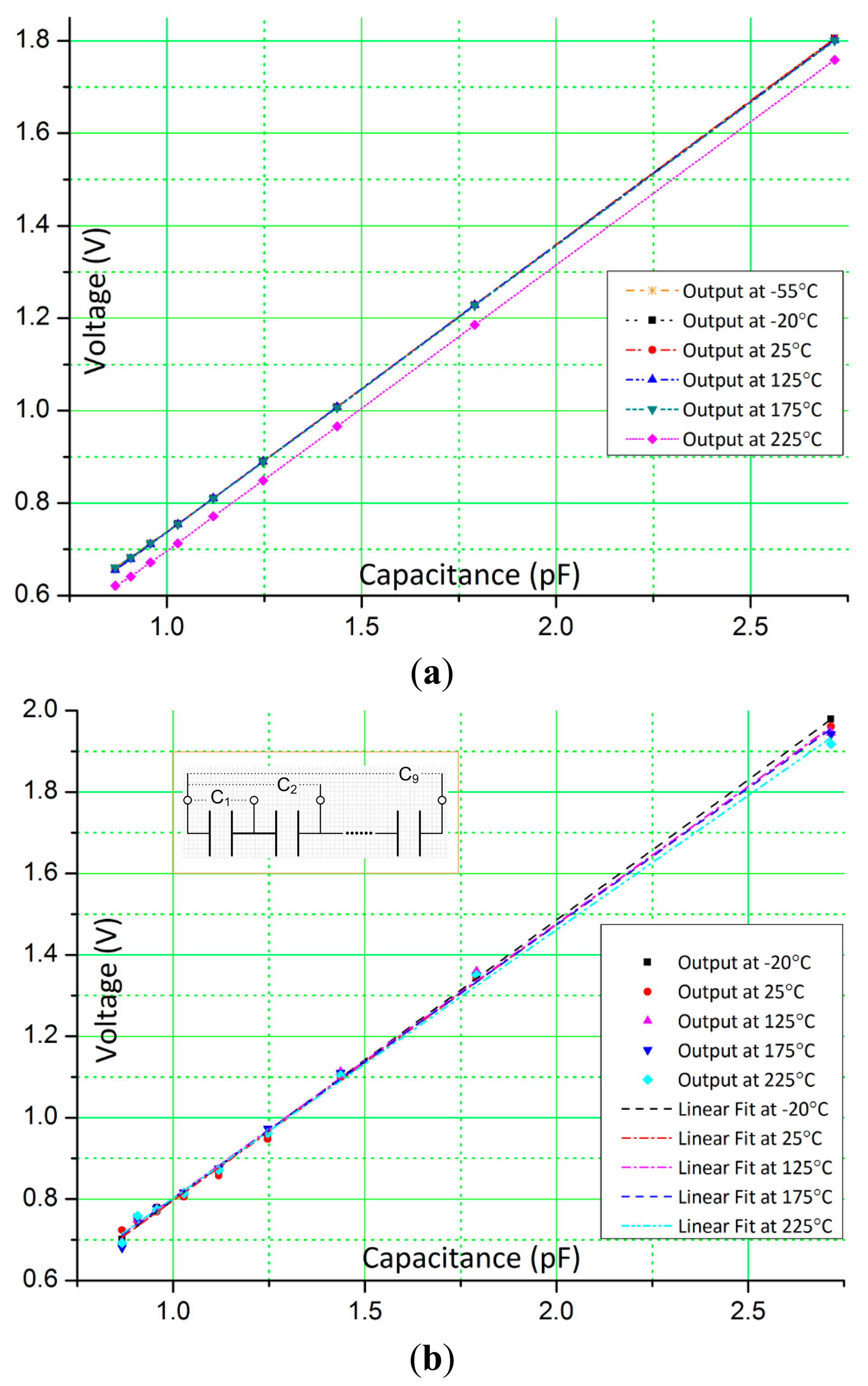
Figure 5a,b show the output voltages for different capacitance values during calibration at temperature ranges, simulated from −55 °C to 225 °C and measured from −20 °C to 225 °C. Again, the measured temperature range is less due to the limit of the Thermostream testing system. Generally, colder temperatures between −55 °C and −20 °C do not have detrimental effects on CMOS electronics and further help to improve signal to noise ratio due to reduced noise effects. The calibration capacitance, Csensor, is constructed by using nine capacitors, C1 to C9 (shown in inset of Figure 5b) with nominal capacitance value of 1 pF which are connected in series. By appropriately changing connections from C1 to C9, the capacitance value of Csensor is varied and measured using a high resolution universal capacitance readout circuit, MS3110 (MicroSensors, Costa Mesa, CA, USA) that is maintained at room temperature (25 °C).
The control signals, Vosc+, Vosc−, Reset and Sample are generated by a data acquisition card, NI USB-6259 (National Instruments Inc., Austin, TX, USA). The amplitude of Vosc is set to 1.25 V, Vmid is set to analog ground 1.25 V, the feedback capacitance, Cf is set to 2 pF, and the reference capacitance, Cref is fixed to 1.805 pF. The sensor capacitor, Csensor, and reference capacitor, Cref, are placed at room temperature (25 °C) with only the test chip which includes the on-chip feedback capacitor Cf exposed to the temperature change from −20 °C to 225 °C. From Figure 5, the measured results show similar response as simulated results. Over the wide temperature range, the circuit converts the input capacitance to output voltage with goodness-of-fit of linear regression of 0.998 (R2). Figure 6 shows the difference between the measured results and the linear fits, which is defined as, (measured value-fitted value)/(fitted value). The overall difference is around 2%, and larger difference is observed when the sensor capacitance is smaller and at high temperatures. The tested linearity is worse than the simulated results, especially when the capacitance is smaller and its probable cause could be interconnect parasitic capacitance in the experimental setup.
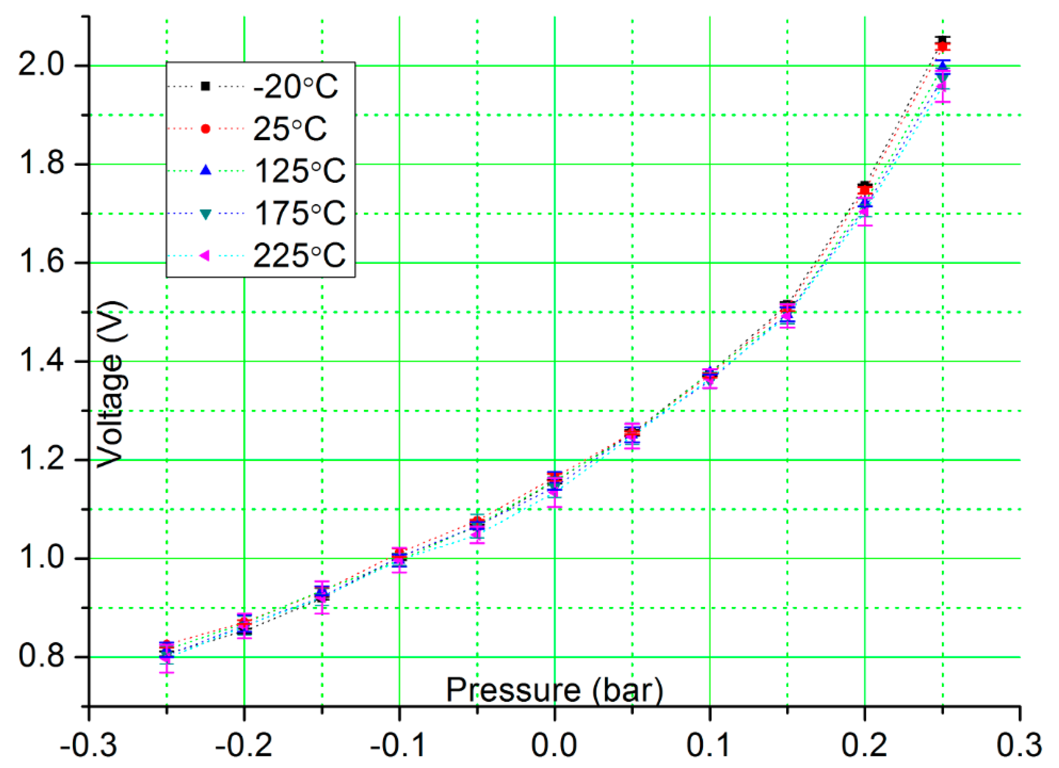
The CMOS circuit is interfaced with a capacitive MEMS pressure sensor from Protron Mikrotechnik GmbH, Germany [19] by replacing the Csensor with the pressure sensor in Figure 1. The feedback capacitance, Cf is set to 2 pF. The sensor operates within a temperature range from −40 °C to +85 °C with a sensitivity of 1 fF/mbar. During our experimental testing, the MEMS pressure sensor is maintained at room temperature (25 °C) and placed in a pressure vessel so that its capacitance output does not change with ambient temperature and only varies when external pressure is applied to the pressure vessel. Figure 7 shows the measured output voltage to pressure change when the CMOS sensor interface circuit is exposed to temperature range from −20 °C to 225 °C. The MEMS pressure sensor is exposed to pressure variation from −0.25 bar to +0.25 bar. All measurements are done in triplicate with the average value noted in Figure 7. As can be seen, the output voltage from the CMOS circuit changes in accordance with the capacitance change of the pressure sensor and provides a stable response over a temperature range from −20 °C to 225 °C. The estimated sensor readout resolution is 2.322 mV/mbar at 225 °C. As temperature increases, the output noise becomes larger. The simulated noise analysis shows the noise level at the output of the circuit in Figure 1a increases from 0.134 mVHz−1/2 to 0.184 mVHz−1/2 when temperatures changes from −55 °C to 125 °C. Another major error source at high temperatures is the leakage current in the Sample switch, which can cause a voltage drop or rise on the hold capacitor, depending on the direction of the leakage current. This problem can be alleviated using higher sampling speed, or increasing the capacitance of the hold capacitor. A sample/hold circuit with dynamic switch leakage compensation [20] can also be used, with the penalty of increased circuit complexity.
In our experiments, the temperature for the sensor and reference capacitors is fixed at 25 °C. In real world applications, the sensor capacitor and reference capacitors will also undergo wide temperature change. The sensor capacitor and reference capacitor are often identical and they usually have the same TCs, around 100 ppm/°C. The TC of the on-chip feedback capacitor is about 13 ppm/°C according to the IBM 0.13 μm CMOS process design manual. According to Equation (1), some errors could be introduced due to the TC difference. The sensor capacitance, Csensor is comprised of a steady-state capacitance defined as C0 and a capacitance change during operation defined as, ΔC. And the reference capacitance, Cref is usually about the same value of C0. Now Equation (1) can be written as:
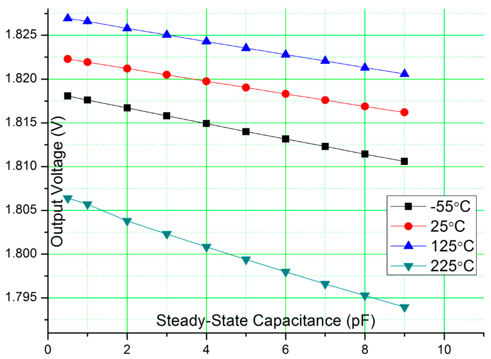
As can be seen, due to the differential readout scheme, the C0 component is cancelled and only ΔC is considered. Figure 8 shows the simulated output voltage for different steady-state capacitance from −55 °C to 225 °C. The TCs of sensor capacitor and reference capacitor are set to 100 ppm/°C. ΔC is set to 0.5 pF at 25 °C, Vmid and ΔVosc are set to 1.25 V, and Cfeedback is set to 1 pF. As can be seen, when the steady-state capacitance changes from 0.5 pF to 10 pF, the output voltages decrease only about 20 mV. This shows the circuit has good flexibility to interface with MEMS sensors with a wide range of the steady-state capacitance values. At a fixed steady-state capacitance, the output voltages change by less than 30 mV when temperature varies from −55 °C to 225 °C. This means the TC difference has very limited impact to the interface circuit. For MEMS sensors which do not have a reference capacitor, low TC mica capacitor (with TC about 50 ppm/°C) can be used as reference capacitor.
4. Conclusions
A CMOS differential interface circuit for capacitive MEMS pressure sensors is designed, fabricated and tested that is functional over a wide temperature range between −55 °C and 225 °C. The circuit is implemented using IBM 0.13 μm CMOS technology with 2.5 V power supply. Experimental results show that the circuitry has excellent temperature stability and an overall linearity error of around 2% over the wide temperature range with goodness-of-fit of linear regression of 0.998 (R2). The circuit was tested using a commercial capacitive MEMS pressure sensor and provided a stable response over the wide temperature range.
Acknowledgments
We would like to thank the financial support provided by NSERC to Chodavarapu and Wang and MEDA Fellowship to Wang. We would like to thank Canada Microelectronic Corporation for providing access to the CMOS fabrication service.
Author Contributions
Y.W. conducted the research presented in the article. Y.W. and V.C. contributed towards writing of the article.
Conflicts of Interest
The authors declare no conflict of interest.
References
- Beeby, S. MEMS Mechanical Sensors; Artech House: Boston, MA, USA, 2004. [Google Scholar]
- Esashi, M. Revolution of Sensors in Micro-Electromechanical Systems. Jpn. J Appl. Phys. 2012, 51. [Google Scholar] [CrossRef]
- Eaton, W.P.; Smith, J.H. Micromachined pressure sensors: Review and recent developments. Proceedings of SPIE3046, Smart Structures and Materials 1997: Smart Electronics and MEMS, San Diego, CA, USA, 19 June 1997.
- Wise, K.D. Integrated sensors, MEMS, and microsystems: Reflections on a fantastic voyage. Sens. Actuators A Phys. 2007, 136, 39–50. [Google Scholar]
- Capatitance to digital converters. Available online; http://www.analog.com/en/analog-to-digital-converters/capacitance-to-digital-converters/products/index.html#Capacitive_to_Digital_Converters (accessed on 9 February 2015).
- Hunter, G.W.; Neudeck, P.G.; Okojie, R.S.; Beheim, G.M.; Powell, J.; Chen, L. An overview of high-temperature electronics and sensor development at NASA Glenn Research Center. J. Turbomach. 2003, 125, 658–664. [Google Scholar]
- Barlian, A.A.; Park, W.-T.; Mallon, J.R.; Rastegar, A.J.; Pruitt, B.L. Review: Semiconductor piezoresistance for microsystems. IEEE Proc. 2009, 97, 513–552. [Google Scholar]
- Hezarjaribi, Y.; Hamidon, M.; Keshmiri, S.; Bahadorimehr, A. Capacitive Pressure Sensors Based on MEMS, Operating in Harsh Environments. Proceedings of the 2008 ICSE 2008 IEEE International Conference on Semiconductor Electronics, Johor Bahru, Malaysia, 25–27 November 2008; IEEE: Piscataway, NJ, USA, 2008. [Google Scholar]
- Baccar, S.; Levi, T.; Dallet, D.; Shitikov, V.; Barbara, F. Modeling Methodology for Analog Front-End Circuits Dedicated to High-Temperature Instrumentation and Measurement Applications. IEEE Trans. Instrum. Meas. 2011, 60, 1555–1564. [Google Scholar]
- De Jong, P.C.; Meijer, G.C. A high-temperature electronic system for pressure-transducers. IEEE Trans. Instrum. Meas. 2000, 49, 365–70. [Google Scholar]
- Levinzon, F.A. 175 Silicon-Based Hybrid Charge Amplifier for 175 and 100-mV/G Miniature Piezoelectric Accelerometer. IEEE Sens. J. 2006, 6, 1164–1169. [Google Scholar]
- Sadeghi, N.; Mirabbasi, S.; Bennington, C.P. A 2.5 V, 0.13 μm CMOS Amplifier for a High-Temperature Sensor System. Proceedings of the 2009 NEWCAS-TAISA’09 Joint IEEE North-East Workshop on Circuits and Systems and TAISA Conference, Toulouse, France, 28 June– 1 July 2009; IEEE: Piscataway, NJ, USA, 2009. [Google Scholar]
- Merdassi, A.; Wang, Y.; Xereas, G.; Chodavarapu, V.P. Design and fabrication of a three-axis accelerometer sensor microsystem for wide temperature range applications using semi-custom process. Proceedings of the SPIE MOEMS-MEMS Conference, San Fransisco, CA, USA, 3–5 March 2014.
- Patel, S.; Mlsna, T.; Fruhberger, B.; Klaassen, E.; Cemalovic, S.; Baselt, D. Chemicapacitive microsensors for volatile organic compound detection. Sens. Actuators B Chem. 2003, 96, 541–553. [Google Scholar]
- De Jong, P.C.; Meijer, G.C.; van Roermund, A.H. A 300 C dynamic-feedback instrumentation amplifier. IEEE J. Solid-State Circuits 1998, 33, 1999–2009. [Google Scholar]
- Haslett, J.; Trofimenkoff, F.; Finvers, I.; Sabouri, F.; Smallwood, R. High Temperature Electronics Using Silicon Technology. Proceedings of the 1996 IEEE International Solid-State Circuits Conference, 1996 Digest of Technical Papers 42nd ISSCC, San Francisco, CA, USA, 10 February 1996; IEEE: Piscataway, NJ, USA, 1996. [Google Scholar]
- Yu, X.; Garverick, S.L. A 300 °C, 110-dB σ-δ Modulator with Programmable Gain in Bulk CMOS. Proceedings of the 2006 CICC’06 IEEE Custom Integrated Circuits Conference, San Jose, CA, USA, 10–13 September 2006; IEEE: Piscataway, NJ, USA, 2006. [Google Scholar]
- Majerus, S.; Merrill, W.; Garverick, S.L. Design and long-term operation of high-temperature, bulk-CMOS integrated circuits for instrumentation and control. Proceedings of the 2013 IEEE Energytech, Cleveland, OH, USA, 21–23 May 2013; pp. 1–6.
- Available online: http://www.protron-mikrotechnik.de/download/Protron-Pressure-Sensor-11_2014.pdf (accessed on 9 February 2015).
- Zou, L.; Pathrose, J.; Chai, K.; Je, M.; Xu, Y. Sample-and-hold circuit with dynamic switch leakage compensation. Electron. Lett. 2013, 49, 1323–1325. [Google Scholar]


© 2015 by the authors; licensee MDPI, Basel, Switzerland. This article is an open access article distributed under the terms and conditions of the Creative Commons Attribution license ( http://creativecommons.org/licenses/by/4.0/).
Share and Cite
Wang, Y.; Chodavarapu, V.P. Differential Wide Temperature Range CMOS Interface Circuit for Capacitive MEMS Pressure Sensors. Sensors 2015, 15, 4253-4263. https://doi.org/10.3390/s150204253
Wang Y, Chodavarapu VP. Differential Wide Temperature Range CMOS Interface Circuit for Capacitive MEMS Pressure Sensors. Sensors. 2015; 15(2):4253-4263. https://doi.org/10.3390/s150204253
Chicago/Turabian StyleWang, Yucai, and Vamsy P. Chodavarapu. 2015. "Differential Wide Temperature Range CMOS Interface Circuit for Capacitive MEMS Pressure Sensors" Sensors 15, no. 2: 4253-4263. https://doi.org/10.3390/s150204253
APA StyleWang, Y., & Chodavarapu, V. P. (2015). Differential Wide Temperature Range CMOS Interface Circuit for Capacitive MEMS Pressure Sensors. Sensors, 15(2), 4253-4263. https://doi.org/10.3390/s150204253