A Single-Walled Carbon Nanotube Network Gas Sensing Device

 ,
, 
Abstract
: The goal of this research was to develop a chemical gas sensing device based on single-walled carbon nanotube (SWCNT) networks. The SWCNT networks are synthesized on Al2O3-deposted SiO2/Si substrates with 10 nm-thick Fe as the catalyst precursor layer using microwave plasma chemical vapor deposition (MPCVD). The development of interconnected SWCNT networks can be exploited to recognize the identities of different chemical gases by the strength of their particular surface adsorptive and desorptive responses to various types of chemical vapors. The physical responses on the surface of the SWCNT networks cause superficial changes in the electric charge that can be converted into electronic signals for identification. In this study, we tested NO2 and NH3 vapors at ppm levels at room temperature with our self-made gas sensing device, which was able to obtain responses to sensitivity changes with a concentration of 10 ppm for NO2 and 24 ppm for NH3.1. Introduction
Carbon nanotubes (CNTs) are molecular scale quantum wires exhibiting many unique properties for potential nano-devices applications [1–6]. One of the applications is as the sensing materials in a gas sensor device. Single-walled carbon nanotubes (SWCNTs), multi-walled CNTs (MWCNTs) and randomly oriented nanotube networks for detecting chemical gases and vapors have been a subject of active research [7–10]. Some devices were designed to detect the changes in the resistance of the Schottky barriers among the nanotubes and their metal contacts [11], which could be used to improve the real-time sensing to monitor the combustible gases, gas leakage and environmental pollution. However, a few studies have shown the main disadvantages of this kind of gas sensor, which include operating at a high temperature, requiring higher conductivities, and needing a clean sensing chamber.
In this study, we demonstrate the simple and rapid manipulation of carbon nanotube materials using direct growth manipulation to build a practical nano-device. These CNT-assisted sensor devices also showed excellent sensitivity and a rapid response time to detect NO2 and NH3 with the aim of obtaining the sensor’s detection limit by observing the changes in electric resistance.
2. Experiment
2.1. Growth of SWCNT Networks
The SWCNT networks used in this work were grown by a MPCVD system. The synthesis process has been described elsewhere in detail [12,13]. In brief, an Al2O3 layer of 10 nm was first deposited on SiO2/Si wafer substrates, followed by an iron (Fe) film with a thickness of 10 nm. The SWCNT networks were grown on the substrates using a microwave plasma at a power of 750 W in a chamber pressure of 12 Torr under constant gas flows of H2 (400 sccm) and CH4 (1.5 sccm) for 10 min. The substrate temperature was estimated to be ∼650 °C during the growth of the SWCNT networks. Prior to the deposition process, the Fe/Al2O3-coated samples were pretreated by 30 Torr hydrogen plasma under the condition of a 100 sccm H2 gas flow rate with an input microwave power of 600 W for 15 min. The grown products were characterized by field emission scanning electron microscopy (FESEM, JEOL-6500), high resolution transmission electron microscopy (HRTEM, JEM-2100F), and micro-Raman spectroscopy (Renishaw RM-1000, excitation laser: 514.5 nm in wavelength, laser spot: ∼5 μm in diameter).
2.2. Gas Sensing Setup and Measurement
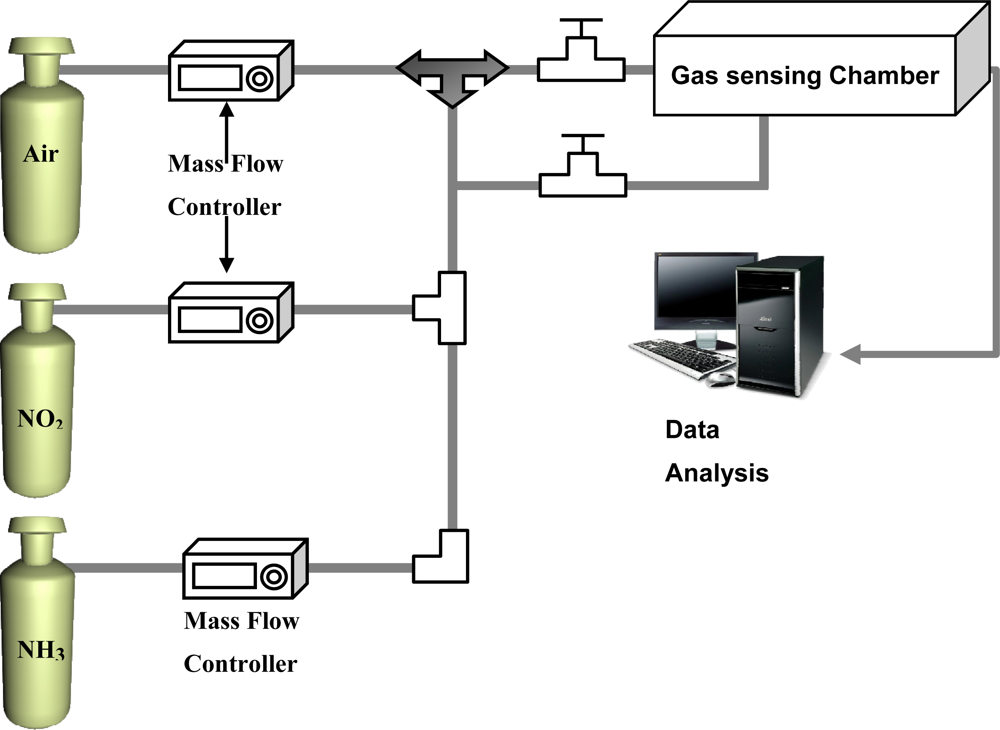
The gas sensing devices were prepared by directly soldering the two electrical leads in an air atmosphere on the surface of the SWCNT networks deposited on the SiO2/Si substrates. The distance between the two electrodes was 1 cm. Figure 1 shows the experimental setup used in the measurements. For safety, the experiments were conducted under a hood. The sensor device was placed inside the gas sensing chamber with 0.1 L capacity. Dry air was used as background gas and the flow rate was set at 100 sccm. The concentration of NO2 and NH3 gas were controlled by mass flow controller. For gas sensing, the reaction chamber was alternately purged by the dried-and-filtered air and testing gas, respectively, with a duration time of 30 s for each under a flow rate of 100 sccm. The resistance between the two electrodes on the SWCNT networks as a function of purging time was recorded every second by a computer interfaced with an electrical resistance meter through a GPIB bus.
3. Experimental Results and Discussion
3.1. Surface Morphology and Microstructure of SWCNT Networks as Gas Sensing Materials
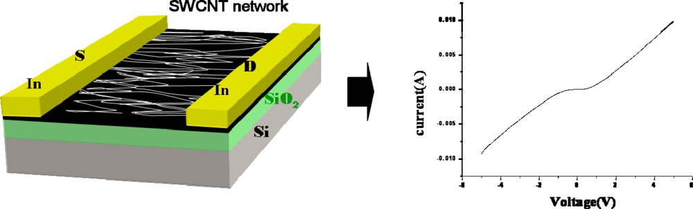
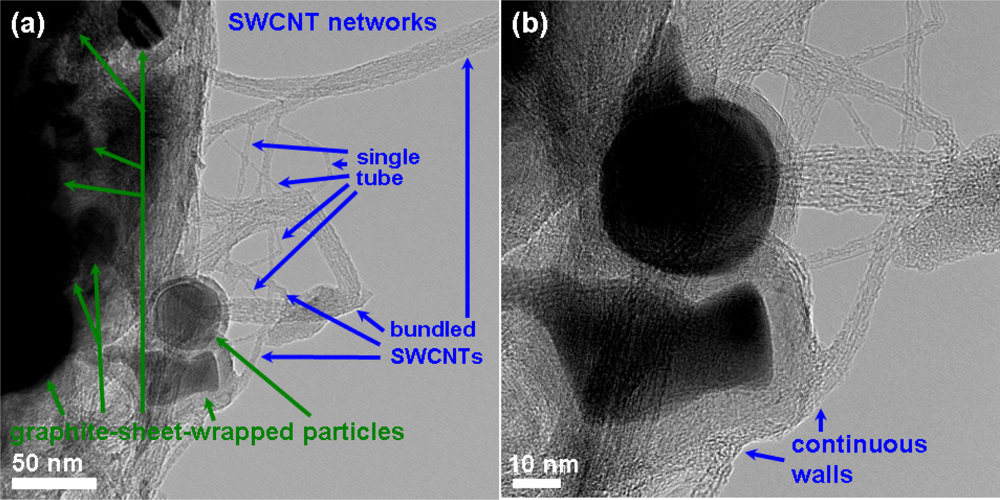
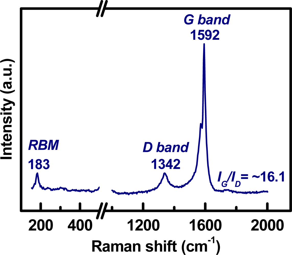
Figure 2 shows the SEM micrograph of the as-grown CNT networks on an Al2O3-deposited SiO2/Si substrate. It can be observed that the CNTs are surface-grown and connected to each other between catalyst particles, forming a laterally interconnected network. To examine the structure of the CNTs, the developed CNT networks are further characterized by HRTEM after being ultrasonically dispersed on a carbon grid. A low magnification HRTEM image, as shown in Figure 3(a), reveals that the CNT-based lateral architecture comprises a mixture of graphene-sheet-wrapped catalyst particles and interconnected SWCNTs, alone or assembled into bundles. Moreover, the HRTEM image shown in Figure 3(b) at high magnification further shows that the walls of the SWCNTs connect continuously with the outer layer of the graphitic shells of the given particles. Moreover, to evaluate the structural properties of the prepared SWCNT networks, we also employed Raman scattering, which is one of the most widely used and powerful techniques to characterize CNT samples. Figure 4 shows the Raman spectrum characteristics of our SWCNT networks. The existence of highly-graphitized SWCNTs can be confirmed by a high fitted-peak area ratio of the G-band to the D-band, namely IG/ID, and the radial breathing modes (RBM) peaks in the low frequency region of 100–300 cm−1. The strong signal at about 1,592 cm−1 is attributed to the G-band of the tangential mode of a graphite-like material while the peak around 1,342 cm−1 is the D-band representing defects in the graphite structures. It is clear that the IG/ID ratio is approximately 16.1 for our sample, indicating the growth of highly crystallized SWCNTs in the networks. In addition, the strong RBM peak at around 183 cm−1 implies that the majority of tubes are about 1.35 nm in diameter in the resonant case when using the 514.5 nm line of the Ar laser for excitation [14–16]. Figure 5 provides a schematic diagram and I-V curve of the device. The source (S) and drain (D) Indium electrodes were added to this substrate with SWCNTs networks by using low temperature bonding techniques. This makes the process easier for mass production, comparing to the existing CNTFET that needs semiconductor post-fabrication process for electrode making and device packaging.
3.2. Gas Sensing Performance
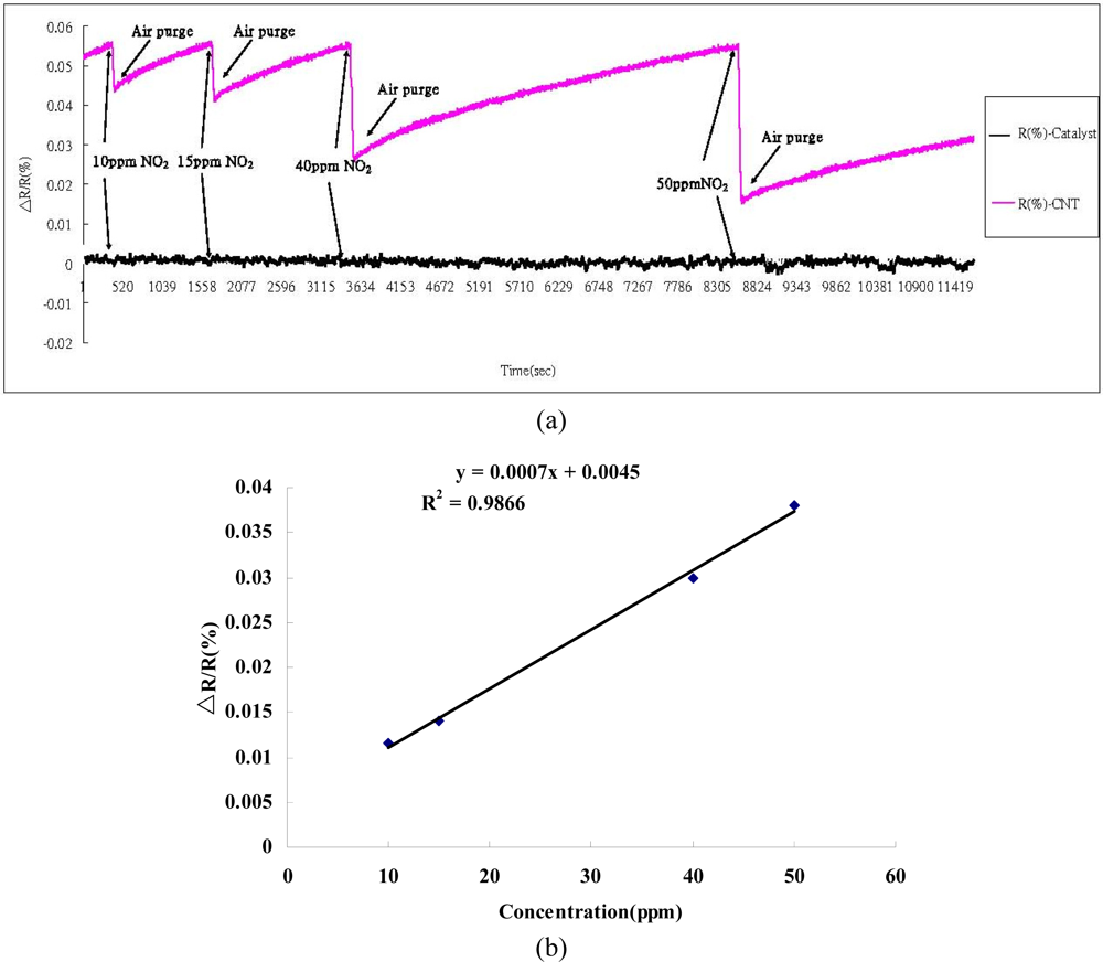
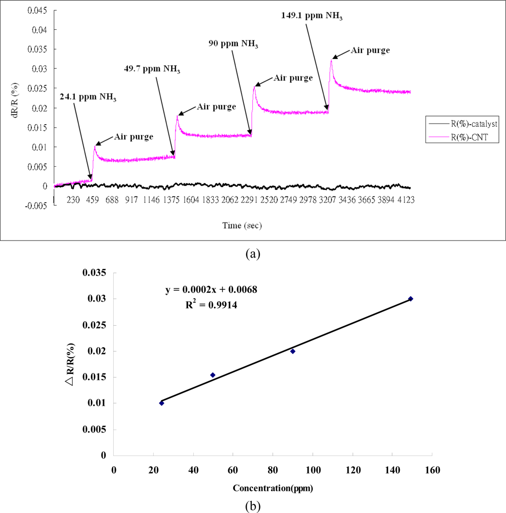
To investigate the responses of the SWCNT networks to gaseous toxic chemicals by measuring the changes in resistance, NO2 and NH3 gases were used in the experiments. It was obvious that the value of the resistance dropped upon binding of the NO2 or NH3 molecules [17–20]. This could result in the transfer of electrons from CNTs to NO2 molecules, which are strong oxidants bearing an unpaired electron, and thus could lead to a decrease in the resistance of the CNTs when NO2 is bound to the surface of semiconducting CNTs (Figure 6). The response to NO2 isn't clear because the recovery time is very long. The high bonding energy between SWCNTs and NO2 results in our gas sensing devices not reaching saturation during the designed analyte gas exposure time (30 s). This long recovery time has also been reported for carbon nanotube sensors by Kong et al. [17]. However, the binding of the NH3 gas was observed to cause an elevation in resistance. This may be attributable to the absorption of reductive NH3 molecules to the surface of carbon nanotubes, leading to electrons being transferred from NH3 molecules to the CNTs’ valence bands (Figure 7) [17,21]. Based on the obtained data, it appears that the influence of gas adsorption on the SWCNTs varied with different gas species, and the self-developed SWCNT networks possessed outstanding sensitivity with semiconducting traits [22,23].
In addition, the larger the superficial measurement is, the more test gas is needed. In the experiment, we concluded that test gases at low ppm levels could lead to low responses from the sensing device. To obtain better responses from the SWCNT networks with a low ppm or even ppb levels, the sensing device would need to be reduced in size [24]. In the test of NH3, we found the sensors behaved well when compared to other results [18,20]. There is a constant drift due to an irreversible gas sensing process, which might be due to chemisorption between the defect along the sidewall and the NH3 molecules, as reported by Robinson et al. [25].
It is well known that both semiconducting and metallic tubes are products of all SWCNTs synthesis methods. The metallic SWCNTs may be burned off after fabrication [26], but this additional processing step makes it more difficult for control and mass production. Bao’s results [27,28] showed that semiconducting and metallic SWCNTs could be separated by using different functionalized surfaces and produces TFT device sensor presented very good device characteristics. The TFT sensors fabricated with aligned, sorted nanotube networks (enriched with semiconductor SWCNTs) showed a higher sensitivity to analytes than those fabricated with random, unsorted networks with predominantly metallic charge transport.
Our gas sensing device fabrication process directly grows the SWCNT networks on the surface of device without using any chemical solution. As a result, the sensing materials on the gas sensing device should be a combination of both semiconducting and metallic tubes. It behaves like a chemiresister sensor. These SWCNTs chemiresistor sensors operate by a change in conductance due to a relatively stronger charge transfer interaction, as opposed to weaker dipole or van der Waals interactions. Consequently, our gas sensing device does not need an additional process to burn off the metallic SWCNTs after fabrication, and functions as a chemiresistor.
These SWCNTs chemiresistor sensors operate by a change in conductance due to a relatively stronger charge transfer interaction, as opposed to weaker dipole or Van der Waals interactions. Carbon nanotubes provide a large surface area for gases passing through such that the sensitivity of gas sensing is greatly enhanced. Therefore, carbon nanotubes are proven to be highly sensitive for detection of low concentration gas molecules. The main detection principle is the charge exchange between SWCNT sidewalls and gas molecules absorbed by the surface of carbon nanotubes. The molecular interactions with defect sites in SWCNT sidewalls strongly affect their electrical response. In our experiments, NO2 are electron withdrawing molecules, while NH3 are electron donating molecules.
4. Conclusions and Future Work
We have demonstrated the use of a gas-sensing material based on SWCNT networks and investigated the influence of various concentrations of NH3 and NO2 gases within the SWCNT networks in terms of the performance in detecting NH3 and NO2. The proposed gas sensing device does not need an additional processing step to burn off the metallic SWCNTs after fabrication. This makes the process easier to implement for mass production. In addition, the proposed sensing device functions as a chemiresistor. Source (S) and drain (D) indium electrodes were added to this substrate with SWCNTs networks by using low temperature bonding techniques. This again makes the process more practical for mass production, compared to the existing CNTFET that needs a semiconductor post-fabrication process for electrode making and device packaging. The main improvement was to modify the nanomaterial to increase the compatibility between the two components; therefore, the SWCNT networks can be easily fabricated in the gas sensing material. These would also help us to realize the gas sensing performance of the SWCNT networks materials without using any chemical solution on it.
Acknowledgments
The authors would like to acknowledge the support of the National Science Council of Taiwan, under Project No. NSC100-2220-E-007-008, No. NSC98-2221-E-451-001 and NSC97-2112-M-214-002-MY2. We also thank the CSIST for supporting us with the use of the gas sensing instrument in this research.
References
- Dekker, C. 1999, 52, 22–30.
- Collins, PG; Bradley, K; Ishigami, M; Zettl, A. Extreme oxygen sensitivity of electronic properties of carbon nanotubes. Science 2000, 287, 1801–1804. [Google Scholar]
- Romero, H; Sumanasekera, G; Mahan, G; Eklund, P. Thermoelectric power of single-walled carbon nanotube films. Phys Rev B 2002, 65, 205410:1–205410:6. [Google Scholar]
- Derycke, V; Martel, R; Appenzeller, J; Avouris, P. Controlling doping and carrier injection in carbon nanotube transistors. Appl. Phys. Lett 2002, 80, 2773–2775. [Google Scholar]
- Rosenblatt, S; Yaish, Y; Park, J; Gore, J; Sazonova, V; McEuen, PL. High performance electrolyte gated carbon nanotube transistors. Nano Lett 2002, 2, 869–872. [Google Scholar]
- Postma, HWC; Teepen, T; Yao, Z; Grifoni, M; Dekker, C. Carbon nanotube single-electron transistors at room temperature. Science 2001, 293, 76–79. [Google Scholar]
- Snow, E; Perkins, F; Houser, E; Badescu, S; Reinecke, T. Chemical detection with a single-walled carbon nanotube capacitor. Science 2005, 307, 1942–1945. [Google Scholar]
- Chopra, S; Pham, A; Gaillard, J; Parker, A; Rao, A. Carbon-nanotube-based resonant-circuit sensor for ammonia. Appl. Phys. Lett 2002, 80, 4632–4634. [Google Scholar]
- Someya, T; Small, J; Kim, P; Nuckolls, C; Yardley, JT. Alcohol vapor sensors based on single-walled carbon nanotube field effect transistors. Nano Lett 2003, 3, 877–881. [Google Scholar]
- Snow, E; Novak, J; Campbell, P; Park, D. Random networks of carbon nanotubes as an electronic material. Appl. Phys. Lett 2003, 82, 2145–2147. [Google Scholar]
- Suehiro, J; Imakiire, H; Hidaka, S; Ding, W; Zhou, G; Imasaka, K; Hara, M. Schottky-type response of carbon nanotube NO2 gas sensor fabricated onto aluminum electrodes by dielectrophoresis. Sens. Actuat. B: Chem 2006, 114, 943–949. [Google Scholar]
- Wang, W; Peng, Y; Kuo, C. Effects of buffer layer materials and process conditions on growth mechanisms of forming networks of SWNTs by microwave plasma chemical vapor deposition. Diam. Relat. Mat 2005, 14, 1906–1910. [Google Scholar]
- Teng, I. Highly graphitized laterally interconnected SWCNT network synthesis via a sandwich-grown method. J Phys D Appl Phys 2011. [Google Scholar] [CrossRef]
- Jorio, A; Pimenta, MA; Souza Filho, AG; Saito, R; Dresselhaus, G; Dresselhaus, MS. Characterizing carbon nanotube samples with resonance Raman scattering. New J Phys 2003. [Google Scholar] [CrossRef]
- Dresselhaus, M; Dresselhaus, G; Jorio, A; Souza Filho, A; Saito, R. Raman spectroscopy on isolated single wall carbon nanotubes. Carbon 2002, 40, 2043–2061. [Google Scholar]
- Dresselhaus, MS; Dresselhaus, G; Saito, R; Jorio, A. Raman spectroscopy of carbon nanotubes. Phys. Reports 2005, 409, 47–99. [Google Scholar]
- Kong, J; Franklin, NR; Zhou, CW; Chapline, MG; Peng, S; Cho, KJ; Dai, HJ. Nanotube molecular wires as chemical sensors. Science 2000, 287, 622–625. [Google Scholar]
- Peng, N; Zhang, Q; Lee, YC; Tan, OK; Marzari, N. Gate modulation in carbon nanotube field effect transistors-based NH3 gas sensors. Sens. Actuat. B: Chem 2008, 132, 191–195. [Google Scholar]
- Li, J; Lu, Y; Ye, Q; Cinke, M; Han, J; Meyyappan, M. Carbon nanotube sensors for gas and organic vapor detection. Nano Lett 2003, 3, 929–933. [Google Scholar]
- Villalpando-Paez, F; Romero, A; Munoz-Sandoval, E; Martinez, L; Terrones, H; Terrones, M. Fabrication of vapor and gas sensors using films of aligned CNx nanotubes. Chem. Phys. Lett 2004, 386, 137–143. [Google Scholar]
- Star, A; Joshi, V; Skarupo, S; Thomas, D; Gabriel, JCP. Gas sensor array based on metal-decorated carbon nanotubes. J. Phys. Chem. B 2006, 110, 21014–21020. [Google Scholar]
- Bradley, K; Gabriel, J-CP; Briman, M; Star, A; Grüner, G. Charge transfer from ammonia physisorbed on nanotubes. Phys Rev Lett 2003, 91, 218301:1–218301:4. [Google Scholar]
- Bradley, K; Gabriel, JCP; Gruner, G. Flexible nanotube electronics. Nano Lett 2003, 3, 1353–1355. [Google Scholar]
- Zhang, J; Boyd, A; Tselev, A; Paranjape, M; Barbara, P. Mechanism of NO detection in carbon nanotube field effect transistor chemical sensors. Appl Phys Lett 2006, 88, 123112:1–123112:3. [Google Scholar]
- Robinson, JA; Snow, ES; Badescu, SC; Reinecke, TL; Perkins, FK. Role of defects in single-walled carbon nanotube chemical sensors. Nano Lett 2006, 6, 1747–1751. [Google Scholar]
- Collins, PG; Arnold, MS; Avouris, P. Engineering carbon nanotubes and nanotube circuits using electrical breakdown. Science 2001, 292, 706–709. [Google Scholar]
- LeMieux, MC; Roberts, M; Barman, S; Jin, YW; Kim, JM; Bao, Z. Self-sorted, aligned nanotube networks for thin-film transistors. Science 2008, 321, 101–104. [Google Scholar]
- Roberts, ME; LeMieux, MC; Bao, Z. Sorted and aligned single-walled carbon nanotube networks for transistor-based aqueous chemical sensors. ACS Nano 2009, 3, 3287–3293. [Google Scholar]


© 2011 by the authors; licensee MDPI, Basel, Switzerland. This article is an open access article distributed under the terms and conditions of the Creative Commons Attribution license (http://creativecommons.org/licenses/by/3.0/).
Share and Cite
Wang, L.-C.; Tang, K.-T.; Teng, I.-J.; Kuo, C.-T.; Ho, C.-L.; Kuo, H.-W.; Su, T.-H.; Yang, S.-R.; Shi, G.-N.; Chang, C.-P. A Single-Walled Carbon Nanotube Network Gas Sensing Device. Sensors 2011, 11, 7763-7772. https://doi.org/10.3390/s110807763
Wang L-C, Tang K-T, Teng I-J, Kuo C-T, Ho C-L, Kuo H-W, Su T-H, Yang S-R, Shi G-N, Chang C-P. A Single-Walled Carbon Nanotube Network Gas Sensing Device. Sensors. 2011; 11(8):7763-7772. https://doi.org/10.3390/s110807763
Chicago/Turabian StyleWang, Li-Chun, Kea-Tiong Tang, I-Ju Teng, Cheng-Tzu Kuo, Cheng-Long Ho, Han-Wen Kuo, Tseng-Hsiung Su, Shang-Ren Yang, Gia-Nan Shi, and Chang-Ping Chang. 2011. "A Single-Walled Carbon Nanotube Network Gas Sensing Device" Sensors 11, no. 8: 7763-7772. https://doi.org/10.3390/s110807763
APA StyleWang, L.-C., Tang, K.-T., Teng, I.-J., Kuo, C.-T., Ho, C.-L., Kuo, H.-W., Su, T.-H., Yang, S.-R., Shi, G.-N., & Chang, C.-P. (2011). A Single-Walled Carbon Nanotube Network Gas Sensing Device. Sensors, 11(8), 7763-7772. https://doi.org/10.3390/s110807763