All-Optical Frequency Modulated High Pressure MEMS Sensor for Remote and Distributed Sensing

Abstract
: We present the design, fabrication and characterization of a new all-optical frequency modulated pressure sensor. Using the tangential strain in a circular membrane, a waveguide with an integrated nanoscale Bragg grating is strained longitudinally proportional to the applied pressure causing a shift in the Bragg wavelength. The simple and robust design combined with the small chip area of 1 × 1.8 mm2 makes the sensor ideally suited for remote and distributed sensing in harsh environments and where miniaturized sensors are required. The sensor is designed for high pressure applications up to 350 bar and with a sensitivity of 4.8 pm/bar (i.e., 350 ×105 Pa and 4.8 × 10⁻⁵ pm/Pa, respectively).1. Introduction
All-optical sensors are characterized by their immunity to electromagnetic interference, safe operation (no risk of ignition due to short circuits) and remote sensing capabilities due to low transmission loss in optical fibers. A number of all-optical amplitude modulated sensors are known, including the Fabry–Perot [1,2] and Mach–Zehnder interferometric sensors [3]. While amplitude modulated optical sensors are capable of extremely high sensitivity, they do not lend themselves to distributed sensing since each sensor requires its own transmission line. An alternative in cases where distributed sensing is essential for system operation is frequency modulated sensors such as fiber Bragg grating (FBG) sensors [4]. Using wavelength division multiplexing large arrays of FBGs can be used for e.g., structural health monitoring and oil exploration [5]. In this paper we present the fabrication and characterization of a recently proposed nano and micro fabricated frequency modulated Bragg grating sensor for high pressure sensing in harsh environments and use in distributed and remote sensing systems [6].
2. Design
The basic sensing principle is based on the deformation of a waveguide with an integrated Bragg grating causing a shift ΔλB in the Bragg wavelength λB = 2neΛ, where ne is the effective index and Λ the grating period. If the effect of temperature, which can easily be compensated for as will be discussed later, and photoelastic effects are ignored, the Bragg wavelength shift is given by
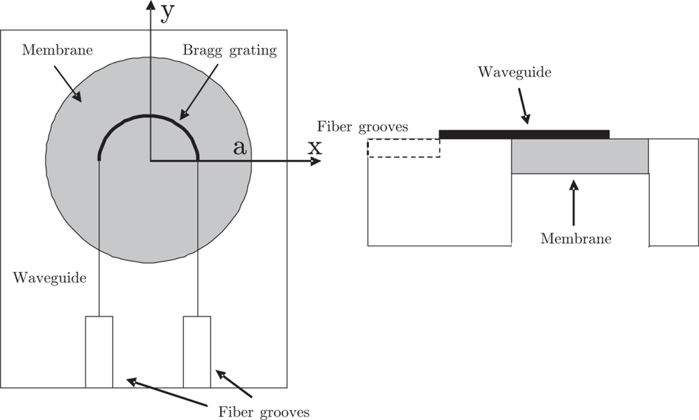
A very simple way to convert an applied pressure to a strain in the Bragg grating is to place the grating on a circular membrane. It is, however, important that the strain is uniform and longitudinal in order to increase the grating reflectivity and reduce the reflection peak bandwidth. Since the radial strain of a circular membrane is not constant, it is not practical to let the grating cross the membrane in a straight line, e.g., along a diameter. However, if the grating is placed in a waveguide following a circular curve at constant radial distance from the center of the membrane, the tangential strain at the waveguide position is constant along the length of the curve and linearly dependent on pressure and can thus be used for pressure sensing. An illustration of the device is shown in Figure 1. The effective index modulation necessary for Bragg reflection to occur can be obtained by modulating the waveguide height and/or width or by modulation of material properties. From a fabrication point of view, however, high corrugation depth combined with nanometer scale grating period and micrometer scale waveguide dimensions presents a challenge during definition of the sensor structure since high aspect ratios will occur. To avoid this problem the corrugations for this sensor are fabricated in both sides of the waveguide. Since the effective index of the waveguide is larger at the outer rim than at the inner rim, this design will effectively chirp the grating.
For isotropic plate materials the plate deflection w can be calculated from the well known Euler–Bernoulli equation
For a circular anisotropic, crystalline silicon plate of radius a Equation (4) is easily solved, and interestingly, the deflection shape for this specific case is identical to that of a circular isotropic plate
In fabricated devices thin dielectric films are deposited on the membrane, these will increase the effective flexural rigidity of the membrane due to the added thickness and due to a possible built-in stress. A built-in stress leads to additional terms on the left-hand side of Equation (4), where σαβ is the in-plane built-in stress, hf is the thickness of the thin film, while xα and xβ are the in-plane coordinates, i.e., x1 = x, and x2 = y [9]; in the case of an isotropic built-in stress σ0 the additional term is simply −hfσ0∇2w. From a simple minimum energy calculation using the unperturbed deflection shape, Equation (5), the effect of built-in stress may be corrected for by using a revised effective flexural rigidity Deff = [3 + k2 + 3k4 + hfσ0a2/ (2DH)] DH/8.
It is further noted that the sensor allows for an additional Bragg grating outside the plate, so that any wavelength shift not induced by pressure, e.g., temperature, may be compensated for by performing a differential measurement.
The design was also analyzed using the commercial finite element modeling (FEM) software Comsol. Taking advantage of the radial symmetry of the device, the FEM analysis can be reduced to a two dimensional anisotropic continuum analysis. Each layer was defined according to dimensions obtained during fabrication and using the materials library available in Comsol. Any measured intrinsic stress was also included in the model. Fixed boundary conditions are applied on the outer perimeter and a uniform pressure load on the upper surface. Using a triangular mesh of 25600 elements a convergent solution was found.
3. Fabrication
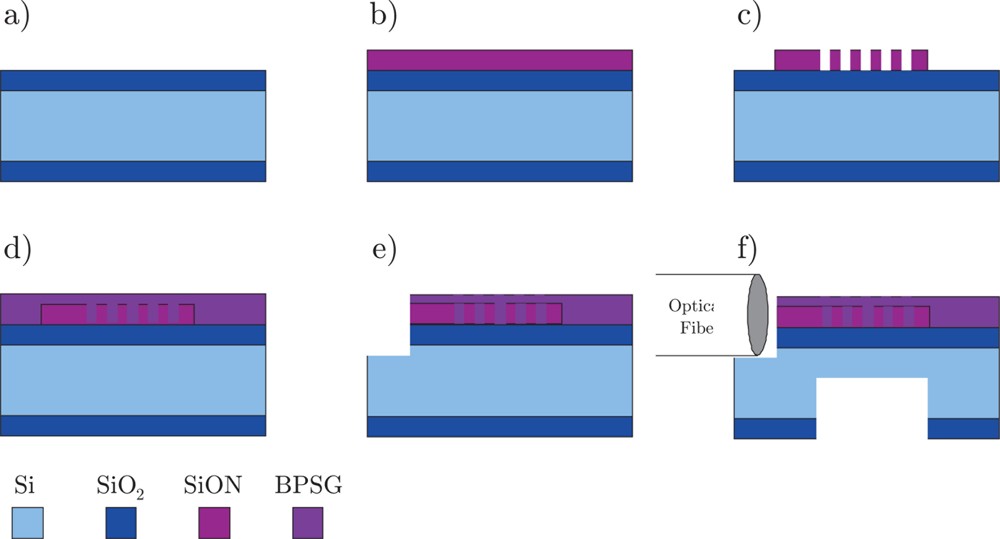
The sensor has been fabricated according to the process flow shown in Figure 2. An atmospheric pressure oxide (APOX) silicon wafer with approximately 8 μm of SiO2 on both sides is etched for 5 min in bHF (buffered hydrofluoric acid) in order to reduce surface roughness and remove any particles (a). The remaining SiO2 is acting as the lower cladding layer of the waveguide. The core of the waveguide is made from 2.5 μm SiON deposited by PECVD (b). The index contrast is approximately 0.02 and the core thickness allows for single mode waveguide operation at 1,550 nm wavelength. The Bragg grating is formed in the SiON by e-beam lithography (EBL) using the positive resist ZEP520a and a lift-off of 60 nm aluminum that is used as an etch mask in the following deep reactive ion etch (DRIE) (c). The upper cladding is made of borophosphosilicate glass (BPSG) that allows for re-flow during the following 1,000 °C anneal and thereby improved step coverage of the Bragg grating; the step coverage is in general otherwise insufficient in PECVD processes (d). The fiber grooves (e) and the membrane are both made by conventional UV lithography followed by an advanced oxide etch (AOE) and a DRIE silicon etch. The resulting membranes are 135 μm thick of which 112 μm is silicon and 23 μm is cladding layers (SiO2, SiON and BPSG).
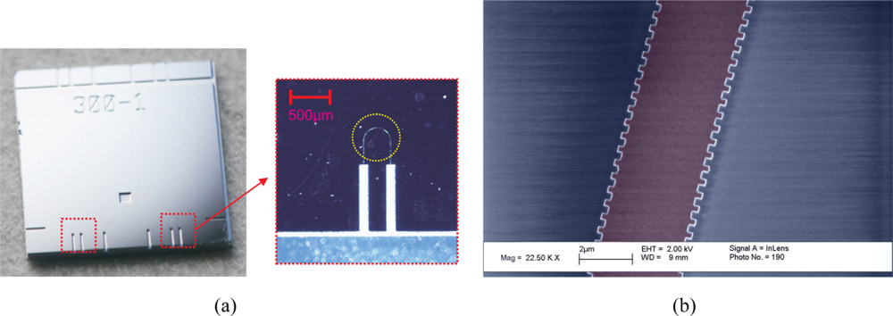
The final test chip is shown in Figure 3(a). The test chip is relatively large, 1 × 1 cm2, in order to facilitate and ease handling during characterization and contains two sensors as well as additional fiber grooves. The sensors each takes up an area of 1 × 1.8 mm2 and have membrane radii of 400 μm. A SEM image of the part of the waveguide containing the grating region is shown in Figure 3(b) at step (c) in the fabrication process. The corrugations in the sides of the waveguide are clearly seen and each have a width of 260 nm (Λ = 520 nm). In order to obtain a detectable reflection peak even for short gratings, the index modulation and thus the corrugation depth has to be sufficiently large. In this case a corrugation depth of 260 nm is used.
4. Results
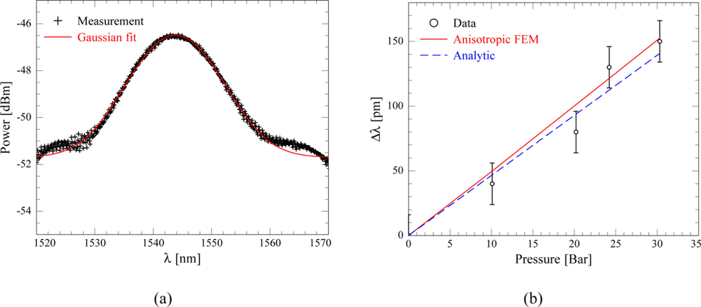
For characterization of the pressure sensitivity gas pressure was applied to the Bragg grating side of the membrane using a Druck DPI520 pressure controller and light was coupled to the test chip from a Koheras SuperK supercontinuum laser through a SMF-28 optical fiber. The reflected light was measured by means of a fiber optic circulator and an Agilent AQ-6315A optical spectrum analyzer. The spectrum of the reflected signal is seen in Figure 4(a), and from a Gaussian fit the center wavelength was found to be λB = 1543.8 nm, while the standard deviation is 16 pm and the full width half maximum of the peak is FWHM = 17.6 nm. This relatively large peak width is a result of the chirping mentioned in the design section. The Gaussian fit is applied using the linear power scale and a power offset is included. While other fitting functions could be used, the Gaussian fit agrees well with measured data.
The change in Bragg wavelength as a function of applied pressure for a 400 μm radius membrane sensor is plotted in Figure 4(b). A conservative estimate of the maximum allowable pressure, pmax, is found theoretically using a silicon yield strength of ≈ 1/10 the actual silicon yield strength [10], yielding pmax = 350 bar (350 ×105 Pa). Measurement uncertainties are primarily related to the quality of the Gaussian fit and to the accuracy of the pressure read-out from the pressure controller. A linear fit of the measurement data results in a slope of 4.8 pm/bar (4.8 ×10⁻⁵ pm/Pa). Considering the standard deviation of the Gaussian fit is 16 pm (shown as error bars in the plot), the measurements are easily within two standard deviations of the finite element method (FEM) model (full line) and the analytical results (dashed curve) as obtained from Equation (9). The lower Young’s modulus of the cladding layers have been included in the analytical calculation by using a thickness weighted average. This reduces the effective Young’s modulus to approximately 141 MPa.
Conventional electrical MEMS pressure sensors are typically based on either piezoresistive or capacitive technology [11,12]. It is common to implement these technologies using the deflection of a membrane or plate, equivalent to the optical sensor presented here. The sensitivity of the three technologies can thus be compared by simply considering the relative change in the measured quantity, approximately given as
The stress of the waveguide thin film was calculated from the measured change in wafer bow using Stoney’s equation [14], and an effective intrinsic stress of σ0 = −3.2 MPa was found; this value is so low that is does not affect the sensor sensitivity.
The coupling loss was measured to approximately 6 dB per coupling interface, which should be compared to the coupling loss of 4 dB calculated from the mode overlap integral for the fiber waveguide interface. The discrepancy may be attributed to alignment error. The transmission loss for the waveguides was measured to less than 1 dB/cm at 1,550 nm wavelength. The wavelength shift due to temperature change of the integrated Bragg grating is found by heating a test chip using a Peltier element. A temperature sensitivity of approximately 30 pm/K was found. The temperature sensitivity is primarily due to a large thermooptic coefficient of the waveguide material [15] and is comparable to the temperature sensitivities found in FBG sensors.
5. Conclusions
In this paper the design, fabrication and characterization of a new all-optical frequency modulated high pressure sensor has been presented. The sensor is well suited for distributed and remote sensing in harsh environments. The sensor is made with conventional MEMS materials and technology combined with e-beam lithography for nanostructuring of the Bragg grating, which allows for simple fabrication and high mechanical stability. The pressure sensitivity of the sensor was measured to be 4.8 pm/bar (4.8 × 10⁻⁵ pm/Pa) and the temperature sensitivity was measured to be 30 pm/K. The design could be optimized for higher or lower sensitivities by adjusting the membrane dimensions.
Acknowledgments
Center for Individual Nanoparticle Functionality (CINF) is sponsored by The Danish National Research Foundation.
References
- Fu, H.; Fu, J.; Qiao, X. High sensitivity fiber Bragg grating pressure difference sensor. Chinese Optics Lett 2004, 2, 621–623. [Google Scholar]
- Wang, X.; Li, B.; Xiao, Z.; Lee, S.H.; Roman, H.; Russo, O.L.; Chin, K.K.; Farmer, K.R. An ultra-sensitive optical MEMS sensor for partial discharge detection. J. Micromech. Microeng 2005, 15, 521–527. [Google Scholar]
- Wagner, D.; Frankenberger, J.; Deimel, P.P. Optical pressure sensor using two Mach-Zehnder interferometers for the TE and TM polarization. J. Micromech. Microeng 1994, 4, 35–39. [Google Scholar]
- Liu, L.; Zhang, H.; Zhao, Q.; Liu, Y.; Li, F. Temperature-independent FBG pressure sensor with high sensitivity. Opt. Fiber Techn 2007, 13, 78–80. [Google Scholar]
- Graham-Rowe, D. Sensors take the strain. Nature Photon 2007, 1, 307–309. [Google Scholar]
- Fragiacomo, G.; Reck, K.; Lorenzen, L.; Thomsen, E.V. Novel designs for application specific MEMS pressure sensors. Sensors 2010, 10, 9541–9563. [Google Scholar]
- Holgate, C. The transverse flexure of perforated aeolotropic plates. Proc. Roy. Soc. A Mathe. Phys. Eng. Sci 1946, 185, 50–69. [Google Scholar]
- Boresi, A.P; Sidebottom, O.M. Advanced Mechanics of Materials; John Wiley & Sons: New York, NY, USA, 1985; pp. 474–479. [Google Scholar]
- Landau, L.D.; Lifshitz, E.M. Theory of Elasticity; Butterworth-Heinemann: Oxford, UK, 1986; pp. 50–53. [Google Scholar]
- Petersen, K.E. Silicon as a mechanical material. Proc. IEEE 1982, 70, 420–457. [Google Scholar]
- Lin, L.; Yun, W. Design, optimization and fabrication of surface micromachined pressure sensors. Mechatronics 1998, 8, 505–519. [Google Scholar]
- Pedersen, T.; Fragiacomo, G.; Hansen, O.; Thomsen, E.V. Highly sensitive micromachined capacitive pressure sensor with reduced hysteresis and low parasitic capacitance. Sens. Actuat. A Phys 2009, 154, 35–41. [Google Scholar]
- Barlian, A.A.; Park, W.-T.; Mallon, J.R.; Rastegar, A.J.; Pruitt, B.L. Review: Semiconductor piezoresistance for microsystems. Proc. IEEE 2009, 97, 513–552. [Google Scholar]
- Stoney, G.G. The tension of metallic films deposited by electrolysis. Proc. Roy. Soc. Lond 1909, 82, 172–175. [Google Scholar]
- Eldada, L. Polymer integrated optics: Promise vs. practicality. Organic Photon. Mater. Dev. IV 2002, 4642, 11–22. [Google Scholar]
© 2011 by the authors; licensee MDPI, Basel, Switzerland. This article is an open access article distributed under the terms and conditions of the Creative Commons Attribution license (http://creativecommons.org/licenses/by/3.0/).
Share and Cite
Reck, K.; Thomsen, E.V.; Hansen, O. All-Optical Frequency Modulated High Pressure MEMS Sensor for Remote and Distributed Sensing. Sensors 2011, 11, 10615-10623. https://doi.org/10.3390/s111110615
Reck K, Thomsen EV, Hansen O. All-Optical Frequency Modulated High Pressure MEMS Sensor for Remote and Distributed Sensing. Sensors. 2011; 11(11):10615-10623. https://doi.org/10.3390/s111110615
Chicago/Turabian StyleReck, Kasper, Erik V. Thomsen, and Ole Hansen. 2011. "All-Optical Frequency Modulated High Pressure MEMS Sensor for Remote and Distributed Sensing" Sensors 11, no. 11: 10615-10623. https://doi.org/10.3390/s111110615
APA StyleReck, K., Thomsen, E. V., & Hansen, O. (2011). All-Optical Frequency Modulated High Pressure MEMS Sensor for Remote and Distributed Sensing. Sensors, 11(11), 10615-10623. https://doi.org/10.3390/s111110615