1. Introduction
Complementary metal-oxide-semiconductor (CMOS) image sensors offer many advantages over CCDs’, such as system-on-chip, low power consumption and possibly lower cost of camera systems [
1,
2]. The pinned photodiode technology introduced to CMOS image sensors in mid-90s effectively reduces the dark current and cancels the
kTC noise of pixels, and attains high conversion gain [
3]. As a result, the noise level of recent CMOS image sensors is becoming even better than CCD image sensors, especially for applications that high frame-rate is required. Low-noise high-gain column readout circuits used for pixel noise cancelling and signal sampling are greatly contributing to the reduction of the readout random noise [
4–
7]. This high-gain column amplifier reduces the noise of wideband amplifiers at the output of image sensors by a factor of the gain, and if the amplifier reset noise is cancelled, the thermal noise due to the pixel source follow (SF) amplifier can be reduced by a factor of square root of the gain [
7]. Nevertheless, for next-generation low-noise CMOS image sensors, advanced noise reduction techniques are needed in order to more effectively reduce the pixel SF amplifier noises, especially 1/
f and random telegraph signal (RTS) noises and maintain the signal dynamic range.
In this paper, the noise reduction effects of another type of column-parallel high-gain signal readout circuits, correlated multiple sampling (CMS) circuits, for CMOS image sensors are discussed. In the CMS, both reset and signal levels of pixel outputs are sampled for multiple times and summed up, and the difference of the average of the two levels is calculated for pixel-related noise cancelling. Two types of the CMS circuits are proposed. One is with a simple integration and the other is with a folding integration. In the folding integrator, the signal swing of the integrator output is suppressed by a negative feedback using a comparator (one-bit analog-to-digital converter (ADC)) and a one-bit digital-to-analog converter (DAC). This allows us to reduce the readout noise while maintaining the signal dynamic range. A prototype 1Mpixel CMOS image sensor with pinned photodiodes and the column-parallel CMS circuits has been implemented. The noise measurement results show an interesting behavior for low-noise pixels and noisy pixels. The noise behavior in low-noise pixels due to thermal and 1/f noises and noisy pixels due to RTS and RTS-like noises is discussed with a noise analysis using a transfer function of the CMS.
3. Noise Reduction Effects of Correlated Multiple Sampling Circuits
The noise reduction effect of the CMS circuits for thermal, 1/
f and RTS noises can be calculated in frequency domain if the noise power spectrum and transfer function of the CMS operation are known. The transfer function of the CMS circuits as a discrete time system can be obtained from
Equation (5). The interval of the two multiple samples
Tg influences to the 1/
f noise reduction effect. For simplicity,
Tg is supposed to be integer multiple of the sampling time
T0. Therefore,
Tg is given by
MgT0, where
Mg is an integer. The final output of the CMS circuits as a function of discrete time, Δ
VSC(
nT0) is written as
where
T0 is the sampling period,
VP ((
n −
k)
T0) and
VP ((
n −
k −
M −
Mg + 1)
T0) are reset and signal levels of pixel outputs of the
k-th sample, respectively. The transfer function of the CMS is obtained with
z-transform, and is expressed in the
z domain as
If
Mg = 1, then it is simplified to
The output noise power,
after the CMS process is calculated as
where
Sn (
f) is a noise spectrum of the pixel source follower and
ωc is the cut-off angular frequency of the sampling circuits in the CMS. The noise power spectrum of the pixel source follower is given by
where
Snt is the power spectrum density of the thermal noise,
kf is the flicker noise coefficient, and
kRTS and
τRTS are the RTS noise coefficient and relaxation time, respectively, of the RTS noise. The RTS noise due to a single trap has a Lorentzian-type spectrum as given by the third term of
Equation (15), and
τRTS is given by
where
τc and
τe are mean time that the trap in the gate oxide captures and emits an electron, respectively [
7].
The thermal noise with the CMS operation can be calculated without performing the integration of
Equation (14) as
if
ωCMS ≪
ωc, where
ωCMS is the bandwidth (
cuf-off angular frequency) of the CMS circuits given by
Therefore the thermal noise power is reduced in inverse proportion to M as shown in
Figure 6 due to bandwidth limitation effect.
From
Equation (12) with
z = exp(
jωT0), the noise power transfer function for the CMS is given by
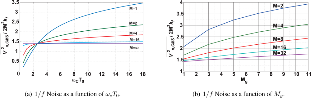
The 1/
f noise power with the CMS operation can be calculated by
Equation (14) and
(19). The result as a function of
ωcT0 is shown in
Figure 7(a) for
Mg = 1 [
10]. The noise power is normalized with 2
M2kf. In the case of M = 1, the CMS is operating as the correlatd double sampling (CDS) [
9]. For M = ∞, it approaches 1.39 which corresponds to a differential averager using continuous integration [
7]. The noise power as a function of
Mg is shown in
Figure 7(b). The noise power has a tendency to increase as
Mg increases. For effective noise reduction,
Mg should be minimized.
From
Equation (14) and the third term of
Equation (15), the normalized noise power with
kRTS is given by
where
ωRTS = 1/
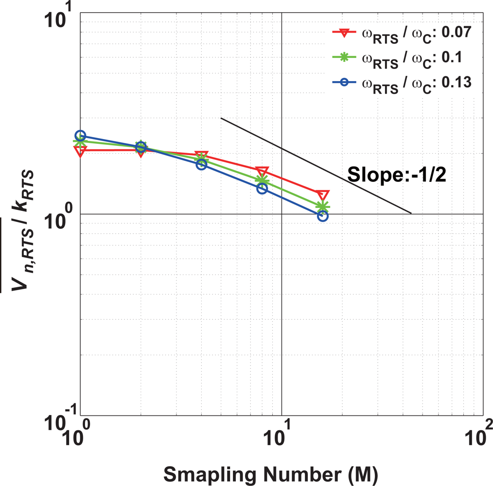
τRTS. The calculated RTS noise after the CMS process is shown in
Figure 8. It shows the noise amplitude normalized by
kRTS as a function of the number of samplings. Three curves for
ωRTS/
ωC = 0.07, 0.1 and 0.13 are plotted. If the bandwidth of the CMS,
ωCMS determined by M is smaller than
ωRTS, the noise reduction effect becomes efficient and the gradient of the noise amplitude to M approaches −1/2.
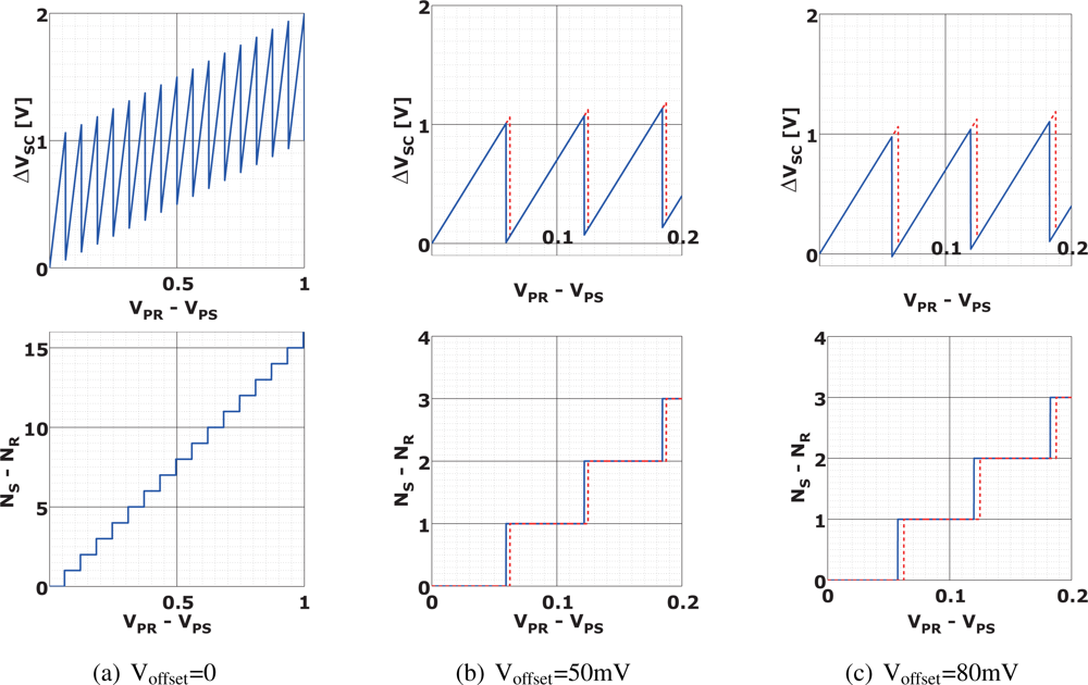
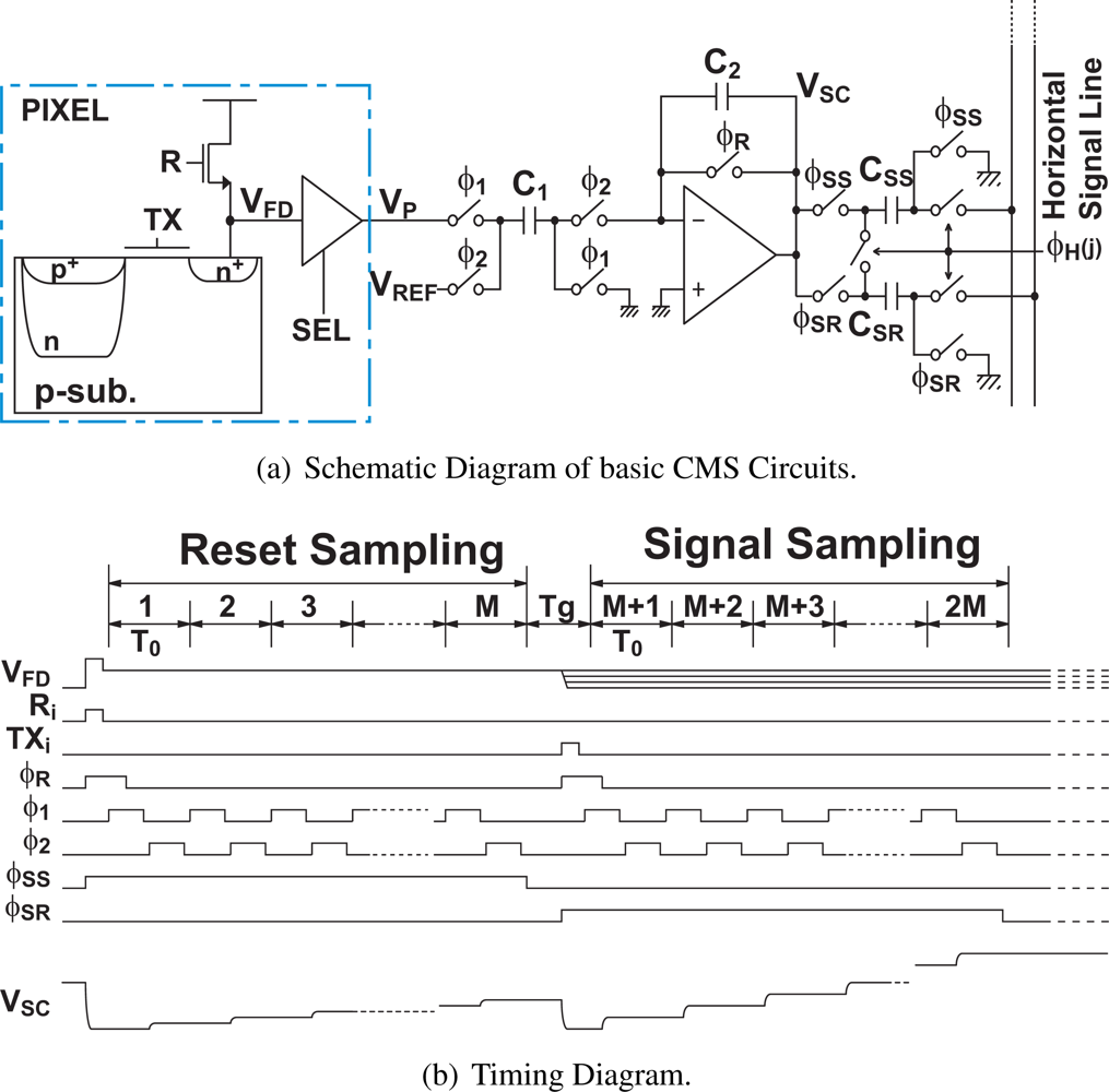
4. Measurement Results
A 1Mpixel CMOS image sensor with column-parallel FI-CMS circuits for the low-noise wide dynamic range readout is implemented with 0.18
μm CMOS technology with pinned photodiodes. The chip photomicrograph is shown in
Figure 9. In this chip, the operation of the SI-CMS is also possible by disabling the function of folding. The pixel type is a 4-Tr pinned photodiode active pixel. The specifications of the CMOS image sensor are summarized in
Table 1. The number of effective pixels is 1,024(H) × 1,024(V), the pixel size is 7.5
μm × 7.5
μm, and the conversion gain is 35
μV/
e−. Chip outputs are come out by 4 channel output buffers, and are comprised of analog residue signals and counter output codes.
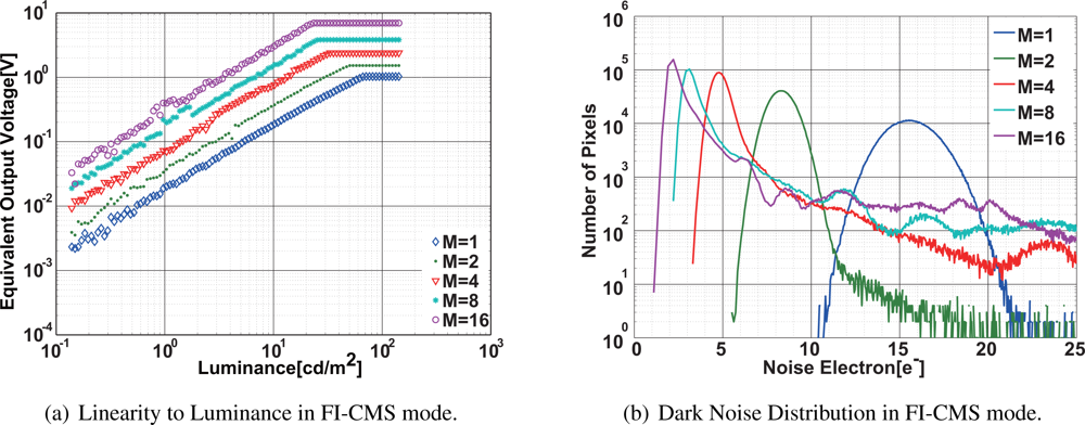
Figure 10(a) shows measurement results of the linearity of the implemented CMOS image sensor operating in the SI-CMS mode. Though the linearity is degraded at large output swing for M = 1, the gain of the signal in the linear region almost exactly follows the number of samplings. The dark noise distribution of the 1Mpixel CMOS image sensor is shown in
Figure 10(b). The noise electron at the peak of distribution is about 15.6
e− when the sampling number is 1. The noise electron is reduced to smaller than 2
e− for the sampling number of 16. The noise distribution is entirely shifted to the lower noise as increasing the number of samplings.
Using the noise distribution shown in
Figure 10(b), a cumulative probability (C.P.)
P(
y) of the temporal noise as a function of noise electrons given by
is calculated as shown in
Figure 11, where
h(
x) is the distribution as a function of the noise electrons (
x). The pixel noise sources are mainly thermal and 1/
f noises of the source follower amplifier. However, some pixels have a large noise due to RTS and RTS-like noises. The tailing part of distribution of the cumulative probability (< 10
−4) is due to the RTS- and RTS-like noise. Therefore, pixels are roughly classified into two types, low noise (C.P. > 10
−4), and noisy pixels (C.P. < 10
−4). In low noise region, the dominant noise components are the thermal and 1/
f noises. In large noise region, the noisy pixels are mainly due to RTS or RTS-like noises [
11]. The results of
Figure 11 show that the CMS has a noise reduction effect of RTS and RTS-like noises if the number of samplings is increased.
Figure 12 shows behaviors of the low-noise and noisy pixels when the number of samplings is increased. Two plots show the values of noise electrons for low-noise and noisy pixels at 90 and 0.01% of cumulative probabilities, respectively. In the low-noise pixels, the noise amplitude is in inverse proportion to M, for
M ≤ 4. This means that the dominant noise comes from the circuits and systems connected at the back of the CMS integrator such as output buffers and external ADCs. For M > 4, the CMS has a tendency of noise reduction in inverse proportion to square root of M. In this region, the dominant noise is due to thermal noise of the pixel source follower as predicted by
Equations (17) and
(18). Though it is not clearly shown in
Figure 12, the noise reduction effect of the CMS is limited by the 1/
f noise of the pixel source follower if the number of samplings is increased to larger than 16 as predicted by results of
Figure 7(a). In the noisy pixels, the noise reduction effect of the CMS is very small for M ≤ 4, and the noise reduction factor (
) seems to approach to −1/2 for M > 4. This result could be explained by the results of
Figure 8 if the dominant noise is the RTS noise and 0.001% of the pixels (noisy pixels) takes
ωRTS/ωC of around 0.1. However, further detailed measurements and analysis are necessary to conclude it.
Figure 13(a) and
13(b) show characteristics of the linearity and the dark noise distribution with the 1Mpixel CMOS image sensor using the column-parallel FI-CMS, respectively. In the linearity, the equivalent output signal
is calculated in digital domain using the value of (
NS −
NR), and Δ
VSC of
Equation (10). The gain of the signal in the linear region follows the number of samplings. An important difference compared with the linear measurement results of SI-CMS (
Figure 10(a)) is that the equivalent output is not limited to the maximum output swing of the integrator even though the number of samplings is increased to 16 while the output of the SI-CMS is limited to the maximum output swing of about 1 V. The maximum equivalent output swing of the FI-CMS is 6.94 V using M = 16 and the power supply voltage of 3.3 V. This shows the effectiveness for the wide dynamic range of the FI-CMS.
The problem of the FI-CMS of the present design when compared with that of the SI-CMS is the degradation of linearity and longer tailing of the dark noise distribution, as shown in
Figure 13. A possible reason of the degradation is a coupling of digital signal lines running along sensitive analog circuit nodes in the column. In the SI-CMS mode, these digital lines are always fixed to “0”. As shown in the noise distribution of
Figure 13(b), the FI-CMS has a noise reduction effect of the multiple sampling similar to that of the SI-CMS. Theoretically, the FI-CMS has the same noise reduction effect as that of the SI-CMS. Since the pixel outputs have large offset deviations, the influence of the coupling noise depends on the pixel source follower offsets. In most of the pixels, the influence of the digital signal coupling noise is cancelled out by the CDS operation if the reset and signal samplings have the same operation. However, in some pixels, the CDS does not completely cancel the coupling noise due to the FI-CMS operation, and population of noisy pixel increases. Therefore, the tailing of the distribution in
Figure 13(b) is due to large digital signal coupling noises. The majority of the noise distribution around the peak has a behavior similar to that of the SI-CMS. The mean value of the distribution is 2.2 electrons, which corresponds to the input-referred noise of 77
μVrms.
Table 2 shows a summary of measurement results of noise and dynamic range. In the case of the simple integration, the noise is reduced to smaller than 2 electrons while sacrificing the dynamic range to be 59.4 dB. On the other hand, in the case of the folding integration, the dynamic range of 75.0 dB (= 6.94
V/ (16 × 77
μV)) is attained while reducing the noise to 2.2 electrons.


