
Photoelectric Performance of Two-Dimensional n-MoS2 Nanosheets/p-Heavily Boron-Doped Diamond Heterojunction at High Temperature


Abstract
1. Introduction
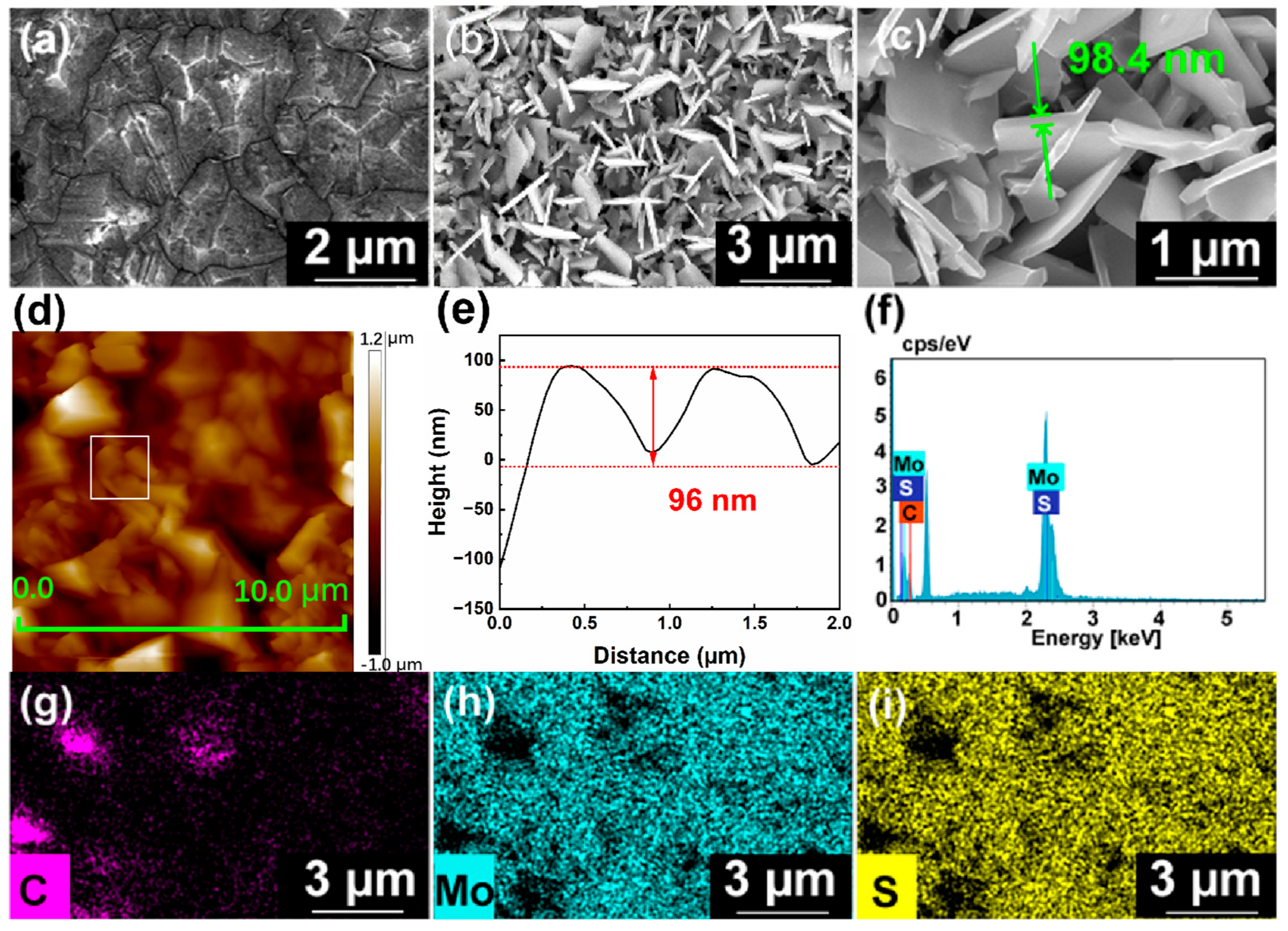
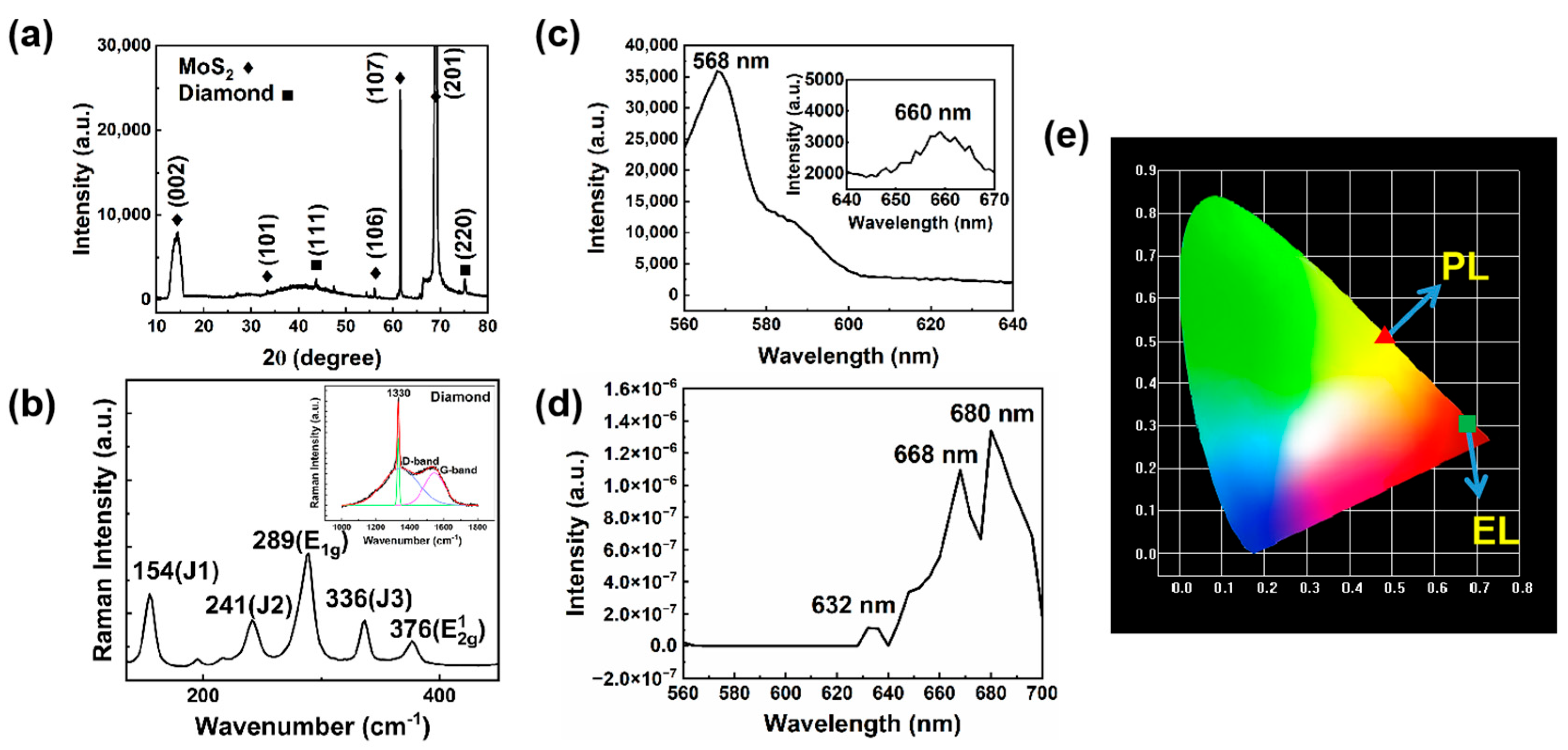
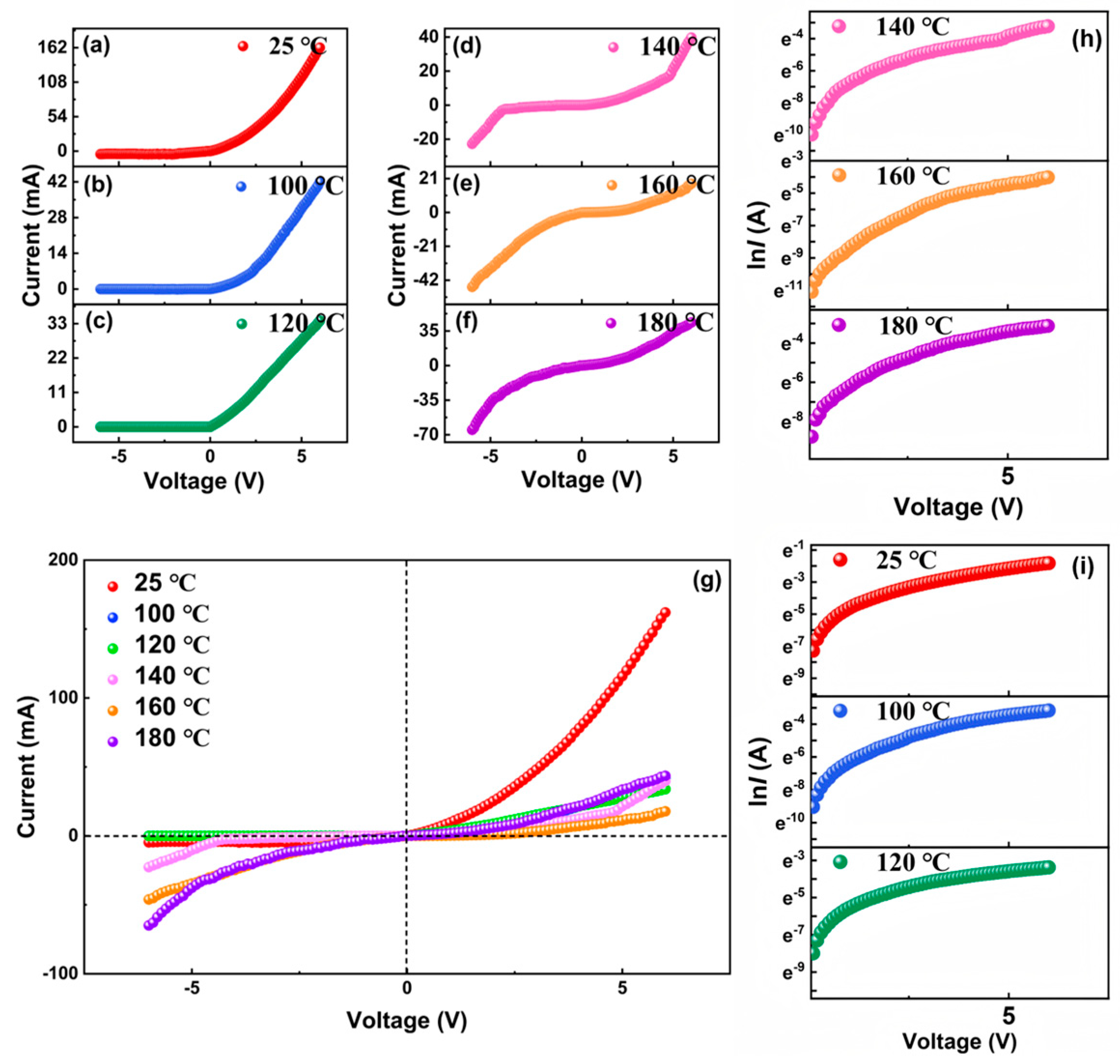
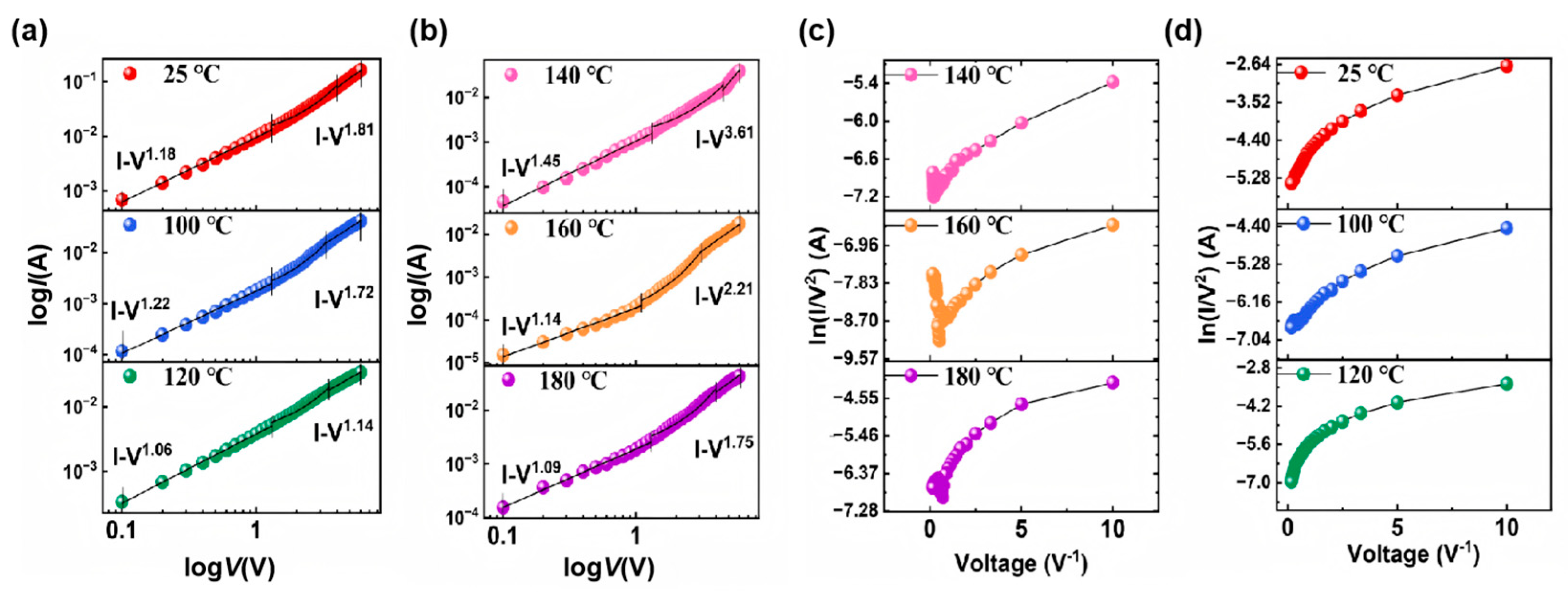
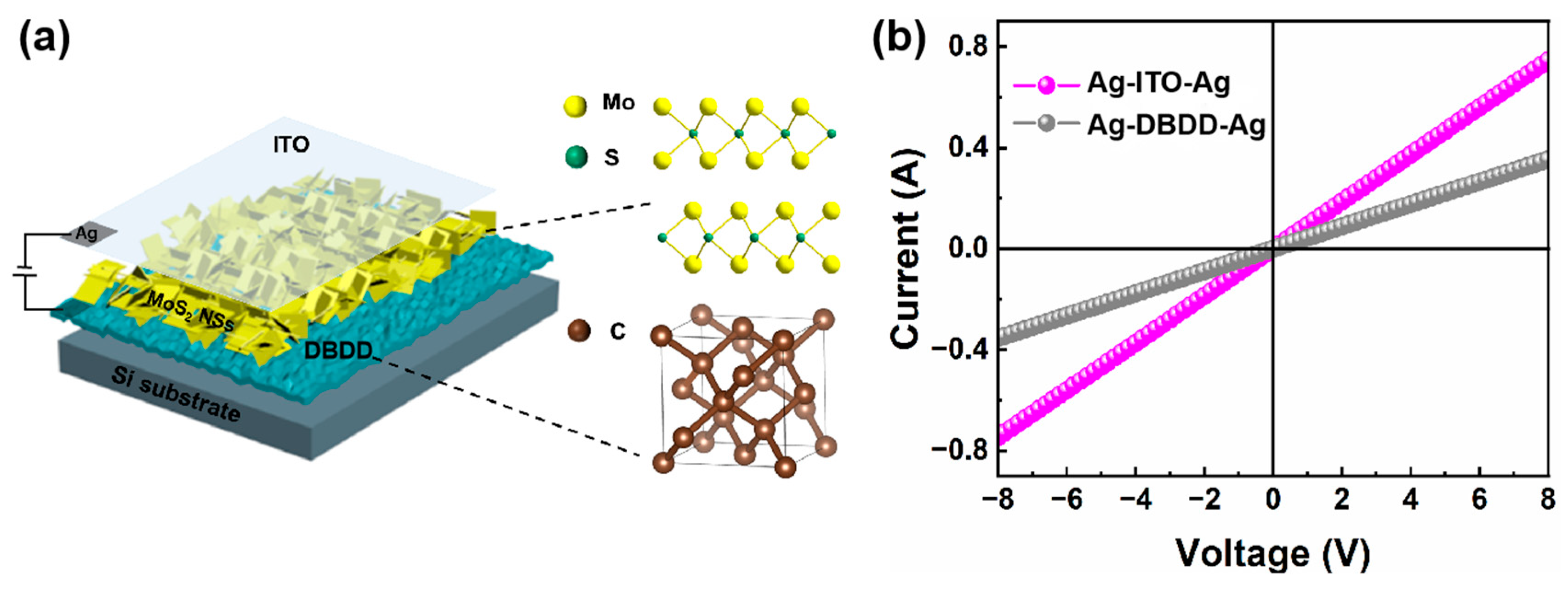
2. Results and Discussion
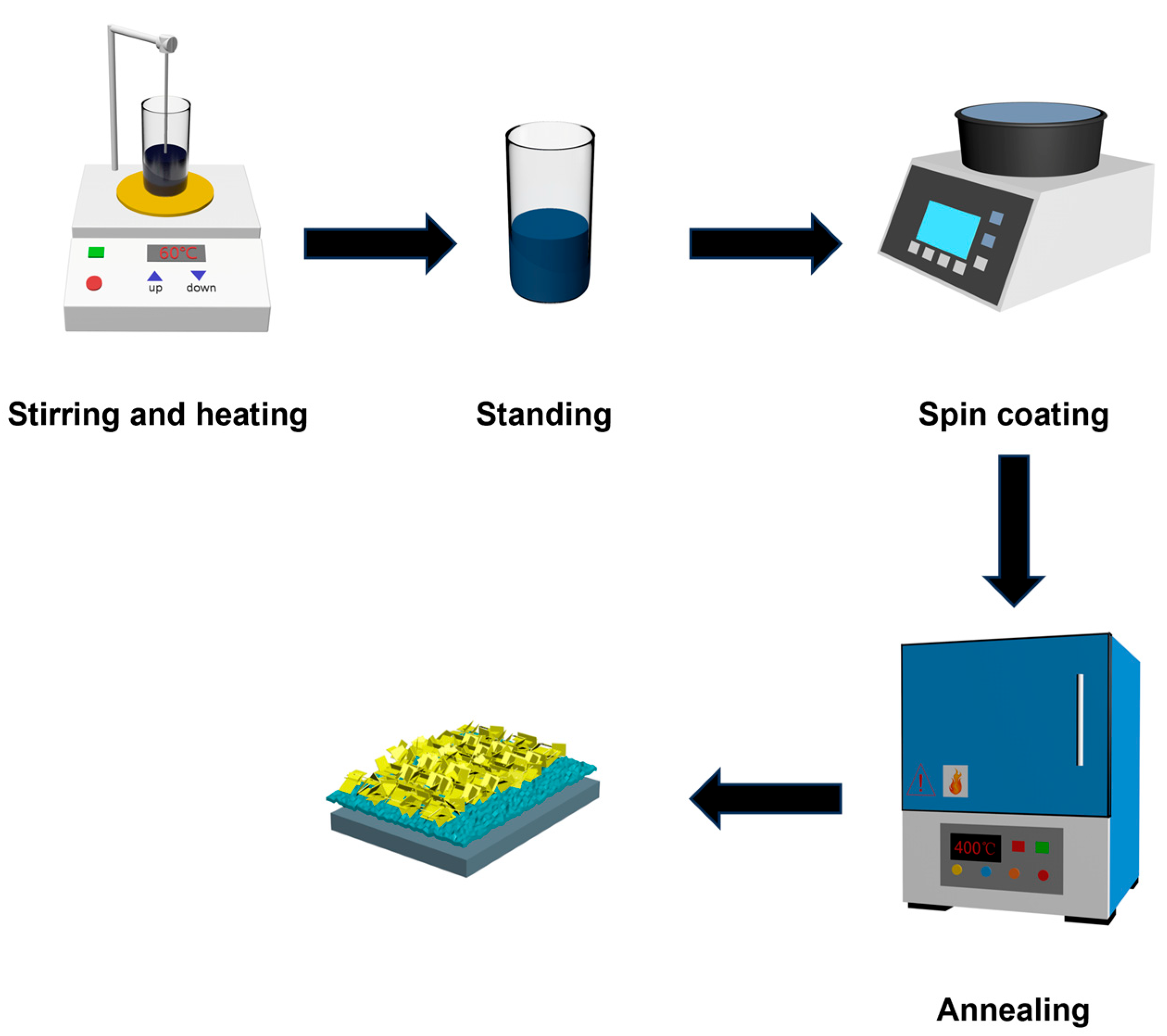
3. Materials and Methods
4. Conclusions
Author Contributions
Funding
Data Availability Statement
Conflicts of Interest
References
- Liu, L.W.; Liu, C.S.; Huang, X.H.; Zeng, S.F.; Tang, Z.W.; Zhang, D.W.; Zhou, P. Tunable Current Regulative Diode Based on Van der Waals Stacked MoS2/WSe2 Heterojunction–Channel Field-Effect Transistor. Adv. Electron. Mater. 2022, 8, 2100869. [Google Scholar] [CrossRef]
- Nalwa, H.S. A review of molybdenum disulfide (MoS2) based photodetectors: From ultra-broadband, self-powered to flexible devices. RSC Adv. 2020, 10, 30529–30602. [Google Scholar] [CrossRef]
- Zou, L.R.; Sang, D.D.; Yao, Y.; Wang, X.T.; Zheng, Y.Y.; Wang, N.Z.; Wang, C.; Wang, Q.L. Research progress of optoelectronic devices based on two-dimensional MoS2 materials. Rare Met. 2023, 42, 17–38. [Google Scholar] [CrossRef]
- Zou, L.R.; Lyu, X.D.; Sang, D.D.; Yao, Y.; Ge, S.H.; Wang, X.T.; Zhou, C.D.; Fu, H.L.; Xi, H.Z.; Fan, J.C.; et al. Two-dimensional MoS2/diamond based heterojunctions for excellent optoelectronic devices: Current situation and new perspectives. Rare Met. 2023, 42, 3201–3211. [Google Scholar] [CrossRef]
- Wu, F.; Tian, H.; Shen, Y.; Hou, Z.; Ren, J.; Gou, G.; Sun, Y.; Yang, Y.; Ren, T.L. Vertical MoS2 transistors with sub-1-nm gate lengths. Nature 2022, 603, 259–264. [Google Scholar] [CrossRef]
- Evans, J.M.; Lee, K.S.; Yan, E.X.; Thompson, A.C.; Morla, M.B.; Meier, M.C.; Ifkovits, Z.P.; Carim, A.I.; Lewis, N.S. Demonstration of a Sensitive and Stable Chemical Gas Sensor Based on Covalently Functionalized MoS2. ACS Mater. Lett. 2022, 4, 1475–1480. [Google Scholar] [CrossRef]
- Liu, C.; Lu, Y.; Yu, X.; Shen, R.; Wu, Z.; Yang, Z.; Yan, Y.; Feng, L.; Lin, S. Hot carriers assisted mixed-dimensional graphene/MoS2/p-GaN light emitting diode. Carbon 2022, 197, 192–199. [Google Scholar] [CrossRef]
- Liu, X.; Hu, S.; Lin, Z.; Li, X.; Song, L.; Yu, W.; Wang, Q.; He, W. High-performance MoS2 photodetectors prepared using a patterned gallium nitride substrate. ACS Appl. Mater. Interfaces 2021, 13, 15820–15826. [Google Scholar] [CrossRef]
- Yang, S.; Liu, Y.; Wu, Y.; Guo, F.; Zhang, M.; Zhu, X.; Xua, R.; Hao, L. High-performance flexible photodetectors based on CdTe/MoS2 heterojunction. Nanoscale 2024, 16, 13932–13937. [Google Scholar] [CrossRef]
- Samy, O.; Zeng, S.; Birowosuto, M.D.; El Moutaouakil, A. A review on MoS2 properties, synthesis, sensing applications and challenges. Crystals 2021, 11, 355. [Google Scholar] [CrossRef]
- Jeong, Y.; Lee, H.J.; Park, J.; Lee, S.; Jin, H.J.; Park, S.; Cho, H.; Hong, S.; Kim, T.; Kim, K.; et al. Engineering MoSe2/MoS2 heterojunction traps in 2D transistors for multilevel memory, multiscale display, and synaptic functions. Npj 2D Mater. Appl. 2022, 6, 23. [Google Scholar] [CrossRef]
- Jeong, M.H.; Ra, H.S.; Lee, S.H.; Kwak, D.H.; Ahn, J.; Yun, W.S.; Lee, J.; Chae, W.S.; Hwang, D.K.; Lee, J.S. Multilayer WSe2/MoS2 Heterojunction Phototransistors through Periodically Arrayed Nanopore Structures for Bandgap Engineering. Adv. Mater. 2022, 34, 2108412. [Google Scholar] [CrossRef] [PubMed]
- Xiang, X.; Qiu, Z.; Zhang, Y.; Chen, X.; Wu, Z.; Zheng, H.; Zhang, Y. Gain-type photodetector with GFET-coupled MoS2/WSe2 heterojunction. J. Alloys Compd. 2024, 1002, 175475. [Google Scholar] [CrossRef]
- Jian, P.; Cai, X.; Zhao, Y.; Li, D.; Zhang, Z.; Liu, W.; Xu, D.; Liang, W.; Zhou, X.; Dai, J.; et al. Large-scale synthesis and exciton dynamics of monolayer MoS2 ondifferently doped GaN substrates. Nanophotonics 2023, 12, 4475–4484. [Google Scholar] [CrossRef]
- Wang, W.; Wang, W.; Meng, Y.; Quan, Q.; Lai, Z.; Li, D.; Xie, P.; Yip, S.; Kang, X.; Bu, X.; et al. Mixed-Dimensional Anti-ambipolar Phototransistors Based on 1D GaAsSb/2D MoS2 Heterojunctions. ACS Nano 2022, 16, 11036–11048. [Google Scholar] [CrossRef]
- Parveen, S.; Pal, P.K.; Mukhopadhyay, S.; Majumder, S.; Bisoi, S.; Rahman, A.; Barman, A. Hot carrier dynamics in the BA2PbBr4/MoS2 heterostructure. Nanoscale 2025, 17, 2800. [Google Scholar] [CrossRef]
- Nguyena, S.T.; Pham, K.D. Theoretical prediction of the electronic structure, optical properties and contact characteristics of a type-I MoS2/MoGe2N4 heterostructure towards optoelectronic devices. Dalton Trans. 2024, 53, 9072–9080. [Google Scholar] [CrossRef]
- Yao, Y.; Sang, D.; Duan, S.; Wang, Q.; Liu, C. Review on the Properties of Boron-Doped Diamond and One-Dimensional-Metal-Oxide Based PN Heterojunction. Molecules 2020, 26, 71. [Google Scholar] [CrossRef]
- Wang, L.; Cheng, S.; Wu, C.; Pei, K.; Song, Y.; Li, H.; Wang, Q.; Sang, D. Fabrication and high temperature electronic behaviors of n-WO3 nanorods/p-diamond heterojunction. Appl. Phys. Lett. 2017, 110, 052106. [Google Scholar] [CrossRef]
- Wang, Q.; Yao, Y.; Sang, X.; Zou, L.; Ge, S.; Wang, X.; Zhang, D.; Wang, Q.; Zhou, H.; Fan, J.; et al. Photoluminescence and Electrical Properties of n-Ce-Doped ZnO Nanoleaf/p-Diamond Heterojunction. Nanomaterials 2022, 12, 3773. [Google Scholar] [CrossRef]
- Lin, W.; Wang, T.T.; Wang, Q.L.; Lv, X.Y.; Li, G.Z.; Li, L.A.; Zou, G.T. Design of vertical diamond Schottky barrier diode with junction terminal extension structure by using the n-Ga2O3/p-diamond heterojunction. Chin. Phys. B 2022, 31, 108105. [Google Scholar] [CrossRef]
- Yao, Y.; Sang, D.; Duan, S.; Wang, Q.; Liu, C. Excellent optoelectronic applications and electrical transport behavior of the n-WO3 nanostructures/p-diamond heterojunction: A new perspective. Nanotechnology 2021, 32, 332501. [Google Scholar] [CrossRef]
- Zou, L.; Sang, D.; Ge, S.; Yao, Y.; Wang, G.; Wang, X.; Fan, J.; Wang, Q. High-temperature optoelectronic transport behavior of n-MoS2 nanosheets/p-diamond heterojunction. J. Alloys Compd. 2024, 972, 172819. [Google Scholar] [CrossRef]
- Clavel, M.B.; Liu, J.-S.; Meeker, M.A.; Khodaparast, G.A.; Xie, Y.; Heremans, J.J.; Bhattacharya, S.; Hudait, M.K. Electronic and optical properties of highly boron-doped epitaxial Ge/AlAs(001) heterostructures. J. Appl. Phys. 2020, 127, 075702. [Google Scholar] [CrossRef]
- Sang, D.; Liu, J.; Wang, X.; Zhang, D.; Ke, F.; Hu, H.; Wang, W.; Zhang, B.; Li, H.; Liu, B.; et al. Negative differential resistance of n-ZnO nanorods/p-degenerated diamond heterojunction at high temperatures. Front. Chem. 2020, 8, 531. [Google Scholar] [CrossRef]
- Huang, J.; Meng, A.; Zhang, Z.; Ma, G.; Long, Y.; Li, X.; Xiang, B.; Han, P.; He, B. BiVO4/boron-doped diamond heterojunction photoanode with boron doping engineering and enhanced photoelectrocatalytic activity. Diam. Relat. Mater. 2023, 138, 110226. [Google Scholar] [CrossRef]
- Su, T.H.; Chiang, C.H.; Lin, Y.J. Temperature dependence of current–voltage characteristics of MoS2/Si devices prepared by the chemical vapor deposition method. Microelectron. Reliab. 2017, 78, 374–378. [Google Scholar] [CrossRef]
- Li, P.; Yuan, K.; Lin, D.Y.; Wang, T.; Du, W.; Wei, Z.; Watanabe, K. p-MoS2/n-InSe van der Waals heterojunctions and their applications in all-2D optoelectronic devices. RSC Adv. 2019, 9, 35039–35044. [Google Scholar] [CrossRef]
- Zhang, L.; Cheng, S.; Wang, L.; Pei, K.; Li, H. High temperature UV photodetectors based on the negative differential resistance effect of WO3/diamond PN junctions. Appl. Phys. Lett. 2023, 122, 182102. [Google Scholar] [CrossRef]
- Zhang, K.; Feng, S.; Kang, S.; Wu, Y.; Zhang, M.; Wang, Q.; Tao, Z.; Fan, Y.; Lu, W. Hybrid structure of PbS QDs and vertically-few-layer MoS2 nanosheets array for broadband photodetector. Nanotechnology 2021, 32, 145602. [Google Scholar] [CrossRef]
- Zhang, Y.; Zeng, W.; Li, Y. The hydrothermal synthesis of 3D hierarchical porous MoS2 microspheres assembled by nanosheets with excellent gas sensing properties. J. Alloys Compd. 2018, 749, 355–362. [Google Scholar] [CrossRef]
- He, H.Y.; He, Z.; Shen, Q. Efficient hydrogen evolution catalytic activity of graphene/metallic MoS2 nanosheet heterostructures synthesized by a one-step hydrothermal process. Int. J. Hydrogen Energy 2018, 43, 21835–21843. [Google Scholar] [CrossRef]
- Li, H.; Zhang, T.; Li, L.; Lu, X.; Li, B.; Jin, Z.; Zou, J. Investigation on crystalline structure, boron distribution, and residual stresses in freestanding boron-doped CVD diamond films. J. Cryst. Growth 2010, 312, 1986–1991. [Google Scholar] [CrossRef]
- Knight, D.S.; White, W.B. Characterization of diamond films by Raman spectroscopy. J. Mater. Res. 1989, 4, 385–393. [Google Scholar] [CrossRef]
- Kumar, D.; Chandran, M.; Rao, M.S.R. Effect of boron doping on first-order Raman scattering in superconducting boron doped diamond films. Appl. Phys. Lett. 2017, 110, 191602. [Google Scholar] [CrossRef]
- Ferrari, A.C.; Robertson, J. Interpretation of Raman spectra of disordered and amorphous carbon. Phys. Rev. B 2000, 61, 14095. [Google Scholar] [CrossRef]
- Huang, J.; Dong, Z.; Li, Y.; Li, J.; Tang, W.; Yang, H.; Wang, J.; Bao, Y.; Jin, J.; Li, R. MoS2 nanosheet functionalized with Cu nanoparticles and its application for glucose detection. Mater. Res. Bull. 2013, 48, 4544–4547. [Google Scholar] [CrossRef]
- Erkan, S.; Altuntepe, A.; Zan, R. Synthesis of MoS2 thin films using the two-step approach. Niğde Ömer Halisdemir Üniversitesi Mühendislik Bilim. Derg. 2023, 12, 297–301. [Google Scholar] [CrossRef]
- Liu, Z.; Zhao, L.; Liu, Y.; Gao, Z.; Yuan, S.; Li, X.; Li, N.; Miao, S. Vertical nanosheet array of 1T phase MoS2 for efficient and stable hydrogen evolution. Appl. Catal. B Environ. 2019, 246, 296–302. [Google Scholar] [CrossRef]
- Naz, M.; Hallam, T.; Berner, N.C.; McEvoy, N.; Gatensby, R.; McManus, J.B.; Akhter, Z.; Duesberg, G.S. A new 2H-2H′/1T cophase in polycrystalline MoS2 and MoSe2 thin films. ACS Appl. Mater. Interfaces 2016, 8, 31442–31448. [Google Scholar] [CrossRef]
- Yin, W.; Bai, X.; Zhang, X.; Zhang, J.; Gao, X.; Yu, W.W. Multicolor Light-Emitting Diodes with MoS2 Quantum Dots. Part. Part. Syst. Charact. 2019, 36, 1800362. [Google Scholar] [CrossRef]
- Baby, M.; Kumar, K.R. Enhanced luminescence of silver nanoparticles decorated on hydrothermally synthesized exfoliated MoS2 nanosheets. Emergent Mater. 2020, 3, 203–211. [Google Scholar] [CrossRef]
- Ponomarev, E.; Gutiérrez-Lezama, I.; Ubrig, N.; Morpurgo, A.F. Ambipolar light-emitting transistors on chemical vapor deposited monolayer MoS2. Nano Lett. 2015, 15, 8289–8294. [Google Scholar] [CrossRef]
- Ye, Y.; Ye, Z.; Gharghi, M.; Zhu, H.; Zhao, M.; Wang, Y.; Yin, X.; Zhang, X. Exciton-dominant electroluminescence from a diode of monolayer MoS2. Appl. Phys. Lett. 2014, 104, 193508. [Google Scholar] [CrossRef]
- Li, D.; Cheng, R.; Zhou, H.; Wang, C.; Yin, A.; Chen, Y.; Weiss, N.O.; Huang, Y.; Duan, X. Electric-field-induced strong enhancement of electroluminescence in multilayer molybdenum disulfide. Nat. Commun. 2015, 6, 7509. [Google Scholar] [CrossRef]
- Sundaram, R.S.; Engel, M.; Lombardo, A.; Krupke, R.; Ferrari, A.C.; Avouris, P.; Steiner, M. Electroluminescence in single layer MoS2. Nano Lett. 2013, 13, 1416–1421. [Google Scholar] [CrossRef]
- Liu, X.; Qu, D.; Li, H.M.; Moon, I.; Ahmed, F.; Kim, C.; Lee, M.; Choi, Y.; Cho, J.H.; Hone, J.C.; et al. Modulation of quantum tunneling via a vertical two-dimensional black phosphorus and molybdenum disulfide p–n junction. ACS Nano 2017, 11, 9143–9150. [Google Scholar] [CrossRef]
- Di Bartolomeo, A.; Giubileo, F.; Luongo, G.; Iemmo, L.; Martucciello, N.; Niu, G.; Fraschke, M.; Skibitzki, O.; Schroeder, T.; Lupina, G. Tunable Schottky barrier and high responsivity in graphene/Si-nanotip optoelectronic device. 2D Mater 2016, 4, 015024. [Google Scholar] [CrossRef]
- Mukherjee, S.; Biswas, S.; Das, S.; Ray, S.K. Solution-processed, hybrid 2D/3D MoS2/Si heterostructures with superior junction characteristics. Nanotechnology 2017, 28, 135203. [Google Scholar] [CrossRef]
- Çetinkaya, H.; Yıldırım, M.; Durmuş, P.; Altındal, Ş. Correlation between barrier height and ideality factor in identically prepared diodes of Al/Bi4Ti3O12/p-Si (MFS) structure with barrier inhomogeneity. J. Alloys Compd. 2017, 721, 750–756. [Google Scholar] [CrossRef]
- Soylu, M.; Yakuphanoglu, F. Analysis of barrier height inhomogeneity in Au/n-GaAs Schottky barrier diodes by Tung model. J. Alloys Compd. 2010, 506, 418–422. [Google Scholar] [CrossRef]
- Kim, J.K.; Cho, K.; Kim, T.Y.; Pak, J.; Jang, J.; Song, Y.; Kim, Y.; Choi, B.Y.; Chung, S.; Hong, W.K.; et al. Trap-mediated electronic transport properties of gate-tunable pentacene/MoS2 pn heterojunction diodes. Sci. Rep. 2016, 6, 36775. [Google Scholar] [CrossRef]
- Kumar, R.; Zheng, W.; Liu, X.; Zhang, J.; Kumar, M. MoS2-Based Nanomaterials for Room-Temperature Gas Sensors. Adv. Mater. Technol. 2020, 5, 191062. [Google Scholar] [CrossRef]
- Rong, P.; Jiang, Y.; Wang, Q.; Gu, M.; Jiang, X.; Yu, Q. Photocatalytic degradation of methylene blue (MB) with Cu1–ZnO single atom catalysts on graphene-coated flexible substrates. J. Mater. Chem. A 2022, 10, 6231–6241. [Google Scholar] [CrossRef]
- Zhong, H.; Quhe, R.; Wang, Y.; Ni, Z.; Ye, M.; Song, Z.; Pan, Y.; Yang, J.; Yang, L.; Lei, M.; et al. Interfacial Properties of Monolayer and Bilayer MoS2 Contacts with Metals: Beyond the Energy Band Calculations. Sci. Rep. 2016, 6, 21786. [Google Scholar] [CrossRef]
- Curry, J.F.; Ohta, T.; DelRio, F.W.; Mantos, P.; Jones, M.R.; Babuska, T.F.; Bobbitt, N.S.; Argibay, N.; Krick, B.A.; Dugger, M.T.; et al. Structurally Driven Environmental Degradation of Friction in MoS2 Films. Tribol. Lett. 2021, 69, 96. [Google Scholar] [CrossRef]
- Singha, S.; Puniaa, R.; Panta, K.K.; Biswasb, P. Effect of work-function and morphology of heterostructure components on CO2 reduction photo-catalytic activity of MoS2-Cu2O heterostructure. Chem. Eng. J. 2022, 433, 132709. [Google Scholar] [CrossRef]
- Zhang, Y.; Zhuang, Y.; Liu, L.; Qiu, P.; Su, L.; Teng, X.; Fu, G.; Yu, W. The microstructure evolution during MoS2 films growth and its influence on the MoS2 optical-electrical properties in MoS2/p-Si heterojunction solar cells. Superlattices Microstruct. 2020, 137, 106352. [Google Scholar] [CrossRef]
- Dutta, M.; Basak, D. p-ZnO∕n-Si heterojunction: Sol-gel fabrication, photoresponse properties, and transport mechanism. Appl. Phys. Lett. 2008, 92, 212112. [Google Scholar] [CrossRef]
- Çaldıran, Z. Modification of Schottky barrier height using an inorganic compound interface layer for various contact metals in the metal/p-Si device structure. J. Alloys Compd. 2021, 865, 158856. [Google Scholar] [CrossRef]
- Yu, Y.; Wang, C.; Jiang, C.; Abrahams, I.; Du, Z.; Zhang, Q.; Sun, J.; Huang, X. Resistive switching behavior in memristors with TiO2 nanorod arrays of different dimensions. Appl. Surf. Sci. 2019, 485, 222–229. [Google Scholar] [CrossRef]
- Padma, R.; Lee, G.; Kang, J.S.; Jun, S.C. Structural, chemical, and electrical parameters of Au/MoS2/n-GaAs metal/2D/3D hybrid heterojunction. J. Colloid Interface Sci. 2019, 550, 48–56. [Google Scholar] [CrossRef] [PubMed]
- Sarker, B.K.; Khondaker, S.I. Thermionic emission and tunneling at carbon nanotube–organic semiconductor interface. ACS Nano 2012, 6, 4993–4999. [Google Scholar] [CrossRef] [PubMed]


| Temperature (°C) | RT | 100 °C | 120 °C | 140 °C | 160 °C | 180 °C |
|---|---|---|---|---|---|---|
| Current at 6 V (A) | 0.167 | 0.042 | 0.033 | 0.039 | 0.017 | 0.043 |
| Current at −6 V (A) | 0.004 | 5.18 × 10⁻⁹ | 3.78 × 10⁻⁷ | 0.022 | 0.046 | 0.064 |
| Rectification ratio | 41.75 | 8.11 × 10⁶ | 8.73 × 10⁴ | 1.772 | 0.459 | 0.671 |
| Turn on voltage (V) | 0.2 | 0.7 | 0.3 | 1 | 2.1 | 0.7 |
| Ideality factor | 8.98 | 8.82 | 9.73 | 7.78 | 9.71 | 9.33 |
Disclaimer/Publisher’s Note: The statements, opinions and data contained in all publications are solely those of the individual author(s) and contributor(s) and not of MDPI and/or the editor(s). MDPI and/or the editor(s) disclaim responsibility for any injury to people or property resulting from any ideas, methods, instructions or products referred to in the content. |
© 2025 by the authors. Licensee MDPI, Basel, Switzerland. This article is an open access article distributed under the terms and conditions of the Creative Commons Attribution (CC BY) license (https://creativecommons.org/licenses/by/4.0/).
Share and Cite
Shen, D.; Li, C.; Sang, D.; Ge, S.; Wang, Q.; Xiao, D. Photoelectric Performance of Two-Dimensional n-MoS2 Nanosheets/p-Heavily Boron-Doped Diamond Heterojunction at High Temperature. Int. J. Mol. Sci. 2025, 26, 4551. https://doi.org/10.3390/ijms26104551
Shen D, Li C, Sang D, Ge S, Wang Q, Xiao D. Photoelectric Performance of Two-Dimensional n-MoS2 Nanosheets/p-Heavily Boron-Doped Diamond Heterojunction at High Temperature. International Journal of Molecular Sciences. 2025; 26(10):4551. https://doi.org/10.3390/ijms26104551
Chicago/Turabian StyleShen, Deyu, Changxing Li, Dandan Sang, Shunhao Ge, Qinglin Wang, and Dao Xiao. 2025. "Photoelectric Performance of Two-Dimensional n-MoS2 Nanosheets/p-Heavily Boron-Doped Diamond Heterojunction at High Temperature" International Journal of Molecular Sciences 26, no. 10: 4551. https://doi.org/10.3390/ijms26104551
APA StyleShen, D., Li, C., Sang, D., Ge, S., Wang, Q., & Xiao, D. (2025). Photoelectric Performance of Two-Dimensional n-MoS2 Nanosheets/p-Heavily Boron-Doped Diamond Heterojunction at High Temperature. International Journal of Molecular Sciences, 26(10), 4551. https://doi.org/10.3390/ijms26104551