
Emerging Two-Dimensional Materials for Electromagnetic Interference Shielding Application


Abstract

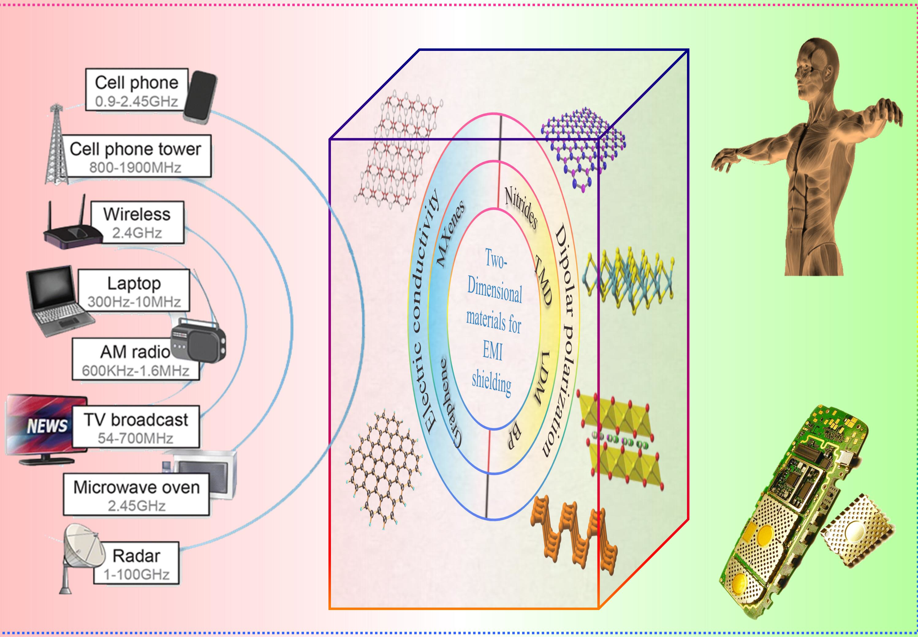
1. Introduction
2. Scope of Review
3. EMI Shielding
3.1. Concept of Green EMI Shielding
3.2. Shielding Effectiveness
Shielding Effectiveness Calculation
3.3. Shielding Measurement
- Open Field or Free Space Method;
- Shielded Box Method;
- Shielded Room Method;
- Coaxial Transmission Line Method.
3.4. Factors Effecting EMI Shielding Performance
4. Two-Dimensional Layered Shielding Materials
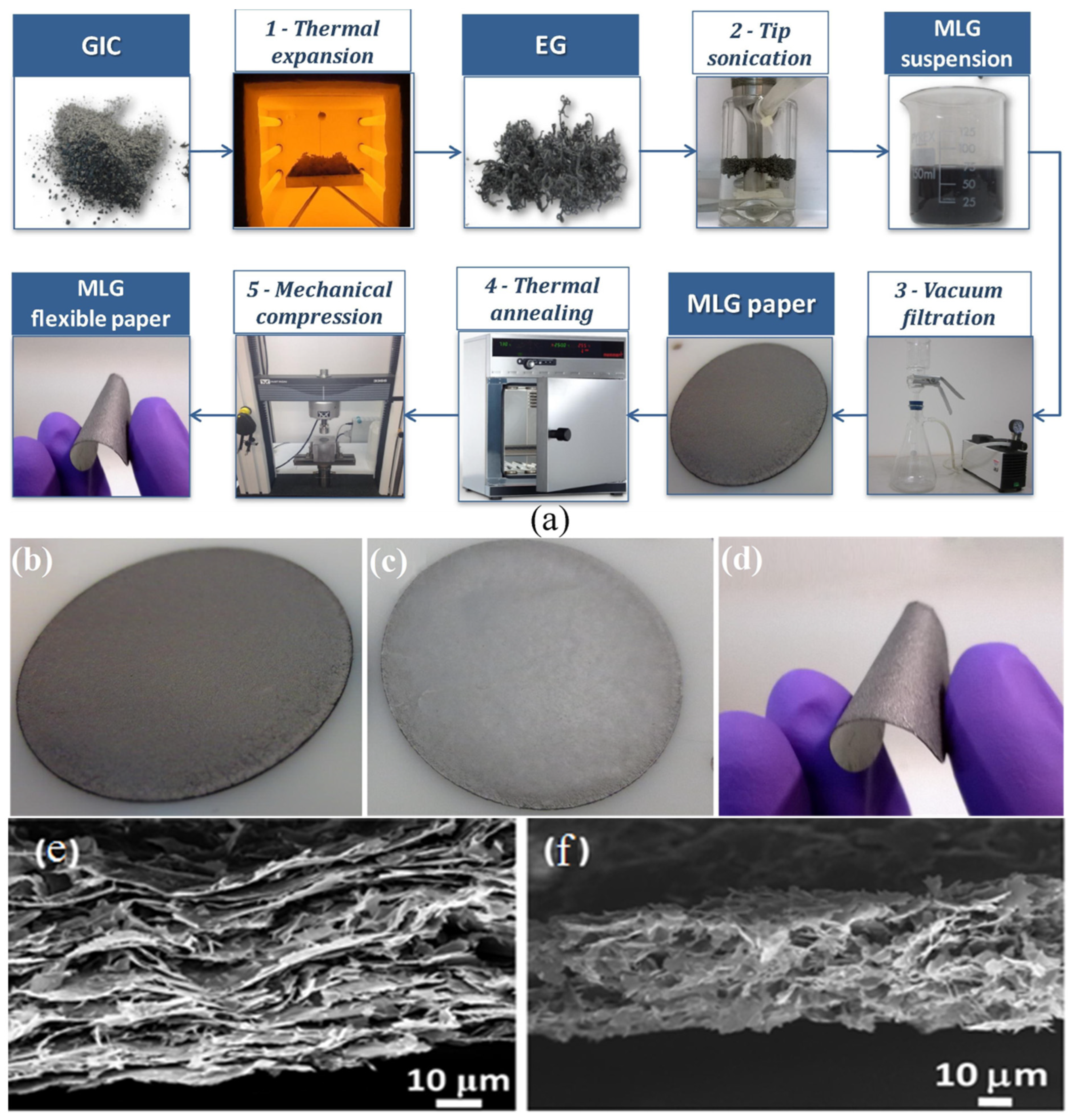
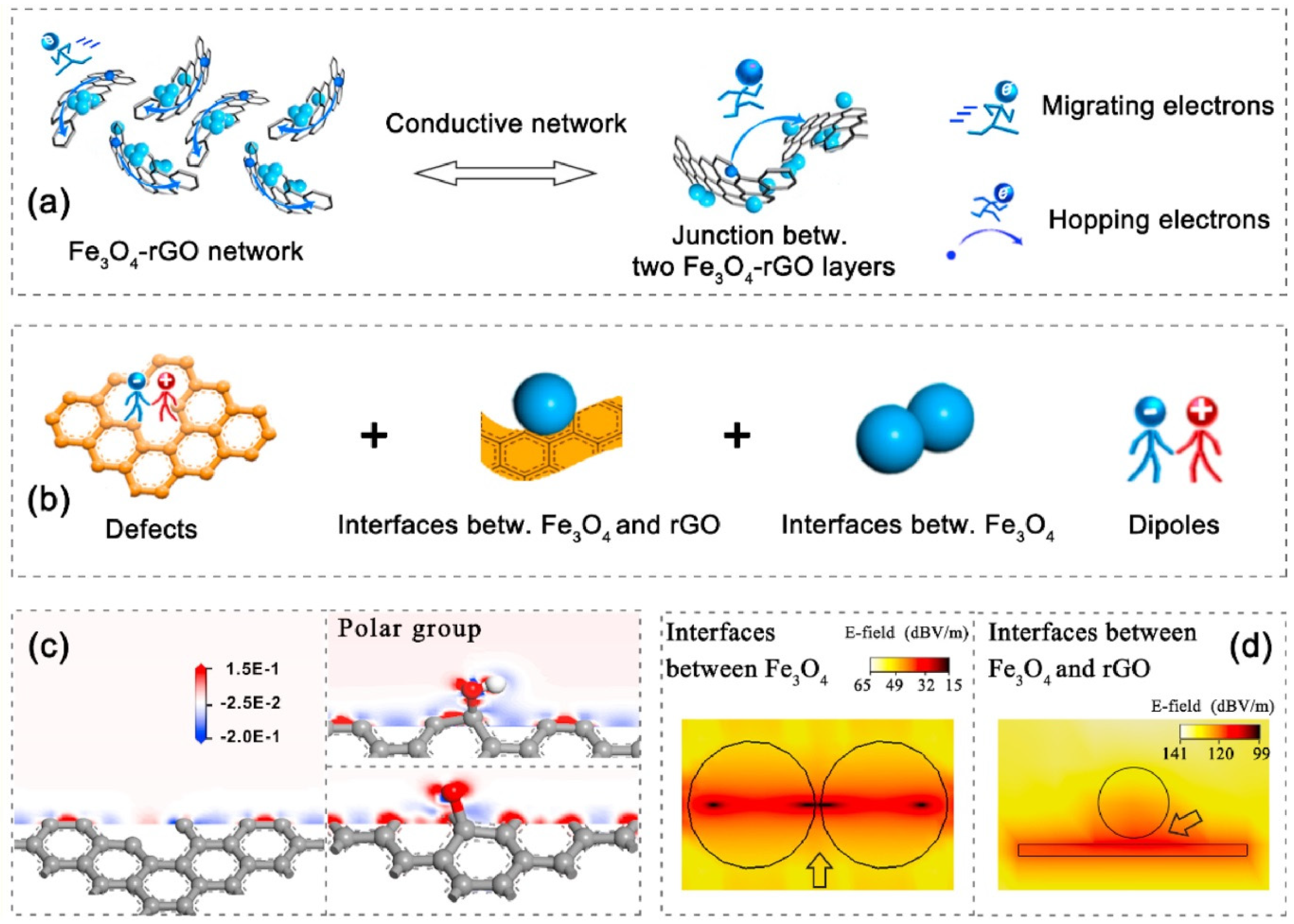
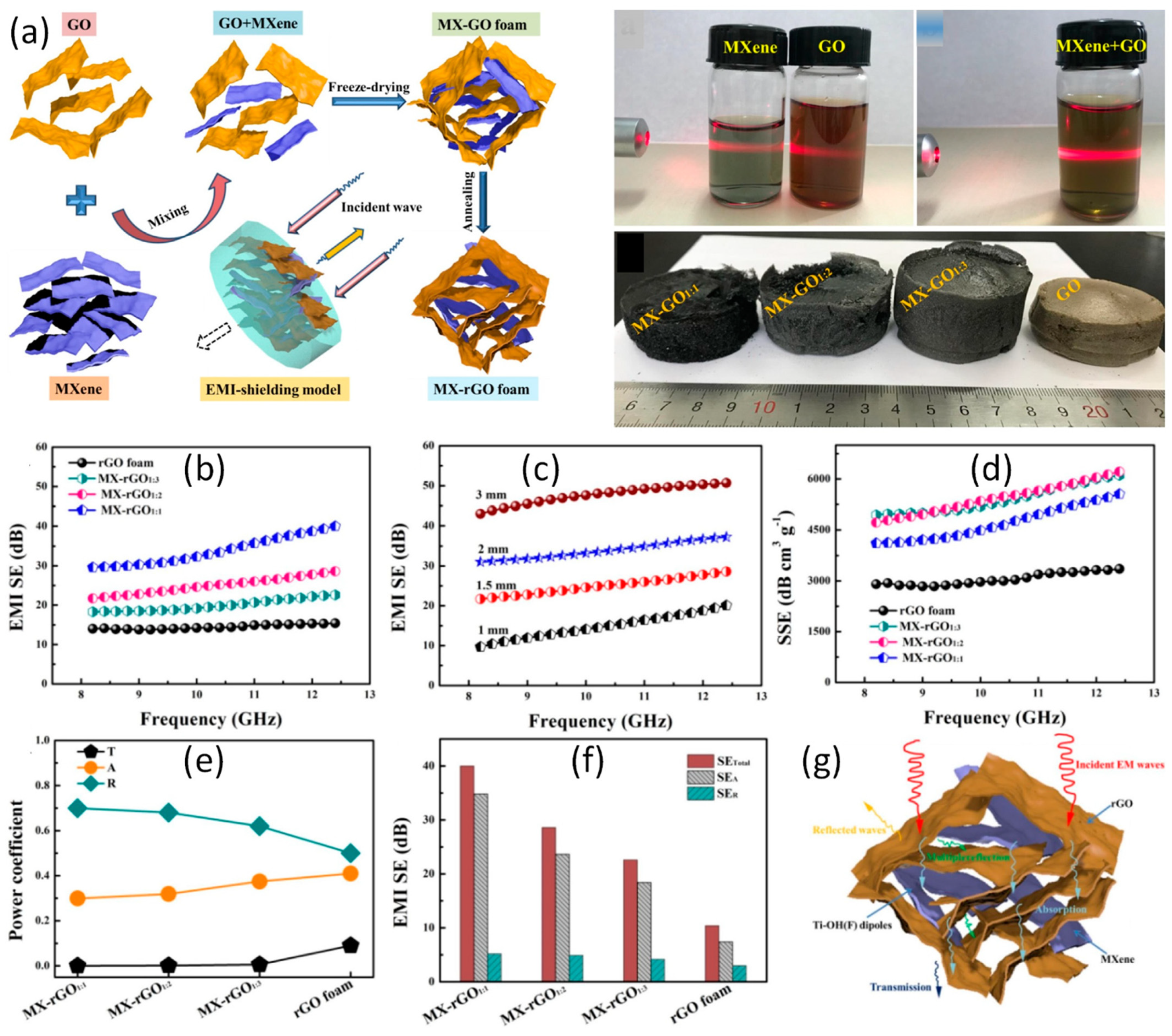
4.1. Graphene-Based Shielding Materials
4.2. D Nitrides (Boron Nitride and Graphitic Carbon Nitride)
4.3. Transition Metal Dichalcogenides
4.4. Metal-Layered Double Hydroxides
4.5. Black Phosphorus
4.6. MXenes
5. Conclusions and Future Aspects
Author Contributions
Funding
Data Availability Statement
Conflicts of Interest
References
- Balmori, A. Anthropogenic radiofrequency electromagnetic fields as an emerging threat to wildlife orientation. Sci. Total Environ. 2015, 518–519, 58–60. [Google Scholar] [CrossRef] [PubMed]
- Engels, S.; Schneider, N.L.; Lefeldt, N.; Hein, C.M.; Zapka, M.; Michalik, A.; Elbers, D.; Kittel, A.; Hore, P.J.; Mouritsen, H. Anthropogenic electromagnetic noise disrupts magnetic compass orientation in a migratory bird. Nature 2014, 509, 353–356. [Google Scholar] [CrossRef] [PubMed]
- Hutchison, Z.L.; Gill, A.B.; Sigray, P.; He, H.; King, J.W. Anthropogenic electromagnetic fields (EMF) influence the behaviour of bottom-dwelling marine species. Sci. Rep. 2020, 10, 4219. [Google Scholar] [CrossRef] [PubMed]
- Sienkiewicz, Z. Biological effects of electromagnetic fields. Power Eng. J. 1998, 12, 131–139. [Google Scholar] [CrossRef]
- Yavuz, Ö.; Ram, M.K.; Aldissi, M. Electromagnetic applications of conducting and nanocomposite materials. In The New Frontiers of Organic and Composite Nanotechnology; Elsevier: Amsterdam, The Netherlands, 2008; pp. 435–475. [Google Scholar]
- Chung, D.D. Electromagnetic interference shielding effectiveness of carbon materials. Carbon 2001, 39, 279–285. [Google Scholar] [CrossRef]
- Wang, X.; Shu, J.; Cao, W.; Zhang, M.; Yuan, J.; Cao, M. Eco-mimetic nanoarchitecture for green EMI shielding. Chem. Eng. J. 2019, 369, 1068–1077. [Google Scholar] [CrossRef]
- Zhang, M.; Cao, M.; Shu, J.; Cao, W.; Li, L.; Yuan, J. Electromagnetic absorber converting radiation for multifunction. Mater. Sci. Eng. R 2021, 145, 100627. [Google Scholar] [CrossRef]
- Cao, M.; Wang, X.; Zhang, M.; Cao, W.; Fang, X. Variable-Temperature Electron Transport and Dipole Polarization Turning Flexible Multifunctional Microsensor beyond Electrical and Optical Energy. Adv. Mater. 2020, 32, 1907156. [Google Scholar] [CrossRef]
- Zhang, D.; Liu, T.; Shu, J.; Liang, S.; Wang, X.; Cheng, J.; Wang, H.; Cao, M. Self-Assembly Construction of WS2-rGO Architecture with Green EMI Shielding. ACS Appl. Mater. Interfaces 2019, 11, 26807–26816. [Google Scholar] [CrossRef]
- Farukh, M.; Dalal, J.; Ohlan, A.; Singh, K.; Dhawan, S.K. Synthesis of Poly (3, 4-ethylene dioxythiophene) Conducting Polymer Composites for EMI Shielding Applications. Bentham Sci. 2022, 213–270. [Google Scholar]
- Dalal, J.; Gupta, A.; Lather, S.; Singh, K.; Dhawan, S.K.; Ohlan, A. Poly(3, 4-ethylene dioxythiophene) laminated reduced graphene oxide composites for effective electromagnetic interference shielding. J. Alloys Compd. 2016, 682, 52–60. [Google Scholar] [CrossRef]
- Dalal, J.; Malik, S.; Dahiya, S.; Punia, R.; Singh, K.; Maan, A.S.; Dhawan, S.K.; Ohlan, A. One pot synthesis and electromagnetic interference shielding behavior of reduced graphene oxide nanocomposites decorated with Ni0.5Co0.5Fe2O4 nanoparticles. J. Alloys Compd. 2021, 887, 161472. [Google Scholar] [CrossRef]
- Yang, Z.; Peng, H.; Wang, W.; Liu, T. Crystallization behavior of poly(ε-caprolactone)/layered double hydroxide nanocomposites. J. Appl. Polym. Sci. 2010, 116, 2658–2667. [Google Scholar] [CrossRef]
- Kumari, S.; Dalal, J.; Kumar, A.; Ohlan, A. Microwave Absorption Performance of Core–Shell rGO/Ni0.5Co0.5Fe2O4@PEDOT Composite: An Effective Approach to Reduce Electromagnetic Wave Pollution. Adv. Eng. Mater. 2022, 24, 2200635. [Google Scholar] [CrossRef]
- Cao, M.; Wang, X.; Cao, W.; Fang, X.; Wen, B.; Yuan, J. Thermally Driven Transport and Relaxation Switching Self-Powered Electromagnetic Energy Conversion. Small 2018, 14, 1800987. [Google Scholar] [CrossRef]
- Wang, X.X.; Zhang, M.; Shu, J.C.; Wen, B.; Cao, W.Q.; Cao, M.S. Thermally-tailoring dielectric “genes” in graphene-based heterostructure to manipulate electromagnetic response. Carbon 2021, 184, 136–145. [Google Scholar] [CrossRef]
- Luo, X.; Chung, D.D.L. Electromagnetic interference shielding reaching 130 dB using flexible graphite. Carbon 1996, 34, 1293–1294. [Google Scholar] [CrossRef]
- Song, Q.; Ye, F.; Yin, X.; Li, W.; Li, H.; Liu, Y.; Li, K.; Xie, K.; Li, X.; Fu, Q.; et al. Carbon Nanotube–Multilayered Graphene Edge Plane Core–Shell Hybrid Foams for Ultrahigh-Performance Electromagnetic-Interference Shielding. Adv. Mater. 2017, 29, 1701583. [Google Scholar] [CrossRef]
- Li, Y.; Shen, B.; Pei, X.; Zhang, Y.; Yi, D.; Zhai, W.; Zhang, L.; Wei, X.; Zheng, W. Ultrathin carbon foams for effective electromagnetic interference shielding. Carbon 2016, 100, 375–385. [Google Scholar] [CrossRef]
- Hong, S.K.; Kim, K.Y.; Kim, T.Y.; Kim, J.H.; Park, S.W.; Kim, J.H.; Cho, B.J. Electromagnetic interference shielding effectiveness of monolayer graphene. Nanotechnology 2012, 23, 455704. [Google Scholar] [CrossRef]
- Song, W.L.; Fan, L.Z.; Cao, M.S.; Lu, M.M.; Wang, C.Y.; Wang, J.; Chen, T.T.; Li, Y.; Hou, Z.L.; Liu, J.; et al. Facile fabrication of ultrathin graphene papers for effective electromagnetic shielding. J. Mater. Chem. C 2014, 2, 5057–5064. [Google Scholar] [CrossRef]
- Zhang, L.; Alvarez, N.T.; Zhang, M.; Haase, M.; Malik, R.; Mast, D.; Shanov, V. Preparation and characterization of graphene paper for electromagnetic interference shielding. Carbon 2015, 82, 353–359. [Google Scholar] [CrossRef]
- Paliotta, L.; De Bellis, G.; Tamburrano, A.; Marra, F.; Rinaldi, A.; Balijepalli, S.K.; Kaciulis, S.; Sarto, M.S. Highly conductive multilayer-graphene paper as a flexible lightweight electromagnetic shield. Carbon 2015, 89, 260–271. [Google Scholar] [CrossRef]
- Lu, Z.; Ma, L.; Tan, J.; Wang, H.; Ding, X. Transparent multi-layer graphene/polyethylene terephthalate structures with excellent microwave absorption and electromagnetic interference shielding performance. Nanoscale 2016, 8, 16684–16693. [Google Scholar] [CrossRef]
- Wang, L.; Jia, X.; Li, Y.; Yang, F.; Zhang, L.; Liu, L.; Ren, X.; Yang, H. Synthesis and microwave absorption property of flexible magnetic film based on graphene oxide/carbon nanotubes and Fe3O4 nanoparticles. J. Mater. Chem. A 2014, 2, 14940–14946. [Google Scholar] [CrossRef]
- Shen, B.; Zhai, W.; Zheng, W. Ultrathin Flexible Graphene Film: An Excellent Thermal Conducting Material with Efficient EMI Shielding. Adv. Funct. Mater. 2014, 24, 4542–4548. [Google Scholar] [CrossRef]
- Wen, B.; Wang, X.X.; Cao, W.Q.; Shi, H.L.; Lu, M.M.; Wang, G.; Jin, H.B.; Wang, W.Z.; Yuan, J.; Cao, M.S. Reduced graphene oxides: The thinnest and most lightweight materials with highly efficient microwave attenuation performances of the carbon world. Nanoscale 2014, 6, 5754–5761. [Google Scholar] [CrossRef]
- Yan, D.X.; Pang, H.; Li, B.; Vajtai, R.; Xu, L.; Ren, P.G.; Wang, J.H.; Li, Z.M. Structured reduced graphene oxide/polymer composites for ultra-efficient electromagnetic interference shielding. Adv. Funct. Mater. 2015, 25, 559–566. [Google Scholar] [CrossRef]
- Yan, D.X.; Ren, P.G.; Pang, H.; Fu, Q.; Yang, M.B.; Li, Z.M. Efficient electromagnetic interference shielding of lightweight graphene/polystyrene composite. J. Mater. Chem. 2012, 22, 18772–18774. [Google Scholar] [CrossRef]
- Liang, J.; Wang, Y.; Huang, Y.; Ma, Y.; Liu, Z.; Cai, J.; Zhang, C.; Gao, H.; Chen, Y. Letter to the Editor Electromagnetic interference shielding of graphene/epoxy composites. Carbon 2009, 47, 922–925. [Google Scholar] [CrossRef]
- Xi, J.; Li, Y.; Zhou, E.; Liu, Y.; Gao, W.; Guo, Y.; Ying, J.; Chen, Z.; Chen, G.; Gao, C. Graphene aerogel films with expansion enhancement effect of high-performance electromagnetic interference shielding. Carbon 2018, 135, 44–51. [Google Scholar] [CrossRef]
- Song, W.-L.; Guan, X.-T.; Fan, L.-Z.; Cao, W.-Q.; Wang, C.-Y.; Zhao, Q.-L.; Cao, M.-S. Magnetic and conductive graphene papers toward thin layers of effective electromagnetic shielding. J. Mater. Chem. A 2015, 3, 2097–2107. [Google Scholar]
- Shen, B.; Zhai, W.; Tao, M.; Ling, J.; Zheng, W. Lightweight, Multifunctional Polyetherimide/Graphene@Fe3O4 Composite Foams for Shielding of Electromagnetic Pollution. ACS Appl. Mater. Interfaces 2013, 5, 11383–11391. [Google Scholar] [CrossRef] [PubMed]
- Hsiao, S.T.; Ma, C.C.M.; Tien, H.W.; Liao, W.H.; Wang, Y.S.; Li, S.M.; Huang, Y.C. Using a non-covalent modification to prepare a high electromagnetic interference shielding performance graphene nanosheet/water-borne polyurethane composite. Carbon 2013, 60, 57–66. [Google Scholar] [CrossRef]
- Singh, A.P.; Garg, P.; Alam, F.; Singh, K.; Mathur, R.B.; Tandon, R.P.; Chandra, A.; Dhawan, S.K. Phenolic resin-based composite sheets filled with mixtures of reduced graphene oxide, γ-Fe2O3 and carbon fibers for excellent electromagnetic interference shielding in the X-band. Carbon 2012, 50, 3868–3875. [Google Scholar] [CrossRef]
- Singh, V.K.; Shukla, A.; Patra, M.K.; Saini, L.; Jani, R.K.; Vadera, S.R.; Kumar, N. Microwave absorbing properties of a thermally reduced graphene oxide/nitrile butadiene rubber composite. Carbon 2012, 50, 2202–2208. [Google Scholar] [CrossRef]
- Zhang, X.; Zhang, X.; Yang, M.; Yang, S.; Wu, H.; Guo, S.; Wang, Y. Ordered multilayer film of (graphene oxide/polymer and boron nitride/polymer) nanocomposites: An ideal EMI shielding material with excellent electrical insulation and high thermal conductivity. Compos. Sci. Technol. 2016, 136, 104–110. [Google Scholar] [CrossRef]
- Zhu, S.; Cheng, Q.; Yu, C.; Pan, X.; Zuo, X.; Liu, J.; Chen, M.; Li, W.; Li, Q.; Liu, L. Flexible Fe3O4/graphene foam/poly dimethylsiloxane composite for high-performance electromagnetic interference shielding. Compos. Sci. Technol. 2020, 189, 108012. [Google Scholar] [CrossRef]
- Cheng, K.; Li, H.; Zhu, M.; Qiu, H.; Yang, J. In situ polymerization of graphene-polyaniline@polyimide composite films with high EMI shielding and electrical properties. RSC Adv. 2020, 10, 2368–2377. [Google Scholar]
- Kang, Y.; Jiang, Z.; Ma, T.; Chu, Z.; Li, G. Hybrids of Reduced Graphene Oxide and Hexagonal Boron Nitride: Lightweight Absorbers with Tunable and Highly Efficient Microwave Attenuation Properties. ACS Appl. Mater. Interfaces 2016, 8, 32468–32476. [Google Scholar] [CrossRef]
- Yuan, J.; Li, K.; Liu, Z.; Jin, S.; Li, S.; Zhang, H. Preparation of Reduced Graphene Oxide/MnO Composite and Its Electromagnetic Wave Absorption Performance. Russ. J. Phys. Chem. A 2018, 92, 342–345. [Google Scholar] [CrossRef]
- Lv, H.; Zhang, H.; Ji, G. Development of Novel Graphene/g-C3N4 Composite with Broad-Frequency and Light-Weight Features. Part. Part. Syst. Charact. 2016, 33, 656–663. [Google Scholar] [CrossRef]
- Lv, H.; Ji, G.; Liu, W.; Zhang, H.; Du, Y. Achieving hierarchical hollow carbon@Fe@Fe3O4 nanospheres with superior microwave absorption properties and lightweight features. J. Mater. Chem. C 2015, 3, 10232–10241. [Google Scholar] [CrossRef]
- Wang, Y.; Wu, X.; Zhang, W. Synthesis and high-performance microwave absorption of graphene foam/polyaniline nanorods. Mater. Lett. 2016, 165, 71–74. [Google Scholar] [CrossRef]
- Ning, M.Q.; Lu, M.M.; Li, J.B.; Chen, Z.; Dou, Y.K.; Wang, C.Z.; Rehman, F.; Cao, M.S.; Jin, H.B. Two-dimensional nanosheets of MoS2: A promising material with high dielectric properties and microwave absorption performance. Nanoscale 2015, 7, 15734–15740. [Google Scholar] [CrossRef]
- Xie, A.; Sun, M.; Zhang, K.; Jiang, W.; Wu, F.; He, M. In situ growth of MoS2 nanosheets on reduced graphene oxide (RGO) surfaces: Interfacial enhancement of absorbing performance against electromagnetic pollution. Phys. Chem. Chem. Phys. 2016, 18, 24931–24936. [Google Scholar] [CrossRef]
- Wang, J.; Lin, X.; Zhang, R.; Chu, Z.; Huang, Z. Transition metal dichalcogenides MX2 (M=Mo, W; X=S, Se, Te) and MX2-CIP composites: Promising materials with high microwave absorption performance. J. Alloys Compd. 2018, 743, 26–35. [Google Scholar] [CrossRef]
- Zhao, Z.; Kou, K.; Zhang, L.; Wu, H. High efficiency electromagnetic wave absorber derived from transition metal layered double hydroxides. J. Colloid Interface Sci. 2020, 579, 733–740. [Google Scholar] [CrossRef] [PubMed]
- Wu, F.; Xie, A.; Sun, M.; Jiang, W.; Zhang, K. Few-layer black phosphorus: A bright future in electromagnetic absorption. Mater. Lett. 2017, 193, 30–33. [Google Scholar] [CrossRef]
- Zhang, N. Superior Microwave Absorption Properties of Ultralight Reduced Graphene Oxide/Black Phosphorus Aerogel. Nanotechnology 2018, 29, 235604. [Google Scholar]
- Zhou, T.; Ni, H.; Wang, Y.; Wu, C.; Zhang, H.; Zhang, J.; Tomsia, A.P.; Jiang, L.; Cheng, Q. Ultratough graphene–black phosphorus films. Proc. Natl. Acad. Sci. USA 2020, 117, 8727–8735. [Google Scholar] [CrossRef] [PubMed]
- Shahzad, F.; Alhabeb, M.; Hatter, C.B.; Anasori, B.; Hong, S.M.; Koo, C.M.; Gogotsi, Y. Electromagnetic interference shielding with 2D transition metal carbides (MXenes). Science 2016, 353, 1137–1140. [Google Scholar] [CrossRef] [PubMed]
- Han, M.; Yin, X.; Wu, H.; Hou, Z.; Song, C.; Li, X.; Zhang, L.; Cheng, L. Ti3C2 MXenes with Modified Surface for High-Performance Electromagnetic Absorption and Shielding in the X-Band. ACS Appl. Mater. Interfaces 2016, 8, 21011–21019. [Google Scholar] [CrossRef] [PubMed]
- Iqbal, A.; Shahzad, F.; Hantanasirisakul, K.; Kim, M.K.; Kwon, J.; Hong, J.; Kim, H.; Kim, D.; Gogotsi, Y.; Koo, C.M. Anomalous absorption of electromagnetic waves by 2D transition metal carbonitride Ti3CNTx (MXene). Science 2020, 369, 446–450. [Google Scholar] [CrossRef]
- Raagulan, K.; Braveenth, R.; Lee, L.R.; Lee, J.; Kim, B.M.; Moon, J.J.; Lee, S.B.; Chai, K.Y. Fabrication of flexible; lightweight, magnetic mushroom gills and coral-like MXene-carbon nanotube nanocomposites for EMI shielding application. Nanomaterials 2019, 9, 519. [Google Scholar] [CrossRef]
- Liu, R.; Miao, M.; Li, Y.; Zhang, J.; Cao, S.; Feng, X. Ultrathin Biomimetic Polymeric Ti3C2Tx MXene Composite Films for Electromagnetic Interference Shielding. ACS Appl. Mater. Interfaces 2018, 10, 44787–44795. [Google Scholar] [CrossRef]
- Xie, F.; Jia, F.; Zhuo, L.; Lu, Z.; Si, L.; Huang, J.; Zhang, M.; Ma, Q. Ultrathin MXene/aramid nanofiber composite paper with excellent mechanical properties for efficient electromagnetic interference shielding. Nanoscale 2019, 11, 23382–23391. [Google Scholar] [CrossRef]
- Bian, R.; He, G.; Zhi, W.; Xiang, S.; Wang, T.; Cai, D. Ultralight MXene-based aerogels with high electromagnetic interference shielding performance. J. Mater. Chem. C 2019, 7, 474–478. [Google Scholar] [CrossRef]
- Zhang, H.; Chen, J.; Ji, H.; Wang, N.; Feng, S.; Xiao, H. Electromagnetic interference shielding with absorption-dominant performance of Ti3C2TX MXene/non-woven laminated fabrics. Text. Res. J. 2021, 91, 2448–2458. [Google Scholar] [CrossRef]
- Xiang, C.; Guo, R.; Lin, S.; Jiang, S.; Lan, J.; Wang, C.; Cui, C.; Xiao, H.; Zhang, Y. Lightweight and ultrathin TiO2-Ti3C2TX/graphene film with electromagnetic interference shielding. Chem. Eng. J. 2019, 360, 1158–1166. [Google Scholar] [CrossRef]
- Abergel, D.S.L.; Apalkov, V.; Berashevich, J.; Ziegler, K.; Chakraborty, T. Properties of graphene: A theoretical perspective. Phys. A 2010, 59, 261–482. [Google Scholar] [CrossRef]
- Novoselov, K.S.; Geim, A.K.; Morozov, S.V.; Jiang, D.; Zhang, Y.; Dubonos, S.V.; Grigorieva, I.V.; Firsov, A.A. Electric field in atomically thin carbon films. Science 2004, 306, 666–669. [Google Scholar] [CrossRef] [PubMed]
- Kumaran, R.; Kumar, S.D.; Balasubramanian, N.; Alagar, M.; Subramanian, V.; Dinakaran, K. Enhanced Electromagnetic Interference Shielding in a Au–MWCNT Composite Nanostructure Dispersed PVDF Thin Films. J. Phys. Chem. C 2016, 120, 13771–13778. [Google Scholar] [CrossRef]
- Cao, M.S.; Wang, X.X.; Cao, W.Q.; Yuan, J. Ultrathin graphene: Electrical properties and highly efficient electromagnetic interference shielding. J. Mater. Chem. C 2015, 3, 6589–6599. [Google Scholar] [CrossRef]
- Zhang, M.; Wang, Y.; Huang, L.; Xu, Z.; Li, C.; Shi, G. Multifunctional Pristine Chemically Modified Graphene Films as Strong as Stainless Steel. Adv. Mater. 2015, 27, 6708–6713. [Google Scholar] [CrossRef]
- Peng, L.; Xu, Z.; Liu, Z.; Guo, Y.; Li, P.; Gao, C. Ultrahigh Thermal Conductive yet Superflexible Graphene Films. Adv. Mater. 2017, 29, 1700589. [Google Scholar] [CrossRef]
- Kuila, T.; Mishra, A.K.; Khanra, P.; Kim, N.H. Recent advances on the efficient reduction of graphene oxide and its application as energy storage electrode materials. Nanoscale 2013, 5, 52–71. [Google Scholar] [CrossRef]
- Lin, S.; Ju, S.; Zhang, J.; Shi, G.; He, Y.; Jiang, D. Ultrathin flexible graphene films with high thermal conductivity and excellent EMI shielding performance using large-sized graphene oxide flakes. RSC Adv. 2019, 9, 1419–1427. [Google Scholar] [CrossRef]
- Lai, D.; Chen, X.; Wang, G.; Xu, X.; Wang, Y. Highly conductive porous graphene film with excellent folding resilience for exceptional electromagnetic interference shielding. J. Mater. Chem. C 2020, 8, 8904–8916. [Google Scholar] [CrossRef]
- Lai, D.; Chen, X.; Wang, Y. Controllable fabrication of elastomeric and porous graphene films with superior foldable behavior and excellent electromagnetic interference shielding performance. Carbon 2020, 158, 728–737. [Google Scholar] [CrossRef]
- Guo, T.; Li, C.; Wang, Y.; Wang, Y.; Yue, J.; Tang, X.Z. A highly flexible and porous graphene-based hybrid film with superior mechanical strength for effective electromagnetic interference shielding. Appl. Phys. A Mater. Sci. Process. 2020, 126, 776. [Google Scholar] [CrossRef]
- Wang, X.; Yu, S.; Wu, Y.; Pang, H.; Yu, S.; Chen, Z.; Hou, J.; Alsaedi, A.; Hayat, T.; Wang, S. The synergistic elimination of uranium (VI) species from aqueous solution using bi-functional nanocomposite of carbon sphere and layered double hydroxide. Chem. Eng. J. 2018, 342, 321–330. [Google Scholar] [CrossRef]
- Zhang, Y.; Wang, X.; Cao, M. Confinedly implanted NiFe2O4-rGO: Cluster tailoring and highly tunable electromagnetic properties for selective-frequency microwave absorption. Nano Res. 2018, 11, 1426–1436. [Google Scholar] [CrossRef]
- Song, Q.; Ye, F.; Kong, L.; Shen, Q.; Han, L.; Feng, L.; Yu, G.; Pan, Y.; Li, H. Graphene and MXene Nanomaterials: Toward High-Performance Electromagnetic Wave Absorption in Gigahertz Band Range. Adv. Funct. Mater. 2020, 30, 2000475. [Google Scholar] [CrossRef]
- Wang, G.; Gao, Z.; Wan, G.; Lin, S.; Yang, P.; Qin, Y. High densities of magnetic nanoparticles supported on graphene fabricated by atomic layer deposition and their use as efficient synergistic microwave absorbers. Nano Res. 2014, 7, 704–716. [Google Scholar] [CrossRef]
- Dalal, J.; Lather, S.; Gupta, A.; Tripathi, R.; Maan, A.S. Reduced Graphene Oxide Functionalized Strontium Ferrite in Poly(3,4-ethylenedioxythiophene) Conducting Network: A High-Performance EMI Shielding Material. Adv. Mater. Technol. 2019, 4, 1900023. [Google Scholar] [CrossRef]
- Dalal, J.; Lather, S.; Gupta, A.; Dahiya, S.; Maan, A.S.; Dhawan, S.K.; Ohlan, A. EMI shielding properties of laminated graphene and PbTiO3 reinforced poly(3,4-ethylenedioxythiophene) nanocomposites. Compos. Sci. Technol. 2018, 165, 222–230. [Google Scholar] [CrossRef]
- Wang, Y.; Luo, S.; Ren, K.; Zhao, S.; Chen, Z.; Li, W.; Guan, J. Facile preparation of graphite particles fully coated with thin Ag shell layers for high performance conducting and electromagnetic shielding composite materials. J. Mater. Chem. C 2016, 4, 2566–2578. [Google Scholar] [CrossRef]
- Feng, J.; Hou, Y.; Wang, Y.; Li, L. Synthesis of Hierarchical ZnFe2O4@SiO2@RGO Core-Shell Microspheres for Enhanced Electromagnetic Wave Absorption. ACS Appl. Mater. Interfaces 2017, 9, 14103–14111. [Google Scholar] [CrossRef]
- Han, G.; Ma, Z.; Zhou, B.; He, C.; Wang, B.; Feng, Y.; Ma, J.; Sun, L.; Liu, C. Cellulose-based Ni-decorated graphene magnetic film for electromagnetic interference shielding. J. Colloid Interface Sci. 2021, 583, 571–578. [Google Scholar] [CrossRef]
- Qiu, B.; Zhang, X.; Xia, S.; Sun, T.; Ling, Y.; Zhou, S.; Guang, H.; Chen, Y.; Xu, Z.; Liang, M.; et al. Magnetic graphene oxide/carbon fiber composites with improved interfacial properties and electromagnetic interference shielding performance. Compos. Part A Appl. Sci. Manuf. 2022, 155, 106811. [Google Scholar] [CrossRef]
- Pakdel, A.; Zhi, C.; Bando, Y.; Golberg, D. Low-dimensional boron nitride nanomaterials. Mater. Today 2012, 15, 256–265. [Google Scholar] [CrossRef]
- Topsakal, M.; Aktürk, E.; Ciraci, S. First-principles study of two- and one-dimensional honeycomb structures of boron nitride. Phys. Rev. B Condens. Matter Mater. Phys. 2009, 79, 115442. [Google Scholar] [CrossRef]
- Ekuma, C.E.; Dobrosavljević, V.; Gunlycke, D. First-Principles-Based Method for Electron Localization: Application to Monolayer Hexagonal Boron Nitride. Phys. Rev. Lett. 2017, 118, 106404. [Google Scholar] [CrossRef] [PubMed]
- Ooi, N.; Rairkar, A.; Lindsley, L.; Adams, J.B. Electronic structure and bonding in hexagonal boron nitride. J. Phys. Condens. Matter. 2006, 18, 97–115. [Google Scholar] [CrossRef]
- Ooi, N.; Rajan, V.; Gottlieb, J.; Catherine, Y.; Adams, J.B. Structural properties of hexagonal boron nitride. Model. Simul. Mater. Sci. Eng. 2006, 14, 515–535. [Google Scholar] [CrossRef]
- Singh, P.; Babbar, V.K.; Razdan, A.; Puri, R.K.; Goel, T.C. Complex permittivity; permeability, and X-band microwave absorption of CaCoTi ferrite composites. J. Appl. Phys. 2000, 87, 4362–4366. [Google Scholar] [CrossRef]
- Habibi, N.; Pourjavadi, A. Superhydrophobic and thermally conductive carbon black/hexagonal boron nitride@Fe3O4/cellulose composite paper for electromagnetic interference shielding. Synth. Met. 2022, 285, 117008. [Google Scholar] [CrossRef]
- Tian, K.; Huang, Y.; Zhang, C.; Shu, R.; Zhu, J.; Liu, Y.; Chen, Z.; Li, C.; Liu, X. In-situ synthesis of graphite carbon nitride nanotubes/Cobalt@Carbon with castor-fruit-like structure as high-efficiency electromagnetic wave absorbers. J. Colloid Interface Sci. 2022, 620, 454–464. [Google Scholar] [CrossRef]
- Yoffe, A.D. Electronic properties of low dimensional solids: The physics and chemistry of layer type transition metal dichalcogenides and their intercalate complexes. Solid State Ionics 1990, 39, 1–7. [Google Scholar] [CrossRef]
- Doran, N.J. Electronic structure and band theory of transition metal dichalcogenides. Phys. B+C 1980, 99, 227–237. [Google Scholar] [CrossRef]
- Chhowalla, M.; Shin, H.S.; Eda, G.; Li, L.J.; Loh, K.P.; Zhang, H. The chemistry of two-dimensional layered transition metal dichalcogenide nanosheets. Nat. Chem. 2013, 5, 263–275. [Google Scholar] [CrossRef] [PubMed]
- Uddin, A.; Khatoon, R.; Estevez, D.; Salem, M.; Ali, A.; Attique, S.; Lu, J.; Qin, F.X. Waste paper cellulose based-MoS2 hybrid composites: Towards sustainable green shielding. Mater. Today Commun. 2022, 31, 103858. [Google Scholar] [CrossRef]
- Prasad, J.; Singh, A.K.; Tomar, M.; Gupta, V.; Singh, K. Hydrothermal synthesis of micro-flower like morphology aluminum-doped MoS2/rGO nanohybrids for high efficient electromagnetic wave shielding materials. Ceram. Int. 2021, 47, 15648–15660. [Google Scholar] [CrossRef]
- Evans, D.G.; Slade, R.C.T. Structural aspects of layered double hydroxides. In Layered Double Hydroxides. Structure and Bonding; Springer: Berlin/Heidelberg, Germany, 2005; pp. 1–87. [Google Scholar]
- Jamil, S.; Alvi, A.R.; Khan, S.R.; Janjua, M.R.S.A. Layered Double Hydroxides (LDHs): Synthesis & Applications. Prog. Chem. 2019, 31, 394–412. [Google Scholar]
- Bukhtiyarova, M.V. A review on effect of synthesis conditions on the formation of layered double hydroxides. J. Solid State Chem. 2019, 269, 494–506. [Google Scholar] [CrossRef]
- Quan, B.; Liang, X.; Ji, G.; Lv, J.; Dai, S.S.; Xu, G.; Du, Y. Laminated graphene oxide-supported high-efficiency microwave absorber fabricated by an in situ growth approach. Carbon 2018, 129, 310–320. [Google Scholar] [CrossRef]
- Lu, Y.; Yang, P.; Li, Y.; Wen, D.; Luo, J.; Wang, S.; Wu, F.; Fang, L.; Pang, Y. A Facile Synthesis of NiFe-Layered Double Hydroxide and Mixed Metal Oxide with Excellent Microwave Absorption Properties. Molecules 2021, 26, 5046. [Google Scholar] [CrossRef]
- Gan, F.; Yao, Q.; Deng, J.; Wang, F.; Cheng, L.; Chen, Y.; Zhou, H.; Zhong, Y.; Yang, H.; Zhao, Y. Layered double hydroxides derived 3D flower-like FeNi@C microspheres as lightweight and high-efficient electromagnetic wave absorber. Carbon 2022, 196, 639–648. [Google Scholar] [CrossRef]
- Bridgman, P.W. Two new modifications of phosphorus. J. Am. Chem. Soc. 1914, 36, 1344–1363. [Google Scholar] [CrossRef]
- Bridgman, P.W. Further note on black phosphorus. J. Am. Chem. Soc. 1916, 38, 609–612. [Google Scholar] [CrossRef]
- Jacobs, R.B. Phosphorus at High Temperatures and Pressures. J. Chem. Phys. 1937, 5, 945–953. [Google Scholar] [CrossRef]
- Keyes, R.W. The electrical properties of black phosphorus. Phys. Rev. 1953, 92, 580–584. [Google Scholar] [CrossRef]
- Naguib, M.; Kurtoglu, M.; Presser, V.; Lu, J.; Niu, J.; Heon, M.; Hultman, L.; Gogotsi, Y.; Barsoum, M.W. Two-dimensional nanocrystals produced by exfoliation of Ti3AlC2. Adv. Mater. 2011, 23, 4248–4253. [Google Scholar]
- Naguib, M.; Mochalin, V.N.; Barsoum, M.W.; Gogotsi, Y. 25th anniversary article: MXenes: A new family of two-dimensional materials. Adv. Mater. 2014, 26, 992–1005. [Google Scholar] [CrossRef]
- Verger, L.; Natu, V.; Carey, M.; Barsoum, M.W. MXenes: An introduction of their synthesis, select properties, and applications. Trends Chem. 2019, 1, 656–669. [Google Scholar]
- Han, M.; Yin, X.; Hantanasirisakul, K.; Li, X.; Iqbal, A.; Hatter, C.B.; Anasori, B.; Koo, C.M.; Torita, T.; Soda, Y.; et al. Anisotropic MXene Aerogels with a Mechanically Tunable Ratio of Electromagnetic Wave Reflection to Absorption. Adv. Opt. Mater. 2019, 7, 1900267. [Google Scholar] [CrossRef]
- Lee, S.H.; Yu, S.; Shahzad, F.; Kim, W.N.; Park, C.; Hong, S.M.; Koo, C.M. Density-tunable lightweight polymer composites with dual-functional ability of efficient EMI shielding and heat dissipation. Nanoscale 2017, 9, 13432–13440. [Google Scholar]
- Wang, L.; Chen, L.; Song, P.; Liang, C.; Lu, Y.; Qiu, H.; Zhang, Y.; Kong, J.; Gu, J. Fabrication on the annealed Ti3C2Tx MXene/Epoxy nanocomposites for electromagnetic interference shielding application. Compos. Part B Eng. 2019, 171, 111–118. [Google Scholar] [CrossRef]
- Xu, H.; Yin, X.; Li, X.; Li, M.; Liang, S.; Zhang, L.; Cheng, L. Lightweight Ti2CTx MXene/Poly(vinyl alcohol) Composite Foams for Electromagnetic Wave Shielding with Absorption-Dominated Feature. ACS Appl. Mater. Interfaces 2019, 11, 10198–10207. [Google Scholar]
- Wei, H.; Dong, J.; Fang, X.; Zheng, W.; Sun, Y.; Qian, Y.; Jiang, Z.; Huang, Y. Ti3C2Tx MXene/polyaniline (PANI) sandwich intercalation structure composites constructed for microwave absorption. Compos. Sci. Technol. 2019, 169, 52–59. [Google Scholar] [CrossRef]
- Cao, W.; Ma, C.; Tan, S.; Ma, M.; Wan, P.; Chen, F. Ultrathin and Flexible CNTs/MXene/Cellulose Nanofibrils Composite Paper for Electromagnetic Interference Shielding. Nano-Micro Lett. 2019, 11, 72. [Google Scholar] [CrossRef] [PubMed]
- Jin, X.; Wang, J.; Dai, L.; Liu, X.; Li, L.; Yang, Y.; Cao, Y.; Wang, W.; Wu, H.; Guo, S. Flame-retardant poly(vinyl alcohol)/MXene multilayered films with outstanding electromagnetic interference shielding and thermal conductive performances. Chem. Eng. J. 2020, 380, 122475. [Google Scholar] [CrossRef]
- Fan, Z.; Wang, D.; Yuan, Y.; Wang, Y.; Cheng, Z.; Liu, Y.; Xie, Z. Lightweight and conductive MXene/graphene hybrid foam for superior electromagnetic interference shielding. Chem. Eng. J. 2020, 381, 122696. [Google Scholar] [CrossRef]
- Zhang, Y.; Ruan, K.; Shi, X.; Qiu, H.; Pan, Y.; Yan, Y.; Gu, J. Ti3C2Tx/rGO porous composite films with superior electromagnetic interference shielding performances. Carbon 2021, 175, 271–280. [Google Scholar] [CrossRef]
- Liu, J.; Zhang, H.B.; Sun, R.; Liu, Y.; Liu, Z.; Zhou, A.; Yu, Z.Z. Hydrophobic, Flexible, and Lightweight MXene Foams for High-Performance Electromagnetic-Interference Shielding. Adv. Mater. 2017, 29, 1702367. [Google Scholar] [CrossRef]
- Han, M.; Yin, X.; Li, X.; Anasori, B.; Zhang, L.; Cheng, L.; Gogotsi, Y. Laminated and Two-Dimensional Carbon-Supported Microwave Absorbers Derived from MXenes. ACS Appl. Mater. Interfaces 2017, 9, 20038–20045. [Google Scholar] [CrossRef]
- Li, X.; Yin, X.; Han, M.; Song, C.; Sun, X.; Xu, H.; Cheng, L.; Zhang, L. A controllable heterogeneous structure and electromagnetic wave absorption properties of Ti2CT: X MXene. J. Mater. Chem. C 2017, 5, 7621–7628. [Google Scholar] [CrossRef]
- Choi, G.; Shahzad, F.; Bahk, Y.M.; Jhon, Y.M.; Park, H.; Alhabeb, M.; Anasori, B.; Kim, D.S.; Koo, C.M.; Gogotsi, Y.; et al. Enhanced Terahertz Shielding of MXenes with Nano-Metamaterials. Adv. Opt. Mater. 2018, 6, 1701076. [Google Scholar] [CrossRef]
- Han, M.; Shuck, C.E.; Rakhmanov, R.; Parchment, D.; Anasori, B.; Koo, C.M.; Friedman, G.; Gogotsi, Y. Beyond Ti3C2Tx: MXenes for Electromagnetic Interference Shielding. ACS Nano 2020, 14, 5008–5016. [Google Scholar] [CrossRef]
- Nguyen, V.T.; Min, B.K.; Yi, Y.; Kim, S.J.; Choi, C.G. MXene(Ti3C2TX)/graphene/PDMS composites for multifunctional broadband electromagnetic interference shielding skins. Chem. Eng. J. 2020, 393, 124608. [Google Scholar] [CrossRef]
- Cheng, H.; Pan, Y.; Chen, Q.; Che, R.; Zheng, G.; Liu, C.; Shen, C.; Liu, X. Ultrathin flexible poly(vinylidene fluoride)/MXene/silver nanowire film with outstanding specific EMI shielding and high heat dissipation. Adv. Compos. Hybrid Mater. 2021, 4, 505–513. [Google Scholar] [CrossRef]
- Qi, F.; Wang, L.; Zhang, Y.; Ma, Z.; Qiu, H.; Gu, J. Robust Ti3C2Tx MXene/starch derived carbon foam composites for superior EMI shielding and thermal insulation. Mater. Today Phys. 2021, 21, 100512. [Google Scholar] [CrossRef]
- Cao, Y.; Zeng, Z.; Huang, D.; Chen, Y.; Zhang, L.; Sheng, X. Multifunctional phase change composites based on biomass/MXene-derived hybrid scaffolds for excellent electromagnetic interference shielding and superior solar/electro-thermal energy storage. Nano Res. 2022, 15, 8524–8535. [Google Scholar] [CrossRef]


| Materials | Loading | Thickness (mm) | Frequency (GHz) | EMI SE (dB) | Ref. |
|---|---|---|---|---|---|
| Flexible Graphite | Bulk | 3.1 | 1–2 | 130 | [18] |
| Carbon foam | 20 wt% | 0.8 | 8.2–12.4 | 24 | [19] |
| Ultrathin carbon foam | Massive | 0.024 | 8–12 | 24 | [20] |
| Monolayer graphene | Massive | 0.34 | 2.2–7 | 2.27 | [21] |
| Graphene paper | Massive | 0.3 | 8.2–12.4 | 46.3 | [22] |
| Graphene paper | Massive | 0.05 | 8–12 | 60 | [23] |
| Multilayer graphene sheet | Massive | 0.018 | 0.1–18 | 55 | [24] |
| GN/PET film | __ | 1.50 | 18–26.5 | 55.11 | [25] |
| GO/CNT-Fe3O4 | 67 wt% | 2.0 | 12 | −19.74 (RL) | [26] |
| rGO film | Bulk | 0.0084 | 8–12 | 19.1 | [27] |
| rGO/wax | 20 wt% | 2.0 | 2–18 | 29 | [28] |
| rGO/PS composite | 7wt% | 2.5 | 8.2–12.4 | 45.1 | [29] |
| rGO/PS foam | 30 wt% | 2.5 | 8.2–12.4 | 30 | [30] |
| rGO/epoxy | 15 wt% | 2.0 | 8.2–12.4 | 21 | [31] |
| Graphene aerogel film | Bulk | 1.4 | 0.1–3 | 135 | [32] |
| Fe3O4/GN | Bulk | 0.3 mm | 8.2–12.4 | 21 | [33] |
| rGO/PEI foam | 5 wt% | 2.5 | 8.2–12.4 | 17.8 | [34] |
| rGO/WPU | 7.7 wt% | 2.0 | 8.2–12.4 | 32 | [35] |
| rGO/phenolic | 70 wt% | 0.3 | 8.2–12.4 | 43.4 | [36] |
| rGO/NBR | 10 wt% | 3.0 | 7.5–12 | 57 | [37] |
| Multilayer f-GO/polymer | 35 wt% | 0.235 | 8.2–12.4 | 37.92 | [38] |
| Fe3O4/GN/PDMS | Bulk | 1.0 | 8.2–12.4 | 32.4 | [39] |
| Gr-PANI@PI | 40 wt% | 0.04 | 8.2–12.4 | 21.3 | [40] |
| rGO/h-BN | 25 wt% | 1.6 | 15.3 | −40.5 (RL) | [41] |
| rGO/MnO | Bulk | 2.0 | 11.5–16.4 | −38.9 (RL) | [42] |
| GN/CN | 10 wt% | 1.5 | 12.8–18 | −29.6 (RL) | [43] |
| Carbon@Fe@Fe3O4 | Bulk | 1.5 | 8.6–13.8 | −40 (RL) | [44] |
| GF/PANI nanorods | Bulk | 2 | 13.8 | −52.5 (RL) | [45] |
| MoS2-NS/wax | 60 wt% | 2.4 | 9.6–13.76 | −38.42 (RL) | [46] |
| rGO/MoS2/wax | 20 wt% | 2.5 | 13.48 | −60 (RL) | [47] |
| MoSe2/paraffin | 80 wt% | 2.56 | 8.48 | −60.23 (RL) | [48] |
| WSe2-CIP/paraffin | 80 wt% | 1.86 | 12.3 | −68.14 (RL) | [48] |
| FeCo-LDHs | Bulk | 2.0 | 12.24–16.72 | −29.9 (RL) | [49] |
| FL-BP | 30 wt% | 2.5 | 12–18 | −46.5 (RL) | [50] |
| rGO/BP aerogel | Bulk | 2.53 | 10 | −46.9 (RL) | [51] |
| rGO/BP-AD films | 50 wt% | 0.005 | 8 | 29.7 | [52] |
| Ti3C2Tx free-standing film | Bulk | 0.045 | 8.2–12.4 | 92 | [53] |
| Ti3C2Tx/SA | 90 wt% | 0.008 | 8.2–12.4 | 57 | [53] |
| Ti3C2Tx/SA | Bulk | 0.011 | 8.2–12.4 | 68 | [53] |
| Mo2Ti2C3Tx film | Bulk | 0.0035 | 8.2–12.4 | 26 | [53] |
| Annealed Ti3C2Tx | 50 wt% | 1.7 | 11.6 | −48.4 (RL) | [54] |
| Ti3C2 MXene/wax | 90 wt% | 1 | 8.2–12.4 | 76.1 | [54] |
| Ti3CNTx | Bulk | 0.04 | 8.2–12.4 | 116 | [55] |
| Ti3C2TxCS | Bulk | 0.386 | 8.2–12.4 | 50.5 | [56] |
| Ti3C2Tx/PEDOT: PSS | Bulk | 0.007 | 8.2–12.4 | 42.5 | [57] |
| Ti3C2Tx/PEDOT: PSS | 87.5 wt% | 0.011 | 8.2–12.4 | 42.1 | [57] |
| d-Ti3C2Tx/ANF | 90 wt% | 0.015 | 8.2–12.4 | 32.84 | [58] |
| Ti3C2Tx aerogel | Bulk | 2.0 | 8.2–12.4 | 75 | [59] |
| Calcium alginate/Ti3C2Tx | Bulk | 3.17 | 12.4 | 25.26 | [60] |
| TiO2-Ti3C2Tx/GO | Bulk | 0.0091 | 12.4 | 28.2 | [61] |
Disclaimer/Publisher’s Note: The statements, opinions and data contained in all publications are solely those of the individual author(s) and contributor(s) and not of MDPI and/or the editor(s). MDPI and/or the editor(s) disclaim responsibility for any injury to people or property resulting from any ideas, methods, instructions or products referred to in the content. |
© 2023 by the authors. Licensee MDPI, Basel, Switzerland. This article is an open access article distributed under the terms and conditions of the Creative Commons Attribution (CC BY) license (https://creativecommons.org/licenses/by/4.0/).
Share and Cite
Kumari, S.; Dalal, J.; Kumar, V.; Kumar, A.; Ohlan, A. Emerging Two-Dimensional Materials for Electromagnetic Interference Shielding Application. Int. J. Mol. Sci. 2023, 24, 12267. https://doi.org/10.3390/ijms241512267
Kumari S, Dalal J, Kumar V, Kumar A, Ohlan A. Emerging Two-Dimensional Materials for Electromagnetic Interference Shielding Application. International Journal of Molecular Sciences. 2023; 24(15):12267. https://doi.org/10.3390/ijms241512267
Chicago/Turabian StyleKumari, Suman, Jasvir Dalal, Vibhor Kumar, Anand Kumar, and Anil Ohlan. 2023. "Emerging Two-Dimensional Materials for Electromagnetic Interference Shielding Application" International Journal of Molecular Sciences 24, no. 15: 12267. https://doi.org/10.3390/ijms241512267
APA StyleKumari, S., Dalal, J., Kumar, V., Kumar, A., & Ohlan, A. (2023). Emerging Two-Dimensional Materials for Electromagnetic Interference Shielding Application. International Journal of Molecular Sciences, 24(15), 12267. https://doi.org/10.3390/ijms241512267