Abstract
In this study, n-type MoS2 monolayer flakes are grown through chemical vapor deposition (CVD), and a p-type Cu2O thin film is grown via electrochemical deposition. The crystal structure of the grown MoS2 flakes is analyzed through transmission electron microscopy. The monolayer structure of the MoS2 flakes is verified with Raman spectroscopy, multiphoton excitation microscopy, atomic force microscopy, and photoluminescence (PL) measurements. After the preliminary processing of the grown MoS2 flakes, the sample is then transferred onto a Cu2O thin film to complete a p-n heterogeneous structure. Data are confirmed via scanning electron microscopy, SHG, and Raman mapping measurements. The luminous energy gap between the two materials is examined through PL measurements. Results reveal that the thickness of the single-layer MoS2 film is 0.7 nm. PL mapping shows a micro signal generated at the 627 nm wavelength, which belongs to the B2 excitons of MoS2 and tends to increase gradually when it approaches 670 nm. Finally, the biosensor is used to detect lung cancer cell types in hydroplegia significantly reducing the current busy procedures and longer waiting time for detection. The results suggest that the fabricated sensor is highly sensitive to the change in the photocurrent with the number of each cell, the linear regression of the three cell types is as high as 99%. By measuring the slope of the photocurrent, we can identify the type of cells and the number of cells.
1. Introduction
Molybdenum disulfide (MoS2) is one of the two-dimensional (2D) transition metal chalcogenides that have been studied recently [1,2,3,4,5,6]. Materials related to nanometer-scale electronic and optoelectronic components, such as field-effect transistors, prospective memory components, light-emitting diodes (LED), and sensors, have been manufactured because of the excellent spin-valley coupling and flexural and optoelectronic properties of MoS2 [7,8,9,10,11,12,13,14,15,16,17,18,19]. However, MoS2 is a layered structure, which has good lubricity, resistance to pressure, and wear resistance, and is mostly used as solid lubricant [20]. It is used in equipment operating under high-speed, heavy-load, high-temperature, and chemical corrosive conditions. MoS2 is a black hexagonal crystal structure with silver-gray luster, its Moiré mass is 160.07 g/mol, density is 5.06 g/cm3, and melting point is 1185 °C. MoS2 itself is insoluble in water, generally insoluble in other acids, alkalis, and organic solvents. However, at 400 °C, oxidation occurs slowly, and molybdenum trioxide (MoO3) gradually forms. PN heterostructures have been widely used in the semiconductor industry; as a typical P-type semiconductor, Cu2O is considered to be the most effective material [21]. With these characteristics, Cu2O can be effectively used as an absorption layer in the visible wavelength range [22,23,24,25]. In a bulk MoS2 semiconductor, an indirect energy gap of 1.2 eV between the G- and S-point conduction bands, and a single-layer MoS2 semiconductor has a direct energy gap of 1.84 eV. Studies on light absorption, light reflection, and light excitation spectroscopy have evolved from bulk materials to single-layer TMDs [26]. In 2014, Yu-Fei Zhao et al. used a simple chemical synthesis method to cover MoS2 successfully on p-Cu2O semiconductors for high-efficiency solar hydrogen production [21]. In 2016, Xinne Zhao et al. assembled Cu2O nanoparticles and MoS2 nanosheets with a 2D planar structure into a 3D MoS2/Cu2O porous nanocomposite through hydrothermal synthesis [27,28]. In 2017, Linxia Fang et al. successfully decorated Cu2O nanoparticles on flower-like MoS2 and used them for non-enzymatic current detection in glucose. This structure has Cu2O nanoparticles dispersed in MoS2 [29]. Gang Li et al. reported the hydrothermal synthesis of MoS2/Cu2O nanocomposites with a tunable heterojunction to enhance the photochemical activity and stability of visible light [30]. The lack of energy gap of graphene in two-dimensional materials has shifted the focus on two-dimensional transition metal dichalcogenides (TMDs) with different energy gaps obtained by changing the number of layers. In the review of previous studies on MoS2/Cu2O, MoS2/Cu2O has high-performance photocatalysis, excellent electrocatalysis, strong stability, reproducibility, and high selectivity for non-MEI sensors. This structure can be used as a hydrogen oxide biosensor for environmental engineering applications, such as energy storage and water purification. It can also be used as a non-MEI current detection in glucose oxidation. It is better for the signal interference of uric acid, dopamine, and ascorbic acid. Apart from inorganic biosensors, organic materials are also getting attention in the last few years. Some biosensors using poly(methylene blue) (PMB), poly(alizarin yellow R), poly(azure A), poly(azure B), poly(azure C), poly(brilliant cresyl blue), and poly(thionine) has been widely studied and reported [31,32,33,34,35,36,37]. Even though these biosensors have good selectivity, their disadvantages include instability, cost, and a need for a mediator in some cases [38]. On the other hand, in recent years due to the excellent electrochemical properties of Cu2O, much research has been conducted towards its application as a sensor [39,40,41,42]. MoS2 which has a similar structure to graphene due to its conductivity and good electrical and chemical properties has been widely reported to be employed in numerous biosensors [43,44,45].
Hence, in this research, a new MoS2/Cu2O PN heterojunction structure, can reduce the predominant disadvantage of noise interference to the detection signal through different growth methods, material special characteristics, and the structure itself. This MoS2/Cu2O structure is applied to a sensor for cancer cells with different canceration levels. In this study, CVD is conducted for single-layer MoS2 to obtain large-area and uniform MoS2 films. Several measurement techniques, including Raman mapping, are used to check the number of layers. Atomic force microscopy (AFM) is employed for thickness analysis and scanning electron microscopy (SEM) is utilized to observe surface morphology. X-ray diffraction (XRD; Figure S1 for XRD) is conducted to measure whether a signal appears, and transmission electron microscopy (TM; Figure S4) is performed to determine the direction of the crystal lattice. However, studies on the synthesis of semiconductor materials and nanostructures have also been carried out. During the research, Cu2O nanostructures have been successfully fabricated through electrochemical deposition. The major application of this heterostructure is to develop a low-cost and rapid way to detect lung cancer cell types in hydroplegia by fabricating a PEC biosensor that is highly sensitive to lung cancer cells significantly reducing the current busy procedures and longer waiting time for detection.
2. Materials and Methods
The glass substrate used in the experiment was indium tin oxide (ITO) for Cu2O electroplating. The resistance of the ITO surface was 7 Ω, and the thickness of the coating was 200 nm. All the chemicals used were all American Chemical Society (ACS) and guaranteed reagent (GR) to avoid the failure of results because of insufficient purity or residual impurities in the grown crystals, especially low-chlorine Sigma-Aldrich (Burlington, MA, USA) 98+% for sodium hydroxide because the solution of Cu2O deposition was susceptible to the influence of chloride ions to produce copper chloride precipitation.
2.1. Process and Steps of Electrochemical Cu2O Growth
2.1.1. Substrate and Electrolysis Pretreatment
Cu2O was prepared through electrochemical deposition, and the substrate used was a 2 cm × 2 cm transparent conductive film made of ITO for Cu2O electroplating (Supplementary Section S1.1 for the Material characteristics of Cu2O). P-type Cu2O has a small energy gap of 2.0 eV, which was a suitable conduction band [46,47]. Acetone, methanol, isopropanol, and deionized water were used to reduce the impurities, such as dust, oil stains, or residues, on the electrode surface after ITO plating. The adhesion of impurity contamination also improved the stability of film growth to obtain a higher-quality Cu2O film (Supplementary Section S3 for the List of substrates, organic solvents, gases, and chemicals used to grow Cu2O and MoS2). In the cleaning steps, the electrode surface was first cleaned with acetone in an ultrasonic oscillator for 10 min to dissolve and remove surface oil stains or other organic impurities. After the specimen was shaken and washed with acetone, it was rinsed with methanol in an ultrasonic oscillator for 10 min to dissolve and remove residual copper contamination on the surface. Isopropanol was used for cleaning in an ultrasonic oscillator for 10 min to dissolve and remove surface oil stains or other organic impurities. The glass substrate was soaked in deionized water with a resistivity of 18.2 M W·cm (25 °C), and an ultrasonic oscillator was used for 10 min to remove residual organic solvents. The sample was taken out, and a high-pressure nitrogen gun was used to remove the moisture on the surface of the ITO glass substrate. The ITO glass substrate was baked in an oven at 100 °C for 30 min to remove the residual moisture on the substrate and placed in a clean moisture-proof box for later use. The cut graphite rods with a diameter of 1 cm and a length of 18 cm were subjected to electrochemical Cu2O deposition. The main purpose of cleaning the electrodes of the graphite rods was to reduce impurities, such as dust, oil stains, and residual powder, on the electrode surface during graphite rod production. External impurities contaminated Cu2O electrolytic deposition and improved film growth stability. For cleaning, the graphite rod was soaked in 1 M sodium hydroxide solution and washed with ultrasonic vibration for 30 min to remove grease and organic pollutants adsorbed on the surface. The surface of the graphite rod was ground with sandpaper and rinsed with deionized water during grinding to remove the powder remaining in the graphite rod manufacturing. The graphite rod was soaked in deionized water and shaken for 30 min with ultrasonic cleaning to reduce the residual impurities on the surface. The graphite rod was baked in an oven at 100 °C for 30 min to remove the surface moisture and placed in a moisture-proof box to complete the pretreatment of the graphite electrode.
2.1.2. Preparation of Cu2O Film
A Cu2O thin film was prepared for electrochemical deposition to grow a highly uniform thin film on the ITO glass substrate (Supplementary Section S1.2 for Cu2O Synthesis). The electrolyte was made of 0.4 M copper sulfate powder (CuSO4), 85% lactic acid, and 5 M sodium hydroxide (NaOH) prepared into a 1000 c.c. aqueous solution. The pH could be adjusted to 10, 11, and 12 through the amount of sodium hydroxide, which was measured in real time by a portable Starter300 pH meter (ST300). A DC power supply (MOTECH LPS505N) was used to power the two-pole electrochemical deposition system equipment in which the positive electrode was a graphite rod, and the negative electrode was connected to the ITO glass substrate (Supplementary Section S2.1 for the electrochemical deposition system). The temperature of the growing electrolyte was controlled at 60 °C to ensure that the lactic acid works. The deposition time was fixed at 30 min to achieve high quality and uniformity. At the end of the film, the sample was washed with deionized water, and the surface moisture was removed with a high-pressure nitrogen gun for subsequent experiments.
2.1.3. Cu2O Grinding
A plane grinder was widely used for the single-sided grinding and polishing of various materials, such as LED sapphire substrates, optical glass wafers, quartz wafers, silicon wafers, germanium wafers, molds, light guide plates, and optical skewer joints. The Cu2O thin film was processed by grinding to smoothen the Cu2O surface and facilitate the subsequent transfer of MoS2 while maintaining the integrity of the morphological characteristics of MoS2 and reducing the transfer failure rate. The rotation speed of the grinder was controlled at the minimum, and the time was set at 1 h. Considering Cu2O was a thin film at the micrometer scale, we chose the micro grade at the scale of a diamond polishing sheet.
2.1.4. Experimental Materials and Drug Specifications of MoS2
The substrate used to grow MoS2 was silicon dioxide (SiO2) for chemical vapor deposition (CVD; Supplementary Section S1.2 for obtaining MoS2 layers). The thickness of the chosen silicon wafer (100) crystal plane was 300 nm. The purity of sulfur powder (S) and molybdenum oxide (MoO3) powder was 99.98% and 99.95%, respectively, to avoid impurities that affect the CVD or the remaining impurities of grown single crystals. The quartz tubes and ceramic crucibles in the tubular thermal tubes were cleaned with aqua regia. The concentrations of nitric acid and hydrochloric acid were 37% and 68–69%, respectively, to avoid the adhesion of impurities from the previous growth during cleaning, which affects the experimental parameters and reproducibility of the next growth of monolayer MoS2.
2.2. Process and Steps of CVD-Grown MoS2
The majority of 2D material layer identification studies focus on film synthesis using mechanical stripping [48,49,50]. Most 2D material layer identification studies have focused on film synthesis through mechanical stripping [51]. In the present experiment, a 300 nm SiO2 silicon substrate was prepared and cleaned with ultrasonic vibration in acetone for 10 min to remove impurities and oil stains on the surface; deionized water was then used to remove the organic solvent acetone (Supplementary Section S5 for CVD-grown MoS2).
After 10 min, the sample was taken out, and the moisture on the surface of the ITO glass substrate was removed with a high-pressure nitrogen gun. The method used to grow MoS2 was CVD [52,53,54,55,56,57]. The substrate was placed under specific pressure and temperature conditions and one or more precursors were chemically reacted on the surface of the substrate to produce a high-quality large-area thin film. The application of CVD in the preparation of single-layer TMDs starts with MoS2 growth. The inert gas used to grow MoS2 through CVD was argon. Afterward, 500 sccm of argon was used to clean the internal cavity and keep it in a clean environment. The heating rate was set to 20°C per min, the growth temperature was 650 °C, and the temperature was held for 30 min. Once the temperature was dropped to 400 °C, the lid was opened. The MoS2 structure was obtained when the temperature decreases to room temperature. The experimental process was shown in Figure 1. With molybdenum trioxide (MoO3) and sulfur powder (S) as precursors, a 2 cm × 2 cm silicon dioxide/silicon (SiO2/Si) substrate was placed on the crucible and sent into the furnace tube. The vaporization point of MoO3 was 650 °C [58,59,60]. The vaporization point of S was above 200 °C. Gas-phase MoO3 undergoes two chemical reactions in high-temperature environments to produce molybdenum oxide (MoO3-x) intermediates. The resulting molybdenum oxide intermediates diffuse to the substrate and vaporize to form a MoS2 film. The distance between the two crucibles was 46 cm. This long distance was to ensure that the vapor concentration gradient of sulfur was negligible on the substrate compared with that of the MoO3 concentration gradient because the distance between MoO3 and the substrate was small. CVD can effectively prepare single- and multi-layer MoS2. It can grow high-quality single-crystal materials and prepare uniformly distributed thin films on a large area, which was conducive to subsequent optoelectronic component manufacturing.
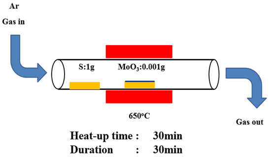
Figure 1.
Schematic of a growing MoS2 film.
MoS2 Transfer Process
A spin coater was used to coat uniformly the photoresistant PMMA A5 on the substrate to transfer MoS2 after CVD growth on the Cu2O surface and left for the PMMA to dry. The substrate was covered with photoresistant liquid into 2 M NaOH as an etching solution for separating the substrate and PMMA A5. The removed photoresist was placed in DI water and blown dry with high-pressure nitrogen to prepare for the subsequent transfer. Then, PMMA A5 was placed on the original SiO2 substrate, which was cut to an appropriate size with a three-axis leveling table and placed on the surface of the Cu2O substrate. The temperature was set to 210° for about 30 s to make the PMMA adhere to the substrate. The sample was soaked in acetone for 30 min, and photoresistance was removed, leaving MoS2 to complete the entire transfer process (Figure 2).
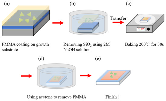
Figure 2.
MoS2 transfer flow chart: (a) PMMA coating on growth, (b) Removing SiO2 using 2M NaOH solution, (c) Baking 200 °C for 30s, (d) Remove PMMA by acetone, (e) Complete the entire transfer process.
3. Results
3.1. Growth Results of MoS2/Cu2O
Based on the above growth methods and measurement results, the CVD-grown MoS2 was transferred electrochemically to grown Cu2O (Supplementary Section S4 for the results of Cu2O electrochemical growth under different parameters). Material and optical characteristics were analyzed: Raman mapping (Supplementary Section S2.2 for micro-Raman Spectroscopy), SEM (Supplementary Section S2.5 for scanning electron microscope), and SHG measurements (Supplementary Section S2.8 for multiphoton excitation microscope).
3.1.1. Cu2O Flattening Comparison
This study has used the Cu2O film grown by the electrochemical method as the template for MoS2 transfer. The SEM image is used to detect the success rate of the transfer, and the result is consistent with the Cu2O image without transfer in the SEM image, as shown in Figure 3a,b. The reason for the failure is that the Cu2O surface used for the electrochemical method is quite rough, and the rough surface causes the MoS2 transfer to be broken or unable to be transferred because of the uneven surface. Afterward, the Cu2O film was ground to smoothen the Cu2O surface and facilitate the subsequent transfer of MoS2 while maintaining the integrity of the morphological characteristics of MoS2 and reducing the transfer failure rate. Figure 4a shows the AFM data results of Cu2O before grinding. Under the following parameters, i.e., Z range of 740.16 nm, Rms of 97.496, and data scale of 0–800 nm (height), Figure 4b shows the results of Cu2O after surface polishing by grinding. Under the following parameters, i.e., Z range of 94.623 nm, Rms of 3.849 nm, and data scale of 0 50 nm (height), the top and flat views of the Cu2O film in the SEM image are shown in Figure 3c,d, respectively. The surface after grinding is smooth. According to the above data, grinding may be used to treat the Cu2O surface.
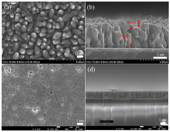
Figure 3.
(a) Represents the front view of the Cu2O film before polishing, (b) represent the side view of the Cu2O film before polishing, (c) show the SEM images of the top view after Cu2O polishing, (d) show the SEM images of the front view after Cu2O polishing.
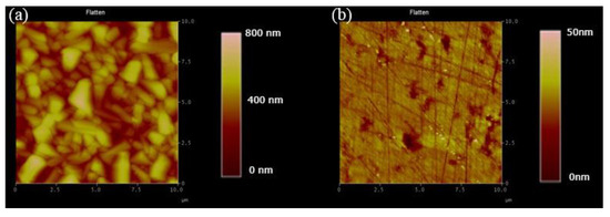
Figure 4.
(a,b) AFM measurements of the Cu2O film before and after polishing.
3.1.2. MoS2 Transfer Result on Cu2O
After the Cu2O surface is polished by the abovementioned grinding method, the SEM image result shows that the surface is smoother than the original unpolished surface, and the surface roughness is reduced by 96% in the AFM measurement result (Supplementary Section S2.6 for atomic force microscope). Then CVD-grown MoS2 film is transferred to the Cu2O surface, and SEM is performed (Figure 5). Although few irregularities are observed on the surface of the Cu2O, SEM analysis shows that MoS2 is transferred successfully, and the morphological characteristics of MoS2 are completely present on the surface of Cu2O.
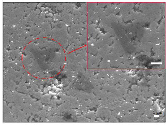
Figure 5.
SEM image of MoS2 transferred to the Cu2O surface.
3.1.3. Analysis of MoS2/Cu2O Materials and Optical Properties
After the transfer of the CVD-grown MoS2 film onto the electrochemically grown Cu2O surface. Its material and optical properties are analyzed by employing OM (Supplementary Section S2.4 for optical microscope), SHG images, SEM, and Raman and PL mapping. A multiphoton image is used to identify the signal display during the MoS2 transfer (Figure 6). The morphological characteristics of MoS2 grown by CVD are obvious. A core point exists in most triangles, and when this core point corresponds to a multiphoton image, the signal becomes stronger than the color of the triangles other than the core point. Figure 6b shows the multiphoton image of MoS2/Cu2O/ITO after the transfer. Although many blue irregularities in the image, they are not evenly dispersed to make it clear whether they are MoS2 triangles.
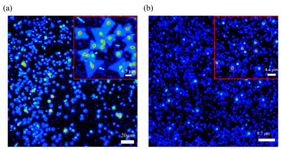
Figure 6.
Multiphoton images of (a) MoS2/SiO2/Si and of (b) MoS2/Cu2O/ITO.
However, the comparison of the obvious bright spots in the image in Figure 6a suggests that a bright spot signal may be the core image after MoS2 transfer and because Cu2O is not completely flat like the SiO2 surface after being polished. Moreover, this bright spot at the center of MoS2 is due to the nucleation of MoS2. The growth parameters, such as carrier gas, growth temperature, precursors, substrates, and promoters can affect the nucleation and growth modes of MoS2 [61]. However, Ho Kwon Kim et al. has shown that the pre-exposure of growth substrates to alkali metal halides and the Mo precursor before the growth stage appears can suppress nucleation of MoS2 [62]. Therefore, the other blue part may be a multi-photon image of a mixture of MoS2 and Cu2O. As shown in Figure 5, the grown MoS2 has been successfully transferred to the Cu2O film. These two data can be combined, proving that MoS2 has been successfully transferred to the Cu2O film by grinding and transfer. Raman mapping, which is the best method to analyze the number of layers, has been used to analyze the image of the transferred MoS2/Cu2O sample [63,64,65]. In this study, a 532 nm band is used as a laser excitation light source. From Figure 7b we can observe that the blue-green area is the MoS2 film, and the red area is part of a Cu2O film. The 532 nm band was used as the laser excitation light source in this study. As shown in Figure 7a, the Raman shift of MoS2 has a peak at 384.3 before transfer while the Raman shift had a peak at 402.8 cm−1 after the transfer. The Raman shift of Cu2O before the transfer has a peak at 221.8 cm−1. After transferring MoS2 onto the Cu2O film, the Raman shift did reach peaks at 221.8, 384.3, and 402.8 cm−1. It can be clearly inferred that the Raman peak of Cu2O appearing at 221.8 cm−1 indicates that the surface of Cu2O was partially oxidized. Similarly, the Raman shifts of MoS2 at 384.3 and 402.8 cm−1 are in accordance with E12g and A1g, respectively, and combined vibrations of two different phonons (A1g(M)−LA(M)), respectively, which indicates the existence of MoS2 structures [66,67,68,69]. In the Cu2O/MoS2 composite films, the diffraction peaks of Cu2O and MoS2 are still observed. The result shows that the grown MoS2 has a uniform film in the image and can replace the morphology. E12g and A1g vibration modes are the main signals for the judgment of MoS2. The two vibration modes are highly dependent on the thickness of MoS2. When the Δk value of the subtraction of E12g and A1g peaks is less than 20 cm−1, the analyzed MoS2 is regarded as a single-layer structure.
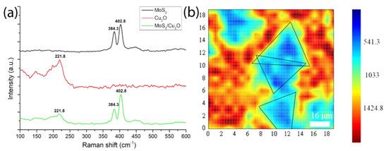
Figure 7.
(a) Raman spectrum after MoS2 transfer to Cu2O surface and (b) Raman mapping of MoS2/Cu2O.
Figure 8a shows the OM image of MoS2/Cu2O, Figure 8b illustrates the 625-band image selected for the PL mapping image. The MoS2 spectrum consists of two peaks corresponding to the A1 and B1 excitons at 667 nm (1.86 eV) and 627 nm (1.97 eV), respectively. The measured PL for Cu2O grown by the electrochemical method was about 720–900 nm. In the measurement of the PN heterostructure material combination of MoS2/Cu2O, Raman measurement was first performed on the OM image. After the signal of MoS2 is found, PL measurement is carried out, and the combined structure is examined through the measurement results to show that the band range covers 625–900 nm. We found that a micro signal is generated at about 627 nm in the orange elliptical dashed circle, and the wavelength of 627 nm belongs to the B2 excitons of MoS2. The signal gradually increases when it approaches 670 nm. However, the Cu2O signal is not in this part because its light-emitting band starts to generate signals from 720 nm. Therefore, the Cu2O film may be too thick, and the single-layer MoS2 film thickness is only 0.7 nm, so the two heterostructure materials are combined in the wavelength range of 670–700 nm. The entire signal undergoes a red-shifted phenomenon because the Cu2O film signal is strong.
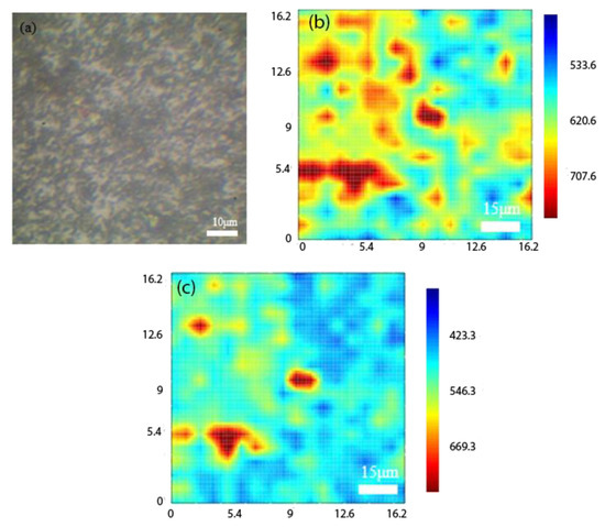
Figure 8.
(a) OM image of MoS2/Cu2O, (b) 625 band for PL mapping image, (c) 675 band for PL mapping image.
3.2. Photocurrent Response Analysis
This research uses the preparation of biosensors, and the photocurrent measurement system and impedance analysis system set up in the laboratory (see Supplement 1, Section S6 for Analysis of Structural Characteristics of Photoelectrochemical Biosensors). The photocurrent measurement of the three lung cancer cells A549, H460 and H520 was carried out by the carrier transport mechanism of photogenerated charge, and the zigzags-toothed microelectrode was used to perform aggregation and impedance analysis of the cancer cells. In this study, we utilized two characteristic substances, glutathione (GSH) and glutathione disulfide (GSSG), to verify the detection mechanism of the developed biosensor. Generally, GSH in cells exists in two forms: 90% of GSH is present in the cytoplasm as reduced GSH, and 10% is present in the mitochondria. For healthy cells, the ratio of GSH to GSSG is greater than 10:1. However, when cells become cancerous, the ratio of GSH to GSSG decreases [70,71]. Because the majority carriers in N-type PEC are electrons and hence GSSG participating in PEC reaction is more significant. When irradiated, electron-hole pairs are generated, GSSG recombines with photo-generated electrons, and photo-generated holes are detected, forming a system of hole currents. As the degree of canceration becomes more severe, the concentration of GSSG contained in cancer cells increases, and the measured photocurrent also increases [72,73]. On the contrary, the majority of carriers in the P-type PEC biosensor are holes and hence GSH participates in the PEC reaction more significantly. After being illuminated, GSH recombines with photo-generated holes, photo-generated electrons are detected, and a system of electron flow is formed. The more severe the carcinogenesis of the structure, the smaller the GSH concentration and also a decrease of the photocurrent [74,75]. As shown in Figure 9 the photocurrent decreased with the increase of suspended cell density, which indicated that more GSH was involved in the PEC process. From Figure 10, it can be known that different cells have different amounts of change, there is a highly linear relationship between the photocurrent change and the number of cells, and the linear regression of the three cell types is as high as 99%. The slopes corresponding to the three cell lines A549, NCI-H460 and NCI-H520 were approximately 0.000452, 0.000749 and 0.000174, respectively. By measuring the magnitude of the photocurrent, we can calculate the regression curve equation, thereby identifying which cell of the three cells is. In the growth mechanism of Cu2O, as the thickness increases, the stress or dislocation will increase, resulting in a certain optimal thickness of the material. Previous studies also shows that the best growth thickness of Cu2O under the environment and parameters of our growth is 2 μm [76].
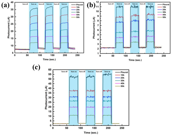
Figure 9.
P. (a) Photocurrent responses of A549 under different cell numbers, (b) Photocurrent responses of NCI-H460 under different cell numbers and (c) Photocurrent responses of NCI-H520 under different cell numbers.
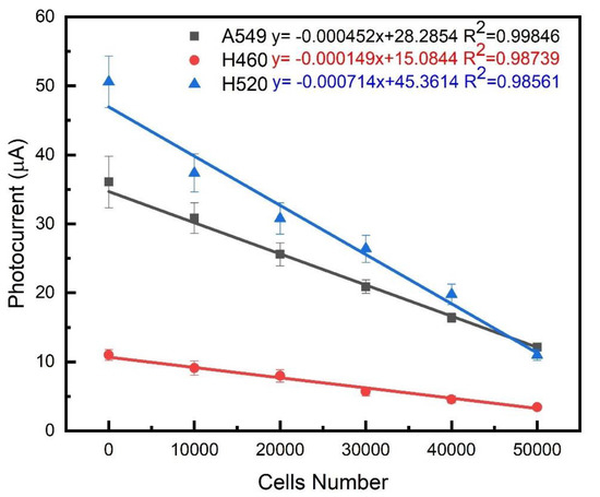
Figure 10.
Linear relationship between photocurrent changes and cell number in three lung cancer cell lines on biosensing chips.
4. Discussion
When the MoS2 film has a single-layer structure, the A1g signal is stronger than that of a multilayer film. If the MoS2 film has a multilayer structure, the E12g signal is stronger than that of a single-layer film. The PL signal of MoS2 also decreases as the number of layers increases. Therefore, we can observe the contrast of the image by selecting the PL mapping images of 625 and 675 nm, corresponding to the color bar value. Single- and multi-layer MoS2 film signals are found in the selected 625-band image compared with much fewer signals in the 675-band image. When we grow the MoS2 film, single- and multi-layer structures form. In the selection of images for mapping, more multi-layer MoS2 films are covered. The PL measurement results in this study use a 532 nm laser as the excitation light source to measure the PL of a single-layer MoS2 film. The measurement results show that a strong signal is generated at the wavelength of 667 nm, and the energy is 1.84 eV after conversion. It is the energy gap of single-layer MoS2. However, from Gang Li et al., the energy band alignment of bulk MoS2 and single layer MoS2 was observed at 1.4 eV and 1.78 eV, respectively [29]. From our study, the single layer MoS2 was observed at 1.84 eV, close to the previous observations. The future scope of this project can be split into two aspects. First, after the two materials are combined, by using them as electric double-layer transistors their electrical properties can be tested. After confirming the positive state of the oxide trap. We can also try to bombard the element with high-energy particles to explore its characteristic influence and figure out if it affects the transformation of the mechanism. If the result of the electron beam bombardment affects the element and causes the characteristics to change, it can be checked again whether the electrical property changes from the positive oxide trap state to the negative interface trap state. Second, CVD can be performed to grow MoS2 in the 2H phase. MoS2 has three crystal structures: 2H (semiconductor characteristics), 1T (metallic characteristics), and 3R (semiconductor characteristics). The intensity difference can be detected in the PL mapping and electrostatic force microscope (EFM) images of 2H-MoS2 and 1T-MoS2. The future scope of this study is to collect a large amount of data to build a large-scale database by measuring the cell impedance and photocurrent in the patient’s pleural effusion. After analyzing the data through Artificial Intelligence (AI), a human-machine display interface will be designed which provides the types of cancer cells defined by the system, assisting physicians to determine the patient’s cancer status and provide appropriate treatment methods.
5. Conclusions
In this study, an electrochemical method was used to grow a Cu2O film with a uniform and superior crystal lattice. The micro-roughened surface structure of Cu2O was polished by grinding. Then, CVD-grown single crystal MoS2 was transferred to the Cu2O film. OM, SHG, SEM, Raman, and PL mapping measurements were used to analyze the combination of the two materials. Electrochemical methods were successfully used to achieve relatively good electrical properties. TEM showed that Cu2O is a single crystal structure, and SEM revealed that the surface should be processed by subsequent grinding methods. After grinding and polishing were performed, AFM and SEM were used to obtain the experimental results. MoS2 structure was grown through CVD, and E12g and A1g peaks were obtained via Raman analysis. The main luminescence peak at 667 nm was determined through PL analysis. The single layer of MoS2 was transferred to the polished Cu2O surface, which was confirmed by SEM and SHG results. Raman and PL mapping image analysis on MoS2/Cu2O indicated that the grown MoS2 had a uniform film. The combined structure was measured through PL measurement to verify that the band range covered 625–900 nm. A micro signal was found at the 627 nm wavelength. It belonged to the B2 excitons of MoS2 and tended to increase gradually as it approached 670 nm. The Cu2O film was too thick, whereas the thickness of the single-layer MoS2 film was only 0.7 nm. As such, the two heterostructure materials combined in the wavelength range of 670–700 nm. The strong signal of the Cu2O film itself led to a red shift in the entire signal. This study also successfully fabricated a low-cost PEC biosensor that is highly sensitive to lung cancer cells which is a rapid way to detect lung cancer cell types in hydroplegia. The photocurrent response is measured using the MoS2/Cu2O biochip material grown by electrochemical deposition. As the number of cancer cells measured increases, the content of oxidized GSSG also increases, and the measured photocurrent decreases accordingly. It is also possible to use dielectrophoresis to gather cancer cells to form a pearl string, measure unlabeled cancer cells, and use the slope of the admittance value to shape lung cancer cells. The linear regression curve is compared with the admittance value and the photocurrent measurement value to distinguish the types of cancer cells in the pleural effusion.
Supplementary Materials
The following supporting information can be downloaded at: https://www.mdpi.com/article/10.3390/ijms23094745/s1.
Author Contributions
Conceptualization, V.E.F., S.-W.F. and. S.B.A.; methodology, S.-W.F., Y.-M.T., Y.-C.H. and Y.-S.L.; software, S.-W.F., V.E.F. and Y.-S.L.; validation, S.B.A., S.-W.F. and H.-C.W.; formal analysis, S.-W.F., Y.-M.T. and Y.-S.L.; investigation, Y.-S.L., Y.-H.W. and A.M.; resources, S.-W.F., Y.-M.T., Y.-C.H. and Y.-H.W.; data curation, S.B.A.; writing–original draft preparation, S.B.A., A.M. and Y.-H.W.; writing–review and editing, A.M. and H.-C.W.; supervision, S.-W.F., V.E.F. and H.-C.W.; and project administration, H.-C.W. All authors have read and agreed to the published version of the manuscript.
Funding
This research was supported by the Ministry of Science and Technology, The Republic of China under the grants MOST 105-2923-E-194-003 MY3, 108-2823-8-194-002, 109-2622-8-194-001-TE1, and 109-2622-8-194-007. This work was financially/partially supported by the Advanced Institute of Manufacturing with High-tech Innovations (AIM-HI) and the Center for Innovative Research on Aging Society (CIRAS) from The Featured Areas Research Center Program within the framework of the Higher Education Sprout Project by the Ministry of Education (MOE) and Kaohsiung Armed Forces General Hospital research project 108-016 in Taiwan.
Institutional Review Board Statement
Not Applicable.
Informed Consent Statement
Not Applicable.
Data Availability Statement
Not Applicable.
Conflicts of Interest
The authors declare no conflict of interest.
References
- Geim, A.K.; Novoselov, K.S. The rise of graphene. In Nanoscience and Technology: A Collection of Reviews from Nature Journals; World Scientific: Singapore, 2010; pp. 11–19. [Google Scholar]
- Sarma, S.D.; Adam, S.; Hwang, E.H.; Rossi, E. Electronic transport in two-dimensional graphene. Rev. Mod. Phys. 2011, 83, 407. [Google Scholar] [CrossRef] [Green Version]
- Lin, X.; Su, L.; Si, Z.; Zhang, Y.; Bournel, A.; Zhang, Y.; Klein, J.-O.; Fert, A.; Zhao, W. Gate-Driven Pure Spin Current in Graphene. Phys. Rev. Appl. 2017, 8, 034006. [Google Scholar] [CrossRef]
- Wu, C.; Zhang, J.; Tong, X.; Yu, P.; Xu, J.; Wu, J.; Wang, Z.M.; Lou, J.; Chueh, Y.-L. A critical review on enhancement of photocatalytic hydrogen production by molybdenum disulfide: From growth to interfacial activities. Small 2019, 15, 1900578. [Google Scholar] [CrossRef] [PubMed]
- Yang, D.; Wang, H.; Luo, S.; Wang, C.; Zhang, S.; Guo, S. Paper-Cut Flexible Multifunctional Electronics Using MoS2 Nanosheet. Nanomaterials 2019, 9, 922. [Google Scholar] [CrossRef] [PubMed] [Green Version]
- Zhang, Y.; Wan, Q.; Yang, N. Recent Advances of Porous Graphene: Synthesis, Functionalization, and Electrochemical Applications. Small 2019, 15, e1903780. [Google Scholar] [CrossRef] [PubMed]
- Choi, M.S.; Lee, G.-H.; Yu, Y.-J.; Lee, D.-Y.; Lee, S.H.; Kim, P.; Hone, J.; Yoo, W.J. Controlled charge trapping by molybdenum disulphide and graphene in ultrathin heterostructured memory devices. Nat. Commun. 2013, 4, 1624. [Google Scholar] [CrossRef] [PubMed]
- Han, T.; Liu, H.; Wang, S.; Chen, S.; Xie, H.; Yang, K. Probing the Field-Effect Transistor with Monolayer MoS2 Prepared by APCVD. Nanomaterials 2019, 9, 1209. [Google Scholar] [CrossRef] [PubMed] [Green Version]
- Lee, C.-H.; Lee, G.-H.; van der Zande, A.M.; Chen, W.; Li, Y.; Han, M.; Cui, X.; Arefe, G.; Nuckolls, C.; Heinz, T.F.; et al. Atomically thin p–n junctions with van der Waals heterointerfaces. Nat. Nanotechnol. 2014, 9, 676–681. [Google Scholar] [CrossRef] [Green Version]
- Lu, G.Z.; Wu, M.-J.; Lin, T.-N.; Chang, C.-Y.; Lin, W.-L.; Chen, Y.T.; Hou, C.-F.; Cheng, H.-J.; Lin, T.-Y.; Shen, J.-L.; et al. Electrically Pumped White-Light-Emitting Diodes Based on Histidine-Doped MoS2 Quantum Dots. Small 2019, 15, 1901908. [Google Scholar] [CrossRef]
- Park, Y.J.; Sharma, B.K.; Shinde, S.M.; Kim, M.-S.; Jang, B.; Kim, J.-H.; Ahn, J.-H. All MoS2-Based Large Area, Skin-Attachable Active-Matrix Tactile Sensor. ACS Nano 2019, 13, 3023–3030. [Google Scholar] [CrossRef]
- Radisavljevic, B.; Radenovic, A.; Brivio, J.; Giacometti, V.; Kis, A. Single-layer MoS2 transistors. Nat. Nanotechnol. 2011, 6, 147–150. [Google Scholar] [CrossRef]
- Roh, J.; Ryu, J.H.; Baek, G.W.; Jung, H.; Seo, S.G.; An, K.; Jeong, B.G.; Lee, D.C.; Hong, B.H.; Bae, W.K.; et al. Threshold Voltage Control of Multilayered MoS2 Field-Effect Transistors via Octadecyltrichlorosilane and their Applications to Active Matrixed Quantum Dot Displays Driven by Enhancement-Mode Logic Gates. Small 2019, 15, 1803852. [Google Scholar] [CrossRef] [PubMed]
- Zhao, J.; Li, N.; Yu, H.; Wei, Z.; Liao, M.; Chen, P.; Wang, S.; Shi, D.; Sun, Q.; Zhang, G. Highly Sensitive MoS2 Humidity Sensors Array for Noncontact Sensation. Adv. Mater. 2017, 29. [Google Scholar] [CrossRef] [PubMed]
- Zhang, P.; Yang, S.; Pineda-Gómez, R.; Ibarlucea, B.; Ma, J.; Lohe, M.R.; Akbar, T.F.; Baraban, L.; Cuniberti, G.; Feng, X.; et al. Electrochemically Exfoliated High-Quality 2H-MoS2 for Multiflake Thin Film Flexible Biosensors. Small 2019, 15, 1901265. [Google Scholar] [CrossRef]
- Yang, K.; Liu, H.; Wang, S.; Li, W.; Han, T. A Horizontal-Gate Monolayer MoS2 Transistor Based on Image Force Barrier Reduction. Nanomaterials 2019, 9, 1245. [Google Scholar] [CrossRef] [PubMed] [Green Version]
- Yadav, V.; Roy, S.; Singh, P.; Khan, Z.; Jaiswal, A. 2D MoS2-based nanomaterials for therapeutic, bioimaging, and biosensing applications. Small 2019, 15, 1803706. [Google Scholar] [CrossRef] [PubMed] [Green Version]
- Shin, M.; Yoon, J.; Yi, C.; Lee, T.; Choi, J.-W. Flexible HIV-1 Biosensor Based on the Au/MoS2 Nanoparticles/Au Nanolayer on the PET Substrate. Nanomaterials 2019, 9, 1076. [Google Scholar] [CrossRef] [PubMed] [Green Version]
- Sarkar, D.; Liu, W.; Xie, X.; Anselmo, A.C.; Mitragotri, S.; Banerjee, K. MoS2 Field-Effect Transistor for Next-Generation Label-Free Biosensors. ACS Nano 2014, 8, 3992–4003. [Google Scholar] [CrossRef]
- Jia, X.; Huang, J.; Li, Y.; Yang, J.; Song, H. Monodisperse Cu nanoparticles @ MoS2 nanosheets as a lubricant additive for improved tribological properties. Appl. Surf. Sci. 2019, 494, 430–439. [Google Scholar] [CrossRef]
- Zhao, Y.-F.; Yang, Z.-Y.; Zhang, Y.-X.; Jing, L.; Guo, X.; Ke, Z.; Hu, P.; Wang, G.; Yan, Y.-M.; Sun, K.-N. Cu2O Decorated with Cocatalyst MoS2 for Solar Hydrogen Production with Enhanced Efficiency under Visible Light. J. Phys. Chem. C 2014, 118, 14238–14245. [Google Scholar] [CrossRef]
- Paracchino, A.; Laporte, V.; Sivula, K.; Grätzel, M.; Thimsen, E. Highly active oxide photocathode for photoelectrochemical water reduction. Nat. Mater. 2011, 10, 456–461. [Google Scholar] [CrossRef]
- Mahmoud, M.A.; Qian, W.; El-Sayed, M.A. Following Charge Separation on the Nanoscale in Cu2O–Au Nanoframe Hollow Nanoparticles. Nano Lett. 2011, 11, 3285–3289. [Google Scholar] [CrossRef]
- Radi, A.; Pradhan, D.; Sohn, Y.; Leung, K.T. Nanoscale shape and size control of cubic, cuboctahedral, and octahedral Cu−Cu2O core−shell nanoparticles on Si (100) by one-step, templateless, capping-agent-free electrodeposition. ACS Nano 2010, 4, 1553–1560. [Google Scholar] [CrossRef]
- De Jongh, P.E.; Vanmaekelbergh, D.; Kelly, J.J. Photoelectrochemistry of Electrodeposited Cu2O. J. Electrochem. Soc. 2000, 147, 486–489. [Google Scholar] [CrossRef]
- Li, Z.; Ezhilarasu, G.; Chatzakis, I.; Dhall, R.; Chen, C.-C.; Cronin, S.B. Indirect Band Gap Emission by Hot Electron Injection in Metal/MoS2 and Metal/WSe2 Heterojunctions. Nano Lett. 2015, 15, 3977–3982. [Google Scholar] [CrossRef]
- Zhao, X.; Li, Y.; Guo, Y.; Chen, Y.; Su, Z.; Zhang, P. Coral-like MoS2/Cu2O porous nanohybrid with dual-electrocatalyst performances. Adv. Mater. Interfaces 2016, 3, 1600658. [Google Scholar] [CrossRef]
- Mukundan, A.; Tsao, Y.-M.; Artemkina, S.B.; Fedorov, V.E.; Wang, H.-C. Growth Mechanism of Periodic-Structured MoS2 by Transmission Electron Microscopy. Nanomaterials 2021, 12, 135. [Google Scholar] [CrossRef]
- Fang, L.; Wang, F.; Chen, Z.; Qiu, Y.; Zhai, T.; Hu, M.; Zhang, C.; Huang, K. Flower-like MoS2 decorated with Cu2O nanoparticles for non-enzymatic amperometric sensing of glucose. Talanta 2017, 167, 593–599. [Google Scholar] [CrossRef]
- Li, G.; Zhang, W.; Hou, J.; Li, T.; Li, P.; Wang, Y.; Liu, J.; Wang, K. Enhanced visible light photochemical activity and stability of MoS2/Cu2O nanocomposites by tunable heterojunction. Mater. Today Commun. 2020, 23, 100933. [Google Scholar] [CrossRef]
- Koyun, O.; Sahin, Y. Voltammetric determination of nitrite with gold nanoparticles/poly (methylene blue)-modified pencil graphite electrode: Application in food and water samples. Ionics 2018, 24, 3187–3197. [Google Scholar] [CrossRef]
- Amini, N.; Gholivand, M.B.; Shamsipur, M.; Movahedi, A.A.M.; Farahi, S.; Habibi-Rezaei, M.; Maleki, A.; Rezaee, M.; Naderi, K. Fabrication of a glycation induced amyloid nanofibril and polyalizarin yellow R nanobiocomposite: Application for electrocatalytic determination of hydrogen peroxide. Int. J. Biol. Macromol. 2018, 123, 1297–1304. [Google Scholar] [CrossRef] [PubMed]
- Agrisuelas, J.; González-Sánchez, M.-I.; Gómez-Monedero, B.; Valero, E. A Comparative Study of Poly(Azure A) Film-Modified Disposable Electrodes for Electrocatalytic Oxidation of H2O2: Effect of Doping Anion. Polymers 2018, 10, 48. [Google Scholar] [CrossRef] [PubMed] [Green Version]
- Liu, Y.; Song, N.; Ma, Z.; Zhou, K.; Gan, Z.; Gao, Y.; Tang, S.; Chen, C. Synthesis of a poly (N-methylthionine)/reduced graphene oxide nanocomposite for the detection of hydroquinone. Mater. Chem. Phys. 2019, 223, 548–556. [Google Scholar] [CrossRef]
- da Silva, W.; Ghica, M.E.; Brett, C.M. Novel nanocomposite film modified electrode based on poly (brilliant cresyl blue)-deep eutectic solvent/carbon nanotubes and its biosensing applications. Electrochim. Acta 2019, 317, 766–777. [Google Scholar] [CrossRef]
- Shamspur, T.; Biniaz, Z.; Mostafavi, A.; Torkzadeh-Mahani, M.; Mohamadi, M. An Electrochemical Immunosensor Based on Poly(Thionine)-Modified Carbon Paste Electrode for the Determination of Prostate Specific Antigen. IEEE Sens. J. 2018, 18, 4861–4868. [Google Scholar] [CrossRef]
- Ali, S.; Gupta, A.; Shafiei, M.; Langford, S. Recent Advances in Perylene Diimide-Based Active Materials in Electrical Mode Gas Sensing. Chemosensors 2021, 9, 30. [Google Scholar] [CrossRef]
- Kozitsina, A.N.; Svalova, T.S.; Malysheva, N.N.; Okhokhonin, A.V.; Vidrevich, M.B.; Brainina, K.Z. Sensors Based on Bio and Biomimetic Receptors in Medical Diagnostic, Environment, and Food Analysis. Biosensors 2018, 8, 35. [Google Scholar] [CrossRef] [Green Version]
- Feng, T.; Chen, X.; Qiao, X.; Sun, Z.; Wang, H.; Qi, Y.; Hong, C. Graphene oxide supported rhombic dodecahedral Cu2O nanocrystals for the detection of carcinoembryonic antigen. Anal. Biochem. 2015, 494, 101–107. [Google Scholar] [CrossRef]
- Ma, H.; Li, Y.; Wang, Y.; Hu, L.; Zhang, Y.; Fan, D.; Yan, T.; Wei, Q. Cubic Cu2O nanoframes with a unique edge-truncated structure and a good electrocatalytic activity for immunosensor application. Biosens. Bioelectron. 2016, 78, 167–173. [Google Scholar] [CrossRef]
- Park, J.C.; Kim, J.; Kwon, H.; Song, H. Gram-Scale Synthesis of Cu2O Nanocubes and Subsequent Oxidation to CuO Hollow Nanostructures for Lithium-Ion Battery Anode Materials. Adv. Mater. 2009, 21, 803–807. [Google Scholar] [CrossRef]
- Wang, H.; Zhang, Y.; Wang, Y.; Ma, H.; Du, B.; Wei, Q. Facile synthesis of cuprous oxide nanowires decorated graphene oxide nanosheets nanocomposites and its application in label-free electrochemical immunosensor. Biosens. Bioelectron. 2017, 87, 745–751. [Google Scholar] [CrossRef]
- Su, S.; Sun, H.; Cao, W.; Chao, J.; Peng, H.; Zuo, X.; Yuwen, L.; Fan, C.; Wang, L. Dual-Target Electrochemical Biosensing Based on DNA Structural Switching on Gold Nanoparticle-Decorated MoS2 Nanosheets. ACS Appl. Mater. Interfaces 2016, 8, 6826–6833. [Google Scholar] [CrossRef]
- Su, S.; Zou, M.; Zhao, H.; Yuan, C.; Xu, Y.; Zhang, C.; Wang, L.; Fan, C.; Wang, L. Shape-controlled gold nanoparticles supported on MoS2 nanosheets: Synergistic effect of thionine and MoS2 and their application for electrochemical label-free immunosensing. Nanoscale 2015, 7, 19129–19135. [Google Scholar] [CrossRef]
- Wang, X.; Shen, L.; Deng, W.; Yan, M.; Liu, H.; Ge, S.; Yu, J.; Song, X. A sensitive electrochemiluminescent immunosensor based on 3D-flower-like MoS2 microspheres and using AuPt nanoparticles for signal amplification. RSC Adv. 2016, 6, 23411–23419. [Google Scholar] [CrossRef]
- Wu, I.-C.; Weng, Y.-H.; Lu, M.-Y.; Jen, C.-P.; Fedorov, V.E.; Chen, W.C.; Wu, M.T.; Kuo, C.-T.; Wang, H.-C. Nano-structure ZnO/Cu2O photoelectrochemical and self-powered biosensor for esophageal cancer cell detection. Opt. Express 2017, 25, 7689–7706. [Google Scholar] [CrossRef]
- Chen, Y.-S.; Liao, C.-H.; Chueh, Y.-L.; Lai, C.-C.; Chen, L.-Y.; Chu, A.-K.; Kuo, C.-T.; Wang, H.-C. High performance Cu2O/ZnO core-shell nanorod arrays synthesized using a nanoimprint GaN template by the hydrothermal growth technique. Opt. Mater. Express 2014, 4, 1473–1486. [Google Scholar] [CrossRef]
- Zhao, Y.; Luo, X.; Li, H.; Zhang, J. Interlayer breathing and shear modes in few-trilayer MoS2 and WSe2. Nano Lett. 2013, 13, 1007–1015. [Google Scholar] [CrossRef] [Green Version]
- Li, H.; Wu, J.; Yin, Z.; Zhang, H. Preparation and Applications of Mechanically Exfoliated Single-Layer and Multilayer MoS2 and WSe2 Nanosheets. Acc. Chem. Res. 2014, 47, 1067–1075. [Google Scholar] [CrossRef]
- Li, H.; Lu, G.; Yin, Z.; He, Q.; Li, H.; Zhang, Q.; Zhang, H. Optical identification of single-and few-layer MoS2 sheets. Small 2012, 8, 682–686. [Google Scholar] [CrossRef]
- Li, K.-C.; Lu, M.-Y.; Nguyen, H.T.; Feng, S.-W.; Artemkina, S.B.; Fedorov, V.E.; Wang, H.-C. Intelligent Identification of MoS2 Nanostructures with Hyperspectral Imaging by 3D-CNN. Nanomaterials 2020, 10, 1161. [Google Scholar] [CrossRef]
- Wang, Q.; Lei, Y.; Wang, Y.; Liu, Y.; Song, C.; Zeng, J.; Song, Y.; Duan, X.; Wang, D.; Li, Y. Atomic-scale engineering of chemical-vapor-deposition-grown 2D transition metal dichalcogenides for electrocatalysis. Energy Environ. Sci. 2020, 13, 1593–1616. [Google Scholar] [CrossRef]
- Cai, Z.; Liu, B.; Zou, X.; Cheng, H.-M. Chemical Vapor Deposition Growth and Applications of Two-Dimensional Materials and Their Heterostructures. Chem. Rev. 2018, 118, 6091–6133. [Google Scholar] [CrossRef] [PubMed]
- Jeon, J.; Jang, S.K.; Jeon, S.M.; Yoo, G.; Jang, Y.H.; Park, J.-H.; Lee, S. Layer-controlled CVD growth of large-area two-dimensional MoS2 films. Nanoscale 2014, 7, 1688–1695. [Google Scholar] [CrossRef] [PubMed]
- Lee, Y.-H.; Zhang, X.-Q.; Zhang, W.; Chang, M.-T.; Lin, C.-T.; Chang, K.-D.; Yu, Y.-C.; Wang, J.T.-W.; Chang, C.-S.; Li, L.-J.; et al. Synthesis of Large-Area MoS2 Atomic Layers with Chemical Vapor Deposition. Adv. Mater. 2012, 24, 2320–2325. [Google Scholar] [CrossRef] [Green Version]
- van der Zande, A.M.; Huang, P.Y.; Chenet, D.A.; Berkelbach, T.C.; You, Y.; Lee, G.-H.; Heinz, T.F.; Reichman, D.R.; Muller, D.A.; Hone, J.C. Grains and grain boundaries in highly crystalline monolayer molybdenum disulphide. Nat. Mater. 2013, 12, 554–561. [Google Scholar] [CrossRef] [Green Version]
- Najmaei, S.; Liu, Z.; Zhou, W.; Zou, X.; Shi, G.; Lei, S.; Yakobson, B.I.; Idrobo, J.C.; Ajayan, P.M.; Lou, J. Vapour phase growth and grain boundary structure of molybdenum disulphide atomic layers. Nat. Mater. 2013, 12, 754–759. [Google Scholar] [CrossRef]
- Hyun, C.-M.; Choi, J.-H.; Lee, S.W.; Park, J.H.; Lee, K.-T.; Ahn, J.-H. Synthesis mechanism of MoS2 layered crystals by chemical vapor deposition using MoO3 and sulfur powders. J. Alloy. Compd. 2018, 765, 380–384. [Google Scholar] [CrossRef]
- Liu, H.; Bin Yang, R.; Yang, W.; Jin, Y.; Lee, C.J. Atomic layer deposition and post-growth thermal annealing of ultrathin MoO3 layers on silicon substrates: Formation of surface nanostructures. Appl. Surf. Sci. 2018, 439, 583–588. [Google Scholar] [CrossRef]
- Pondick, J.V.; Woods, J.M.; Xing, J.; Zhou, Y.; Cha, J.J. Stepwise sulfurization from MoO3 to MoS2 via chemical vapor deposition. ACS Appl. Nano Mater. 2018, 1, 5655–5661. [Google Scholar] [CrossRef]
- Kim, H.; Ovchinnikov, D.; Deiana, D.; Unuchek, D.; Kis, A. Suppressing Nucleation in Metal–Organic Chemical Vapor Deposition of MoS2 Monolayers by Alkali Metal Halides. Nano Lett. 2017, 17, 5056–5063. [Google Scholar] [CrossRef] [Green Version]
- Zhou, D.; Shu, H.; Hu, C.; Jiang, L.; Liang, P.; Chen, X. Unveiling the Growth Mechanism of MoS2 with Chemical Vapor Deposition: From Two-Dimensional Planar Nucleation to Self-Seeding Nucleation. Cryst. Growth Des. 2018, 18, 1012–1019. [Google Scholar] [CrossRef]
- KaiáLee, M. Large-area few-layered graphene film determination by multispectral imaging microscopy. Nanoscale 2015, 7, 9033–9039. [Google Scholar]
- Lu, M.-Y.; Wu, S.-C.; Wang, H.-C. Time-evolution of the electrical characteristics of MoS2 field-effect transistors after electron beam irradiation. Phys. Chem. Chem. Phys. 2018, 20, 9038–9044. [Google Scholar] [CrossRef]
- Hsieh, Y.-P.; Wang, Y.-W.; Ting, C.-C.; Wang, H.-C.; Chen, K.-Y.; Yang, C.-C. Effect of Catalyst Morphology on the Quality of CVD Grown Graphene. J. Nanomater. 2013, 2013, 1–6. [Google Scholar] [CrossRef] [Green Version]
- Park, B.; Lee, D.; Kim, H.-S.; Cho, Y.; Park, S.; Kim, C.; Lee, T.; Woo, D.H.; Kim, J.H. Synergetic enhancement in optical nonlinearity of Au nanoparticle decorated MoS2 via interaction between excitonic and surface plasmon resonances. Appl. Surf. Sci. 2020, 532, 147486. [Google Scholar] [CrossRef]
- Zhang, G.; Zhang, Z.; Xia, D.; Qu, Y.; Wang, W. Solar driven self−sustainable photoelectrochemical bacteria inactivation in scale−up reactor utilizing large−scale fabricable Ti/MoS2/MoOx photoanode. J. Hazard. Mater. 2020, 392, 122292. [Google Scholar] [CrossRef]
- Yuan, Y.; Wang, W.; Shi, Y.; Song, L.; Ma, C.; Hu, Y. The influence of highly dispersed Cu2O-anchored MoS2 hybrids on reducing smoke toxicity and fire hazards for rigid polyurethane foam. J. Hazard. Mater. 2019, 382, 121028. [Google Scholar] [CrossRef]
- Lu, C.; Xuan, H.; Zhou, Y.; Xu, X.; Zhao, Q.; Bai, J. Saturable and reverse saturable absorption in molybdenum disulfide dispersion and film by defect engineering. Photonics Res. 2020, 8, 1512. [Google Scholar] [CrossRef]
- Hao, X.-Y.; Bergh, J.; Brodin, O.; Heltman, U.; Mannervik, B. Acquired resistance to cisplatin and doxorubicin in a small cell lung cancer cell line is correlated to elevated expression of glutathione-linked detoxification enzymes. Carcinogenesis 1994, 15, 1167–1173. [Google Scholar] [CrossRef]
- Hammond, C.L.; Lee, T.K.; Ballatori, N. Novel roles for glutathione in gene expression, cell death, and membrane transport of organic solutes. J. Hepatol. 2001, 34, 946–954. [Google Scholar] [CrossRef]
- Kang, Z.; Yan, X.; Wang, Y.; Bai, Z.; Liu, Y.; Zhang, Z.; Lin, P.; Zhang, X.; Yuan, H.; Zhang, X.; et al. Electronic Structure Engineering of Cu2O Film/ZnO Nanorods Array All-Oxide p-n Heterostructure for Enhanced Photoelectrochemical Property and Self-powered Biosensing Application. Sci. Rep. 2015, 5, srep07882. [Google Scholar] [CrossRef] [PubMed] [Green Version]
- Tang, J.; Kong, B.; Wang, Y.; Xu, M.; Wang, Y.; Wu, H.; Zheng, G. Photoelectrochemical detection of glutathione by IrO2–Hemin–TiO2 nanowire arrays. Nano Lett. 2013, 13, 5350–5354. [Google Scholar] [CrossRef]
- Zang, Y.; Ju, Y.; Jiang, J.; Xu, Q.; Chu, M.; Xue, H. Cu2+-Modulated in situ growth of quantum dots for split-type photoelectrochemical immunoassay of prostate-specific antigen. Anal. 2019, 144, 4661–4666. [Google Scholar] [CrossRef]
- Zhu, Y.; Xu, Z.; Yan, K.; Zhao, H.; Zhang, J. One-Step Synthesis of CuO–Cu2O Heterojunction by Flame Spray Pyrolysis for Cathodic Photoelectrochemical Sensing of l-Cysteine. ACS Appl. Mater. Interfaces 2017, 9, 40452–40460. [Google Scholar] [CrossRef] [PubMed]
- Tran, M.H.; Cho, J.Y.; Sinha, S.; Gil Gang, M.; Heo, J. Cu2O/ZnO heterojunction thin-film solar cells: The effect of electrodeposition condition and thickness of Cu2O. Thin Solid Film. 2018, 661, 132–136. [Google Scholar] [CrossRef]
Publisher’s Note: MDPI stays neutral with regard to jurisdictional claims in published maps and institutional affiliations. |
© 2022 by the authors. Licensee MDPI, Basel, Switzerland. This article is an open access article distributed under the terms and conditions of the Creative Commons Attribution (CC BY) license (https://creativecommons.org/licenses/by/4.0/).