Article

Rashba Splitting and Electronic Valley Characteristics of Janus Sb and Bi Topological Monolayers

School of Material Science and Chemical Engineering, Harbin University of Science and Technology, Harbin 150040, China
*
Author to whom correspondence should be addressed.
Int. J. Mol. Sci. 2022, 23(14), 7629; https://doi.org/10.3390/ijms23147629
Submission received: 13 June 2022 / Revised: 7 July 2022 / Accepted: 8 July 2022 / Published: 10 July 2022

Abstract

:
Janus Sb and Bi monolayers as a new class of 2D topological insulator materials, which could be fulfilled by asymmetrical functionalizations with methyl or hydroxyl, are demonstrated by first-principles spin–orbit coupling (SOC) electronic structure calculations to conflate nontrivial topology, Rashba splitting and valley-contrast circular dichroism. Cohesive energies and phonon frequency dispersion spectra indicate that all Janus Sb and Bi monolayers possess a structural stability in energetic statics but represent virtual acoustic phonon vibrations of the hydrogen atoms passivating on monolayer surfaces. Band structures of Janus Sb and Bi monolayers and their nanoribbons demonstrate they are nontrivial topological insulators. Rashba spin splitting at G point in Brillouin zone of Janus Bi monolayers arises from the strong SOC px and py orbitals of Bi bonding atoms together with the internal out-of-plane electric field caused by asymmetrical functionalization. Janus Sb and Bi monolayers render direct and indirect giant bandgaps, respectively, which are derived from the strong SOC px and py orbitals at band-valley Brillouin points K and K′ where valley-selective circular dichroism of spin valley Hall insulators is also exhibited.

1. Introduction

Two-dimensional (2D) topology insulators and nanomaterials have gained more attention since graphene was exfoliated successfully, and the recently focused Rashba effects and valleytronics promote emergence of various practical spintronic devices, especially for operating at room temperature [1,2]. Janus polar-structures have attracted intensive attention due to their specific intrinsic properties and potential applications of exploiting Janus anisotropy in spintronic devices, catalysts, drug delivery, biosensors and antibacterials [3,4,5]. Two-dimensional Janus discs have been demonstrated both in theory and practice to provide new schemes of modifying electronic structure and surface functionality of graphene-like 2D materials [6,7,8]. Spin–orbit coupling (SOC) plays an important role together with internal built-in electric fields in Janus quantum systems with a 2D honeycomb atomic structure to cause various physical effects, such as Rashba spin-splitting and electronic valley freedom from Dirac-point electronic states at Brillouin zone boundary [9,10].
Surface functionalizations of physical or chemical decorations on 2D graphene-like materials provides a new routine of manipulating electronic properties by band structure engineering. Physical adsorption of gas or small organic molecules provides a rather feasible method to achieve preferable electronic properties, which will generally cause substantial reconstruction in local atomic structures to engender great changes in electronic structures [11,12,13]. However, covalent functionalization is a better way of acquiring higher stability and homogeneity. Previous researches on the covalent functionalizations of elemental 2D topological materials incorporate hydrogenation and halogenation, oxidation, organic group decoration and cycloaddition reaction [14,15,16,17,18,19]. The plasma method of halogenation leads to a serious increase in lattice defects and thus even ruins topological properties, and the hydrogenated surface is easy to be oxidized at room temperature due to the poor chemical stability [20,21].
Extensive effort has been devoted to the search for new 2D topological insulators (TIs) with a large bulk band-gap. Some layered materials such as silicene, germanene and stanene have been proposed, and the bulk band-gap of 2D TIs has been promoted remarkably to 0.3 eV in chemically modified tin films [22,23,24,25]. Recently, ultrathin Bi films have drawn much attention as promising candidates for quantum spin Hall effect (QSH) insulators, and the 2D topological properties of ultrathin Bi(111) films have been reported [26]. To the best of our knowledge, neither 2D nor 3D TIs have achieved a bulk band-gap exceeding 0.7 eV [27]. Because Bi and Sb are well known for their strong SOC that can generate and stabilize topologically nontrivial electronic-states, it is worthwhile to explore large band-gap QSH insulators from Bi- or Sb-based 2D materials, such as Sb or Bi monolayers symmetrically functionalized by methyl, amino and hydroxyl groups [28]. Especially when the inversion symmetry of honeycomb lattice is broken, Bi and Sb monolayers become a quantum valley Hall insulator, whilst Rashba spin splitting and chiral optical selectivity of electronic valleys are expected to be feasibly achieved. To date, no research has been reported focusing on the asymmetrical functionalization of Sb or Bi monolayers to realize these versatile exotic phenomena from nontrivial topology in inversion asymmetry and fabricate new quantum devices operating at room temperature. Such novel structures will promote graphene-like elemental 2D topological materials to a controllable and practical level of fulfilling advanced applications in innovative 2D spintronic devices.
In the present study, we intensively investigate the asymmetrical (Janus) functionalizations of Sb and Bi monolayers by chemically attaching hydrogen atoms on one side and chemical groups (methyl or hydroxyl) on the other side according to the so-called “chair” prototypical geometry [29]. First-principles calculations of structure optimization, phonon dispersion and electronic structures are carried out to theoretically verify that Sb and Bi monolayers asymmetrically functionalized by methyl or hydroxyl are stable giant band-gap QSH insulators with a giant bulk band-gap. It is suggested that their giant bulk band-gaps originate from strong SOC near Fermi level that is dominantly contributed by Sb or Bi px and py orbitals in Janus monolayers, which makes them promising for topological insulator applications at ambient temperature. Meanwhile, when the inversion symmetry of Bi or Sb monolayers in honeycomb lattices is broken by asymmetrical functionalization of hydrogen and methyl or hydroxyl respectively on two surface sides, we obtain Janus 2D structures with evident Rashba splitting and chiral optical selectivity.

2. Results and Discussion

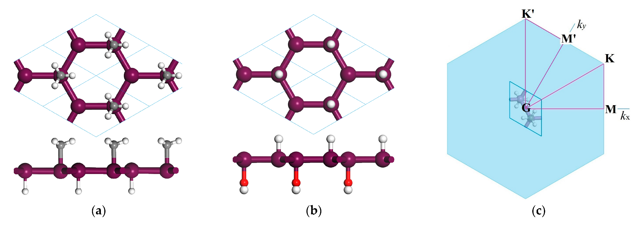
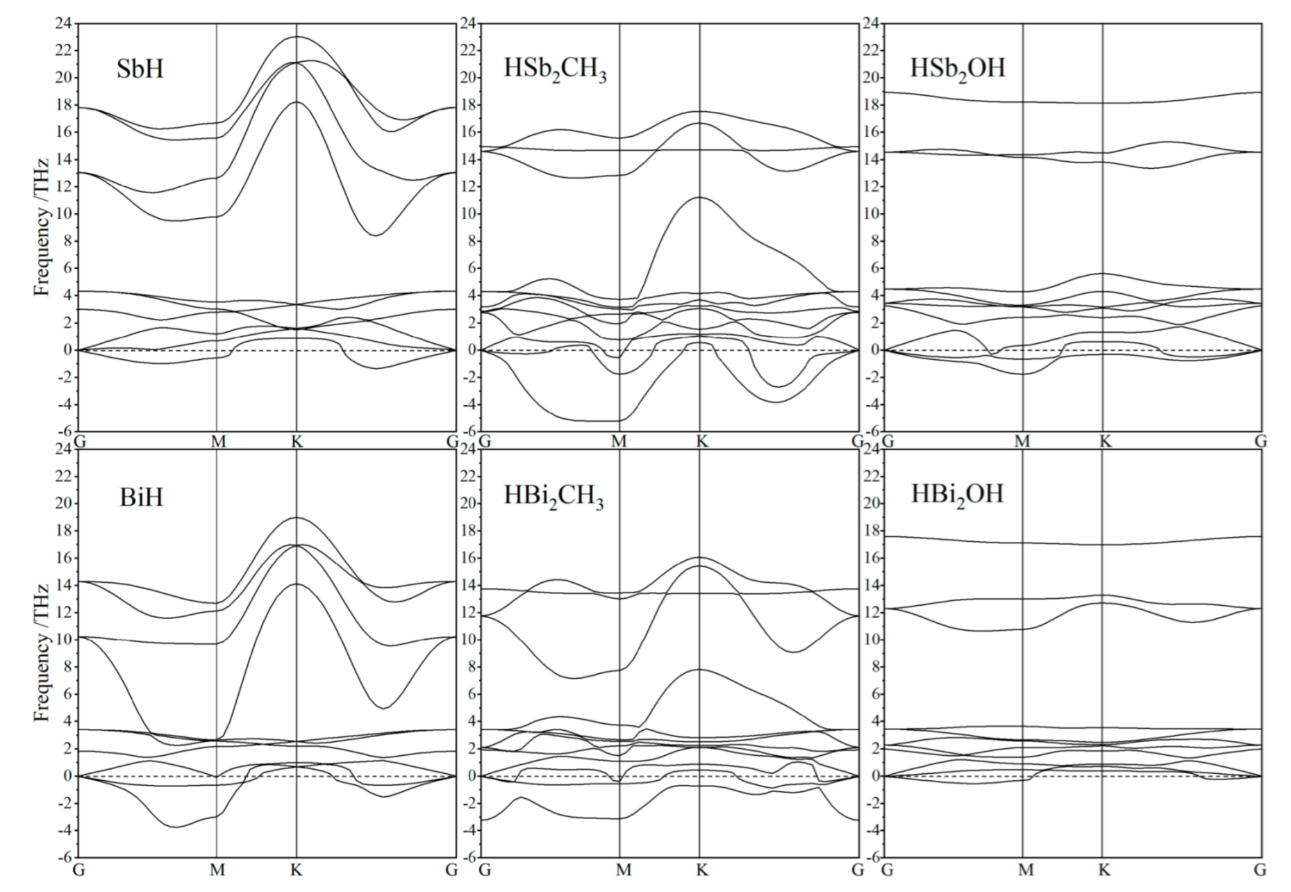
2.1. Atomic Geometry and Stability

Janus Sb or Bi monolayers (HSb2XHn and HBi2XHn, XHn = CH3, OH) are obtained by asymmetrical functionalizations (decorations) where the radical groups of methyl (CH3) and hydroxyl (OH) are bonded to Sb or Bi atoms on one surface side of Sb or Bi monolayer with the other surface side being saturated by hydrogen (H), as schematically shown in Figure 1, which possess space group of P3M1 in a threefold rotational symmetry of 2D honeycomb lattices. Compared with Sb or Bi and their hydrogen-saturated monolayers, the inversion symmetry has been broken for Janus Sb or Bi monolayers due to asymmetrical decoration. Lattice constants, bond lengths of Sb or Bi with center atoms of CH3 or OH, center buckle thickness, entire layer thickness, cohesive energy, Mulliken population charge of Janus Sb or Bi monolayers are listed in Table 1. We can see the appreciable buckle configurations of central Sb or Bi atomic layers for SbH or BiH monolayer and the quasi-planar geometry of Janus structures (for comparison). It has been demonstrated by preliminary calculations that the cohesive energy of the SbH or BiH monolayer (without chemical group decoration and no Janus) is higher than that of their purely elemental counterparts. Even though the bonding strength of Sb or Bi with C or O atoms is substantially higher than that with H atoms, the remarkably larger buckling of SbH and BiH monolayers leads to a comparable and even higher cohesive energy as that of Janus Sb and Bi monolayers, as shown in Table 1. The bonding strength, which is characterized by bond length and cohesive energy, increases with the increase in electronegativities of C and O elements. In particular, the cohesive energy approaches the highest and lowest values of 9.59 and 7.53 eV/unitcell for HSb2OH and HBi2CH3, respectively. It is an energetic indication that Janus Sb or Bi monolayers can be realized by strongly bonding CH3 or OH with Sb or Bi atomic layer into perfect crystalline structures. Thus, it is preferential to synthesize these asymmetrically functionalized monolayers with a high static stability in structure.
Kinetic stability under atomic oscillations is evaluated with frequency dispersion spectra of phonon modes, as shown in Figure 2. Preliminary phonon calculations by the linear response method [30] indicate that LO–TO frequencies at Brillouin zone center are degenerated for all these Janus and SbH or BiH monolayers, verifying that LO–TO splitting can be neglected. Phonon dispersion spectra of Janus Sb and Bi monolayers represent 12 branches comprised of three acoustic and nine optical branches. Acoustic phonon modes are classified into longitudinal acoustic waves, in-plane and out-of-plane transverse acoustic waves, while optical phonons contain an isolated out-of-plane transverse optical wave and a pair of G-point degenerated longitudinal and in-plane transverse optical waves. Both Janus Sb or Bi monolayers and SbH or BiH monolayers represent partially negative acoustic phonon frequencies in dispersion along G–M while approaching positive values near K point, which is attributed to virtual vibrations of H atoms passivating on Sb or Bi atomic layers. This result suggests that it is preferable to use other elements with a heavier mass and higher bonding strength rather than H atoms to saturate pz orbitals of Sb or Bi monolayers for complete kinetic stability.

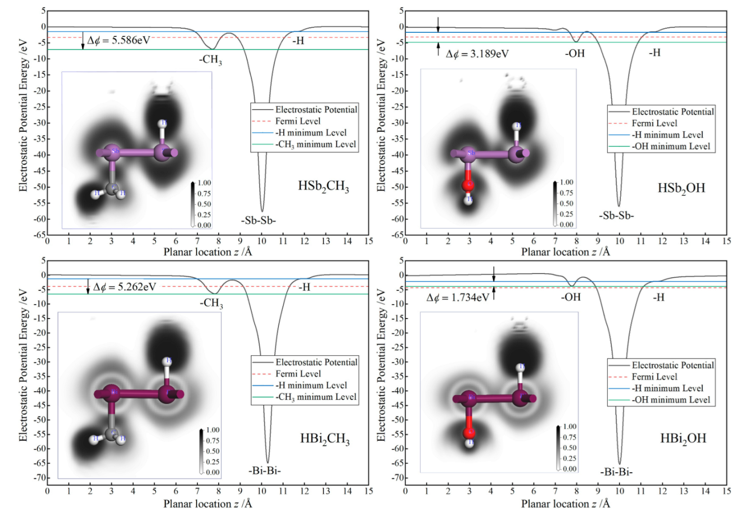
2.2. Internal Gradient of Electrostatic Potential
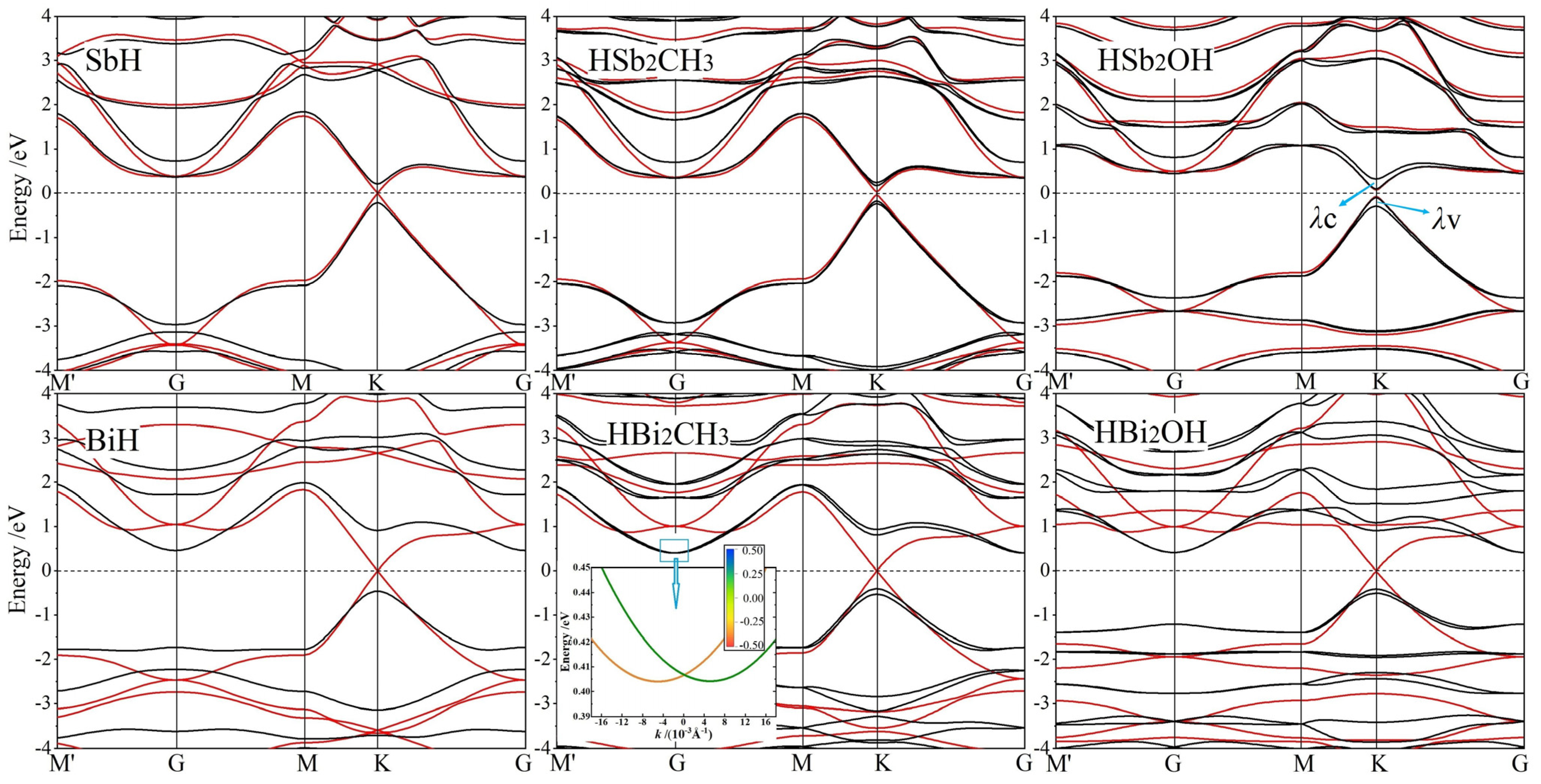
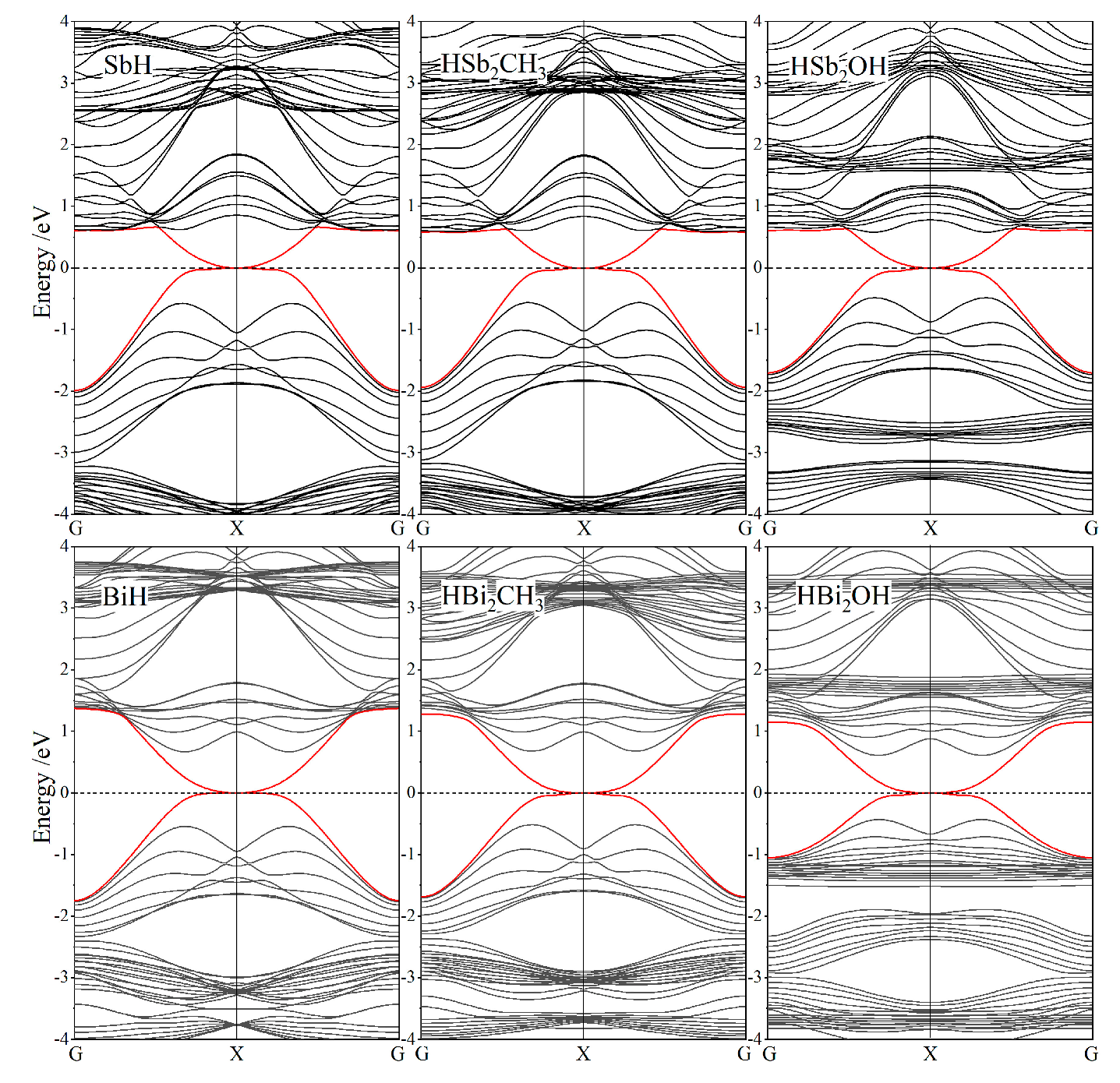
Mulliken population charges on the C and O bonding atoms of −0.5 and −0.7 e (or −0.9 and −1.3 e), respectively, due to their higher electronegativity than that of Sb (or Bi) are in contrast to −0.1 e (or 0.7 e) on hydrogen atoms directly bonding with Sb or Bi atoms, as listed in Table 1, implying substantial charge transfer and electronic cloud shifting out of central layer plane in Janus Sb and Bi monolayers. Accordingly, significant internal electric fields of Janus monolayers are created by the potential differences of ∆ϕ = 5.586, 3.179, 5.262 and 1.734 eV for HSb2CH3, HSb2OH, HBi2CH3 and HBi2OH, as shown in Figure 3. Therefore, it is suggested that inversion symmetry of Sb and Bi monolayers has been broken in these Janus monolayers due to the asymmetric decoration of CH3 or OH. For the Janus monolayers based on a heavy main group element, the electronegativity of center atoms in asymmetrically decorating chemical groups is a judgement giving rise to an intrinsic electric field.
Bonding characteristics of Sb or Bi with C or O atoms are evaluated by electron localization function (ELF), as depicted with the white–black contoured maps on the normal plane through atomic centers in the inserted panels of Figure 3. For all these Janus Sb and Bi monolayers, the highest ELF appears around the bonding middle between C atom center of CH3 and Sb or Bi atoms as a manifestation of covalent bonding in consistence with the minimal electron transfer according to Mulliken population charges. By contrast, for H or O atoms bonding with Sb or Bi atoms, the high ELF region resides around H or O center and promptly decreases at the middle of bonds, which implies ionic character, accounting for an internal electric field internal Janus Sb or Bi monolayers. ELF distributions reveal the chemical bonding attributes of the internal electric fields caused by asymmetrical functionalization with CH3 or OH.

2.3. Band Structure

All the band structures of Janus Sb and Bi monolayers from our calculations are merged in Figure 4, where the SOC effect could be distinguished by red and black dispersion curves. According to partial and atomic projections, it is determined that band-edge electronic-states near Fermi level are primarily composed of px and py orbitals from Sb or Bi bonding atoms [31]. Even without SOC, the highest valence band and the lowest conduction band crossing linearly at K and K′ points imply the Dirac-cone-like characteristics of these 2D honeycomb systems. When SOC is included, the degeneracy at Dirac-cone point splits off with the highest valence band and the lowest conduction band shifted towards high and low energy from Fermi level, respectively, thereby opening a notable band-gap by SOC for both the symmetrically hydrogenated and Janus monolayers. By contrast, at G point, the valence and conduction bands are upshifted and downshifted respectively, which accounts for a global indirect band-gap in the functionalized Bi monolayers with a remarkably larger K-point splitting caused by a much stronger SOC of Bi systems than that of Sb systems. Global band-gaps of Janus Sb and Bi monolayers range in 0.2~0.4 eV and 0.8~0.9 eV, respectively, as listed in Table 2.
It has been reported by ab-initio calculations that Rashba spin-splitting occurs in all the Janus Mo and W dichalcogenide monolayers due to the simultaneous existences of strong SOC and internal electric field. Consistently, Rashba spin-splitting arises in HBi2CH3 monolayers with a built-in potential gradient as shown in Figure 3, leading to a perceptible Rashba parameter RG of 0.224 eV·Å due to the strong SOC from px and py orbitals of Bi bonding atoms, as manifested by comparing non-SOC and SOC band structures in Figure 4. It is suggested by the lower built-in electric field in Rashba splitting HBiCH3 than in HSb2CH3 with a lower SOC that strong SOC dominates the generation of Rashba splitting in Janus Sb and Bi monolayers. Since SOC and angular momentum cannot be simultaneous represented in quantum mechanics, the spin-up and spin-down states cannot be completely determined in SOC band structures, as shown by the color-mapped spin components near Fermi level for Rashba HBiCH3 monolayer in the inserted panel of Figure 4. Meanwhile, SOC also causes remarkable band-edge splittings at K point for Janus Sb and Bi monolayers, as indicated by λv and λc for the upmost valence band and the downmost conduction band, respectively, with the values listed in Table 2. For HBi2CH3 and HBi2OH monolayers, the valley shape of the upmost valence band is preferred over the flat shape of the downmost conduction band at K point for valleytronics applications.
Topological properties of SbH and BiH monolayers are characterized by the topological Z2 invariant evaluated from first-principles electronic Bloch wave-functions, where Z2 = 1 and Z2 = 0 represent the nontrivial and trivial topology, respectively. Since the atomic structures of SbH and BiH monolayers have space inversion symmetry, the Z2 topological invariant is directly calculated by Bloch wave-function parities of valence electrons at time-reversal-invariant points (TRIPs) in Brillouin zone. Electronic structures of SbH and BiH monolayers have four TRIPs, one at G point and three at M point, so the topological index P can be calculated as follows:
P ( K i ) = m = 1 N δ 2 m i , ( 1 ) ν = i = 1 4 P ( K i ) = P ( G ) P ( M ) 3
where P denotes the parity product of Bloch wave-functions on TRIPs, δ = ±1 indicates parity, and N is the number of valence bands. The 12 valence electrons in primitive cells of SbH or BiH monolayer constitute six spin-degenerate electronic-states at a TRIP, and the parities of spin-degenerate electron eigenfunctions of SbH and BiH monolayers on all TRIPs are identical. As shown in Table 3, the values of P at G and M points are –1 and +1 respectively, which leads to the nontrivial Z2 = 1, demonstrating that SbH and BiH monolayers are nontrivial topological insulators.
In contrast, it is invalid of evaluating Z2 invariant by the parity of valence electronic-states to determine whether Janus Sb and Bi monolayers are topologically trivial or nontrivial, because they are lacking of space inversion symmetry due to the asymmetrical functionalization of chemical groups. Nevertheless, nontrivial topology of Janus Sb and Bi monolayers could be represented in the odd number of conductive channels from edge electronic-states without band-gap, where Dirac-cone point appears to be crossed by the lowest conduction band and the highest valence band of nanoribbon at Fermi level. To investigate this important topological property, the zigzag nanoribbons of Janus Sb and Bi monolayers are constructed, in which atomic structures on both edges are mirror-symmetrical to each other, and the unsaturated edge bonds are passivated by hydrogen atoms. Nanoribbon width is specified about 35 Å to avoid overlapping between two edge states of nanoribbon. After geometrical optimization, the band structures of Janus Sb and Bi monolayer nanoribbons are calculated, with the results shown in Figure 5. The energy dispersion of edge electronic-states of these nanoribbons intersects into a Dirac-cone point of Fermi level at boundary X point of one-dimensional Brillouin zone. The odd number of edge-state conductance channels is derived from nontrivial topology that will also present edge-state Dirac-cones in band structures of armchair nanoribbons. Therefore, this Dirac-cone signature of edge states proves these Janus Sb and Bi monolayers are (nontrivial) topological insulators to realize QSH effect at ambient temperature supported by their giant band-gaps.

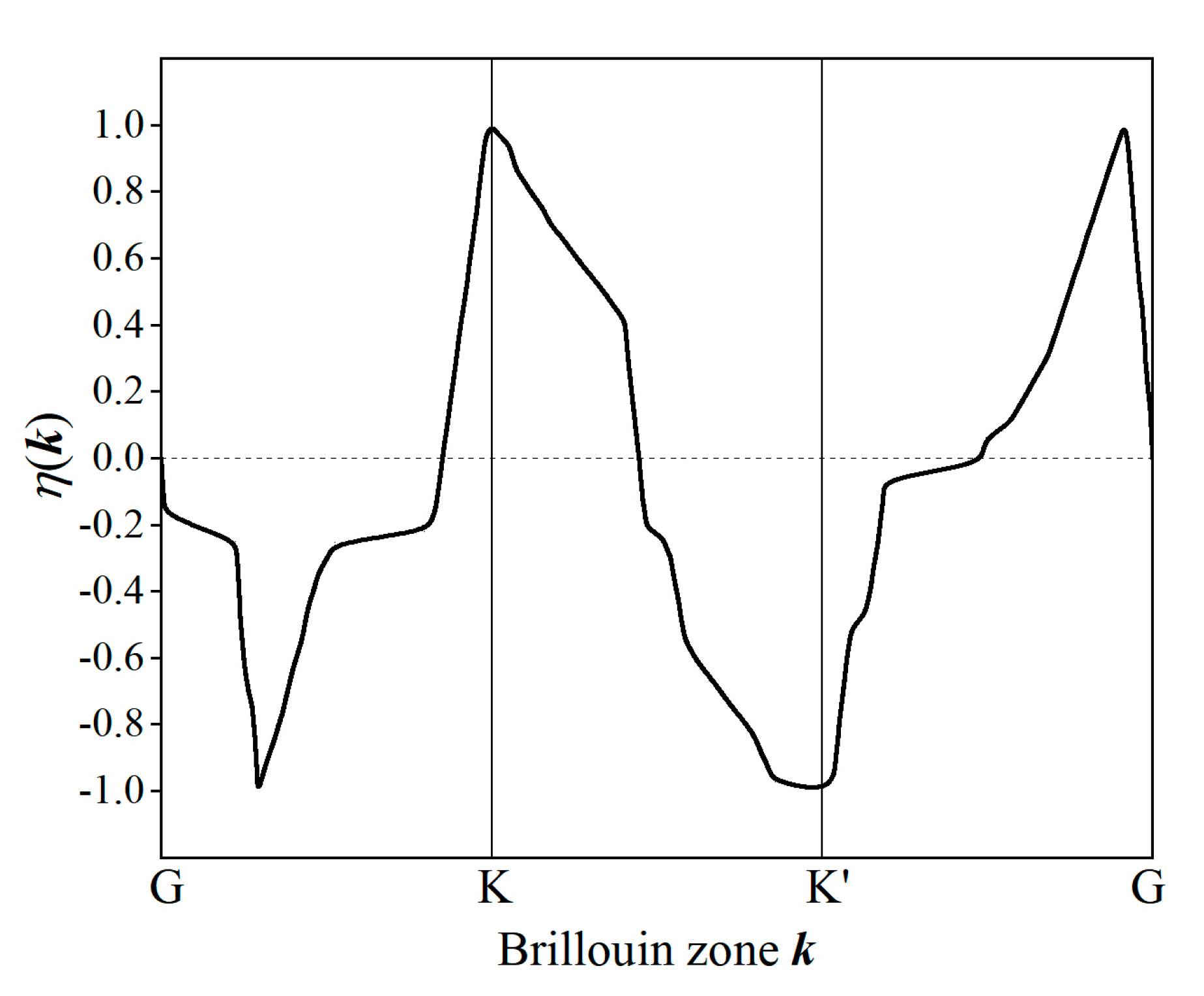
2.4. Valley-Contrast Circular Dichroism

There is a valley degree of freedom in Janus Sb and Bi monolayers, and the strong SOC opens a large electronic energy gap at the corners of Brillouin zone. Inversion symmetry is broken in Janus Sb and Bi monolayers due to the asymmetrical functionalizations with CH3 or OH, leading to valley-contrast Berry curvature and spin that yield valley spin Hall effect and valley-contrast circular dichroism. With a giant bulk band-gap and nontrivial topology, these Janus monolayers can afford to be a quantum spin Hall insulator and a quantum valley Hall insulator at ambient temperature. Valley-contrast Berry curvature and spin can be described by valley polarization η(k) in Brillouin zone as follows:
η ( k ) = | P + ( k ) | 2 | P ( k ) | 2 | P + ( k ) | 2 + | P ( k ) | 2 , P ± = P x ± i P y
where Pα (α = x, y) denotes momentum matrix element between the lowest conduction band and the highest valence band. Prototypically, the calculated η(k) of HBi2OH monolayer along the high-symmetry path through valley K and K′ points in Brillouin zone is shown in Figure 6, illustrating the contrast of optical selection rule between two valley counterparts. The left-hand and right-hand circular polarized photons are almost purely absorbed at K and K′ valleys, respectively. Therefore, circular polarized photons can distinguish electronic excitation and imbalance electron occupation between the two inversely distributed nonequivalent electronic-valleys in Janus Sb and Bi monolayers without external electric field.
According to a low-power model, the valley magnetic moments in Janus Sb and Bi monolayers are related to both valley pseudo-spin and real spin which are substantially coupled due to giant band-gaps induced by strong SOC. Valley pseudo-spin can be rendered by strong SOC under the internal built-in electric field in Janus Sb and Bi monolayers, which is different from inversion symmetry systems that need an external electric field. Notably, valleytronics can hardly be achieved due to minimal SOC in graphene or silicene, whilst requires a high external electric field to break inversion symmetry in SbH and BiH monolayers.

3. Theoretical Methodology

Employing the fully relativistic pseudopotential planewave first-principles method based on spin density functional theory, the atomic structure, phonon dispersion, SOC electronic structures of Janus Sb and Bi monolayers are calculated as implemented by CASTEP module of Materials Studio 2020 package (Accelrys Inc., Materials Studio version 2020.08, San Diego, CA, USA) [32]. Gradient-corrected exchange–correlation functional Wu and Cohen (WC) is adopted to perform the electronic state and energy calculations [33]. WC functional has been shown to achieve a significant improvement over LDA, PBE and TPSS functionals for predicting atomic structures of solids including ionic compounds and describing covalent bonds of molecules, especially for group I, group IV and group III–V semiconductors [34]. SOC is incorporated into the calculations of energy, atomic force and geometry, electronic structure and optoelectronic matrix elements. Band structures without SOC are also calculated for comparison to reveal the SOC-induced source of Rashba splitting, valley freedom and giant band-gaps.
Interactions between atomic cores and valence electrons are presented by norm-conserving pseudopotential, and the relativistic effect is treated with Koelling–Harmon schemes [35]. Electron wave functions are expanded by plane-wave basis-set under 720 eV energy cutoff, whilst finite basis-set correction is used in energy and stress calculations by estimating energy derivatives from three-points numerical differentiation [36]. Pulay density mixing scheme at 0.5 charge magnitude is utilized to carry out self-consistent field (SCF) iterations with a convergence tolerance of 5 × 10⁻⁷ eV/atom and on an FFT grid of 48 × 48 × 200 for electron density calculations [37,38]. Monkhorst–Pack 3 × 3 × 1 grid of k-sampling is adopted for integration in Brillouin zone [39].
Two-dimensional atomic structures are modeled in virtual three-dimensional space by setting a sufficient vacuum layer (15 Å) between the periodic images of monolayers. Geometry optimization is fulfilled by minimizing energy functional with BFGS algorithm in delocalized internal coordinates instead of Cartesian coordinates, so as to reach the energy, atomic force and stress convergences of 5.0 × 10⁻⁶ eV/atom, 0.01 eV/Å and 0.02 GPa, respectively [40]. Phonon structures are calculated by finite-displacement method using several small supercells without SOC-induced bonding force and ignoring frequency splitting between the longitude and transverse optical vibration modes (LO–TO splitting) at G point, in which the convergence tolerance of mechanical constant is specified as 1.0 × 10⁻⁵ eV/Å2.

4. Conclusions

Spin–orbit coupling electronic structures of Janus (asymmetrically functionalized by CH3 or OH) Sb and Bi monolayers (HSb2XHn and HBi2XHn) with nontrivial topology, Rashba splitting and valley-contrast circular dichroism are first proposed and demonstrated in the present study. Cohesive energies and phonon dispersion indicate that all these Janus systems have innate static stability, whilst undergoing kinetic instability of H atoms capping another surface of Sb or Bi atomic layer. Under SOC effects, Janus Sb and Bi monolayers show direct and indirect band-gap characteristics of band structures, respectively. It is identified by means of first-principles calculations that HSb2XHn and HBi2XHn are a new family of giant band-gap 2D TIs with the largest bulk band-gap of ~0.8 eV, by far exceeding the current band-gaps of 2D TI materials realized in experiments. These giant band-gaps are entirely attributed to strong SOC of Sb or Bi px and py atomic orbitals around K and K′ valleys in Brillouin zone of honeycomb lattice, which suffice for practical applications at ambient temperature. Rashba splitting originates dominantly from strong SOC together with built-in out-of-plane electric field, as manifested by the unique Rashba HBi2CH3 monolayer possessing strong SOC but with a minimal out-of-plane potential gradient. Janus Sb and Bi monolayers are identified to be a spin valley Hall insulator by valley-selective circular dichroism. Due to strong SOC, the valley magnetic moments could be modified by intrinsic out-of-plane electric field to produce a substantial correlation between real and valley-pseudo spins. These results represent a significant advance in 2D TIs to stimulate further work of developing these new 2D TIs for Rashba spintronic devices and quantum valley Hall insulators.

Author Contributions

Data curation, formal analysis, writing—original draft preparation, writing—review and editing, Q.G.; conceptualization, investigation, project administration, G.Z. All authors have read and agreed to the published version of the manuscript.

Funding

This research was funded by the National Natural Science Foundation of China (Grant No. 51973046).

Institutional Review Board Statement

Not applicable.

Informed Consent Statement

Not applicable.

Data Availability Statement

Theoretical methods and results are available from all authors.

Conflicts of Interest

The authors declare no conflict of interest.

References

  1. Salem, A.K.; Searson, P.C.; Leong, K.W. Multifunctional nanorods for gene delivery. Nat. Mater. 2003, 2, 668–671. [Google Scholar] [CrossRef] [PubMed]
  2. Roh, K.H.; Martin, D.C.; Lahann, J. Biphasic Janus particles with nanoscale anisotropy. Nat. Mater. 2005, 4, 759–763. [Google Scholar] [CrossRef] [PubMed]
  3. Nisisako, T.; Hatsuzawa, T. A microfluidic cross-flowing emulsion generator for producing biphasic droplets and anisotropically shaped polymer particles. Microfluid. Nanofluid. 2010, 9, 427–437. [Google Scholar] [CrossRef]
  4. Zhang, L.; Luo, Q.; Zhang, F.; Zhang, D.M.; Wang, Y.S.; Sun, Y.L.; Dong, W.F.; Liu, J.Q.; Huo, Q.S.; Sun, H.B. High-performance magnetic antimicrobial Janus nanorods decorated with Ag nanoparticles. J. Mater. Chem. 2012, 22, 23741–23744. [Google Scholar] [CrossRef]
  5. Kirillova, A.; Schliebe, C.; Stoychev, G.; Jakob, A.; Lang, H.; Synytska, A. Hybrid hairy Janus particles decorated with metallic nanoparticles for catalytic applications. ACS Appl. Mater. Interfaces 2015, 7, 21218–21225. [Google Scholar] [CrossRef]
  6. Zhang, L.; Yu, J.; Yang, M.; Xie, Q.; Peng, H.; Liu, Z. Janus graphene from asymmetric two-dimensional chemistry. Nat. Commun. 2013, 4, 1443. [Google Scholar] [CrossRef] [Green Version]
  7. Bissett, M.A.; Takesaki, Y.; Tsuji, M.; Ago, H. Increased chemical reactivity achieved by asymmetrical ‘Janus’ functionalisation of graphene. RSC Adv. 2014, 4, 52215–52219. [Google Scholar] [CrossRef]
  8. Li, F.; Li, Y.F. Band gap modulation of Janus graphene nanosheets by interlayer hydrogen bonding and the external electric field: A computational study. J. Mater. Chem. C 2015, 3, 3416–3421. [Google Scholar] [CrossRef]
  9. Chico, L.; Latgé, A.; Brey, L. Symmetries of quantum transport with Rashba spin-orbit: Graphene spintronics. Phys. Chem. Chem. Phys. 2015, 17, 16469–16475. [Google Scholar] [CrossRef] [PubMed] [Green Version]
  10. Lv, M.H.; Li, C.M.; Sun, W.F. Spin-orbit coupling and spin-polarized electronic structures of Janus vanadium-dichalcogenide monolayers: First-principles calculations. Nanomaterials 2022, 12, 382. [Google Scholar] [CrossRef]
  11. Hu, W.; Xia, N.; Wu, X.J.; Li, Z.Y.; Yang, J.L. Silicene as a highly sensitive molecule sensor for NH3, NO and NO2. Phys. Chem. Chem. Phys. 2014, 16, 6957–6962. [Google Scholar] [CrossRef]
  12. Kaloni, T.P.; Schreckenbach, G.; Freund, M.S. Large enhancement and tunable band gap in silicene by small organic molecule adsorption. J. Phys. Chem. C 2014, 118, 23361–23367. [Google Scholar] [CrossRef] [Green Version]
  13. Özçelik, V.O.; Kecik, D.; Durgun, E.; Ciraci, S. Adsorption of group IV elements on graphene, silicene, germanene, and stanene: Dumbbell formation. J. Phys. Chem. C 2015, 119, 845–853. [Google Scholar] [CrossRef] [Green Version]
  14. Denis, P.A. Stacked functionalized silicene: A powerful system to adjust the electronic structure of silicene. Phys. Chem. Chem. Phys. 2015, 17, 5393–5402. [Google Scholar] [CrossRef] [PubMed]
  15. Yu, W.Z.; Yan, J.A.; Gao, S.P. Band gap characters and ferromagnetic/antiferromagnetic coupling in group-IV monolayers tuned by chemical species and hydrogen adsorption configurations. Nanoscale Res. Lett. 2015, 10, 351. [Google Scholar] [CrossRef] [PubMed] [Green Version]
  16. Qiu, J.; Fu, H.; Xu, Y.; Zhou, Q.; Meng, S.; Li, H.; Chen, L.; Wu, K. From silicene to half-silicane by hydrogenation. ACS Nano 2015, 9, 11192–11199. [Google Scholar] [CrossRef] [PubMed]
  17. Zhang, W.B.; Song, Z.B.; Dou, L.M. The tunable electronic structure and mechanical properties of halogenated silicene: A first-principles study. J. Mater. Chem. C 2015, 3, 3087–3094. [Google Scholar] [CrossRef]
  18. Özçelik, V.O.; Cahangirov, S.; Ciraci, S. Stable single-layer honeycomblike structure of silica. Phys. Rev. Lett. 2014, 112, 246803. [Google Scholar] [CrossRef] [Green Version]
  19. Stephan, R.; Hanf, M.C.; Sonnet, P. Opening the way to molecular cycloaddition of large molecules on supported silicene. J. Chem. Phys. 2015, 143, 154706. [Google Scholar] [CrossRef]
  20. Wu, J.; Xie, L.M.; Li, Y.; Wang, H.; Ouyang, Y.; Guo, J.; Dai, H.G. Controlled chlorine plasma reaction for noninvasive graphene doping. J. Am. Chem. Soc. 2011, 133, 19668–19671. [Google Scholar] [CrossRef]
  21. Freitas, R.R.Q.; Rivelino, R.; de Brito Mota, F.; de Castilho, M.C. Topological insulating phases in two-dimensional bismuth containing single layers preserved by hydrogenation. J. Phys. Chem. C 2015, 119, 23599–23606. [Google Scholar] [CrossRef] [Green Version]
  22. Liu, C.C.; Jiang, H.; Yao, Y.G. Low-energy effective Hamiltonian involving spin-orbit coupling in silicene and two-dimensional germanium and tin. Phys. Rev. B 2011, 84, 195430. [Google Scholar] [CrossRef] [Green Version]
  23. Liu, C.C.; Feng, W.X.; Yao, Y.G. Quantum spin Hall effect in silicene and two-dimensional germanium. Phys. Rev. Lett. 2011, 107, 076802. [Google Scholar] [CrossRef] [PubMed] [Green Version]
  24. Wang, Z.F.; Liu, Z.; Liu, F. Organic topological insulators in organometallic lattices. Nat. Commun. 2013, 4, 1471. [Google Scholar] [CrossRef] [PubMed] [Green Version]
  25. Xu, Y.; Yan, B.; Zhang, H.J.; Wang, J.; Xu, G.; Tang, P.; Duan, W.; Zhang, S.C. Large-gap quantum spin Hall insulators in tin films. Phys. Rev. Lett. 2013, 111, 136804. [Google Scholar] [CrossRef]
  26. Yang, F.; Miao, L.; Wang, Z.F.; Yao, M.Y.; Zhu, F.; Song, Y.R.; Wang, M.X.; Xu, J.P.; Fedorov, A.V.; Sun, Z.; et al. Spatial and energy distribution of topological edge states in single Bi(111) bilayer. Phys. Rev. Lett. 2012, 109, 016801. [Google Scholar] [CrossRef] [Green Version]
  27. Yan, B.H.; Jansen, M.; Felser, C. A large-energy-gap oxide topological insulator based on the superconductor BaBiO3. Nat. Phys. 2013, 9, 709–711. [Google Scholar] [CrossRef] [Green Version]
  28. Gong, Q.; Zhang, G. Spin-orbit coupling electronic structures of organic-group functionalized Sb and Bi topological monolayers. Nanomaterials 2022, 12, 2041. [Google Scholar] [CrossRef]
  29. Klintenberg, M.; Lebegue, S.; Katsnelson, M.; Eriksson, O. Theoretical analysis of the chemical bonding and electronic structure of graphene interacting with group IA and group VIIA elements. Phys. Rev. B 2010, 81, 085433. [Google Scholar] [CrossRef] [Green Version]
  30. Baroni, S.; de Gironcoli, S.; dal Corso, A.; Giannozzi, P. Phonons and related crystal properties from density-functional perturbation theory. Rev. Mod. Phys. 2001, 73, 515–562. [Google Scholar] [CrossRef] [Green Version]
  31. Ma, Y.D.; Dai, Y.; Kou, L.Z.; Frauenheim, T.; Heine, T. Robust two-dimensional topological insulators in methyl functionalized bismuth, antimony, and lead bilayer films. Nano Lett. 2015, 15, 1083–1089. [Google Scholar] [CrossRef] [PubMed]
  32. Clark, S.J.; Segall, M.D.; Pickard, C.J.; Hasnip, P.J.; Probert, M.I.J.; Refson, K.; Payne, M.C. First principles methods using CASTEP. Z. Krist. 2005, 220, 567–570. [Google Scholar] [CrossRef] [Green Version]
  33. Wu, Z.; Cohen, R.E. More accurate generalized gradient approximation for solids. Phys. Rev. B 2006, 73, 235116. [Google Scholar] [CrossRef] [Green Version]
  34. Tran, F.; Laskowski, R.; Blaha, P.; Schwarz, K. Performance on molecules, surfaces, and solids of the Wu-Cohen GGA exchange-correlation energy functional. Phys. Rev. B 2007, 75, 115131. [Google Scholar] [CrossRef] [Green Version]
  35. Lin, J.S.; Qteish, A.; Payne, M.C.; Heine, V. Optimized and transferable nonlocal separable ab initio pseudopotentials. Phys. Rev. B 1993, 47, 4174–4180. [Google Scholar] [CrossRef] [PubMed]
  36. Milman, V.; Lee, M.H.; Payne, M.C. Ground-state properties of CoSi2 determined by a total-energy pseudopotential method. Phys. Rev. B 1994, 49, 16300–16308. [Google Scholar] [CrossRef]
  37. Payne, M.C.; Teter, M.P.; Allan, D.C.; Arias, T.A.; Joannopoulos, J.D. Iterative minimization techniques for ab initio total energy calculations: Molecular dynamics and conjugate gradients. Rev. Mod. Phys. 1992, 64, 1045–1097. [Google Scholar] [CrossRef] [Green Version]
  38. Kresse, G.; Furthmuller, J. Efficient iterative schemes for ab initio total-energy calculations using a plane-wave basis set. Phys. Rev. B 1996, 54, 11169–11186. [Google Scholar] [CrossRef]
  39. Monkhorst, H.J.; Pack, J.D. Special points for Brillouin-zone integrations—A reply. Phys. Rev. B 1977, 16, 1748. [Google Scholar]
  40. Packwood, D.; Kermode, J.; Mones, L.; Bernstein, N.; Woolley, J.; Gould, N.; Ortner, C.; Csanyi, G. A universal preconditioner for simulating condensed phase materials. J. Chem. Phys. 2016, 144, 164109. [Google Scholar] [CrossRef] [Green Version]
Figure 1. (a,b) Top-view (top) and side-view (bottom) schematics of Janus Sb or Bi monolayers with asymmetrical decorations of H and CH3 or OH on two surface sides, respectively, where the violet, gray, red and white balls symbolize the bonding atoms of Sb or Bi, C, O and H, respectively; (c) high-symmetry points (M, K, M′, K′) specifying the dispersion paths of phonon frequency or electron energy in Brillouin zone.
Ijms 23 07629 g001
Figure 2. Phonon dispersion spectra of Janus Sb and Bi monolayers in comparison to SbH and BiH monolayers.
Ijms 23 07629 g002
Figure 3. Internal potential gradient and bonding characteristics of the Janus Sb and Bi monolayers: mean electrostatic potential as a function of the planar position, with the inserted panels showing the electron localization function contoured on the normal plane crossing both Sb or Bi and C or O atomic centers.
Ijms 23 07629 g003
Figure 4. Band structures without SOC (red curves) and with SOC (black curves) of Janus Sb (top panels) and Bi (bottom panels) monolayers, and SbH and BiH monolayers with inversion symmetry are presented for comparison, in which Fermi level is referenced as energy zero (horizontal dash line).
Ijms 23 07629 g004
Figure 5. SOC-included band structures of zigzag nanoribbons of Janus Sb and Bi monolayers (functionalized asymmetrically by H atom and CH3 or OH), and SbH and BiH nanoribbons are presented for comparison, with red color indicating edge states and Fermi level being referenced as energy zero.
Ijms 23 07629 g005
Figure 6. Valley polarization of HBi2OH monolayer along high-symmetry path through valley K and K′ points.
Ijms 23 07629 g006
Table 1. Lattice constants a, bond lengths of Sb or Bi with center atoms of CH3 or OH (dMX), center buckle thickness (hM), entire layer thickness (h), cohesive energy (Ecoh), Mulliken population charge (qM) where M1 and M2 indicate two atoms of Sb or Bi and X denotes the functional-group center atom (C or O) or the H atom (for SbH and BiH only) of Janus Sb and Bi monolayers together with the SbH and BiH monolayers for comparison.
MonolayersadMXhMhEcoh/eV·unitcell−1qM/e
M1M2X
SbH5.2181.7190.0923.3469.4090.130.13−0.13
HSb2CH35.2072.1730.0034.2529.2450.290.09−0.53
HSb2OH5.2191.9120.0034.5969.5910.71−0.13−0.71
BiH5.4671.8510.1753.5267.7710.730.73−0.73
HBi2CH35.4782.3330.0464.4757.5341.080.48−0.93
HBi2OH5.4942.1200.0344.6567.6191.180.46−1.32
Table 2. Rashba spin-splitting RG of the highest valence band at G point, SOC-induced splitting λv and λc at K point for valence and conduction band-edges respectively, SOC-induced Dirac-cone splitting gaps at K point ED(K), global band-gaps Eg(global) of Janus Sb and Bi monolayers compared with SbH and BiH monolayers.
MonolayersRG/eV·Åλv/meVλc/meVED(K)/eVEg(global)/eV
SbH0000.4260.426
HSb2CH300.0600.0650.3510.351
HSb2OH00.1940.2290.1940.194
BiH0001.3720.918
HBi2CH30.2240.1240.1231.2190.809
HBi2OH00.0930.1771.3230.824
Table 3. Parities δ and their product P of spin-degenerate states at TRIPs for SbH and BiH monolayers.
TRIPParity δP
G+1+1−1+1−1+1−1
3 M+1−1+1−1+1−1+1
Publisher’s Note: MDPI stays neutral with regard to jurisdictional claims in published maps and institutional affiliations.

