Abstract
MXene is widely used in the fields of microwave absorption and electromagnetic shielding to balance electromagnetic pollution with the development of communication technologies and human health, due to its excellent surface functional groups and tunable electronic properties. Although pure multilayered MXene has an excellent accordion-like structure, the weak dielectric loss and lack of magnetic loss result in poor microwave absorption performance. Here, we propose a strategy for the catalytic growth of CNTs by the electrophoretic deposition of adsorbed metal ions, leading to the successful preparation of Ni-MWCNTs/Ti3C2Tx composites with a “layer-by-layer” structure, achieved through in situ regulated growth of CNTs. By introducing dielectric–magnetic synergy to improve the impedance matching conditions, and by regulating the diameter of the CNTs to alter the electromagnetic parameters of Ni-MWCNTs/Ti3C2Tx, the 2-Ni-MWCNTs/Ti3C2Tx composite achieves the best reflection loss (RL) value of −44.08 dB and an effective absorption bandwidth of 1.52 GHz at only 2.49 mm thickness. This unique layered structure and the regulation strategy provide new opportunities for the development of few-layered MXene composites.
1. Introduction
The rapid development of radio communication and electronic devices, as well as the widespread use of electromagnetic wave pollution, poses increasing threats to human health. Precision instruments and information security are also vulnerable to electromagnetic wave interference. Therefore, the study of advanced electromagnetic wave absorbing materials to cope with the complex electromagnetic environment has become urgent [1,2,3,4,5]. Ideal electromagnetic wave-absorbing materials should have a thin thickness, a wide absorption bandwidth, a strong absorption capacity, and be lightweight [6,7]. Currently, traditional microwave absorbing materials (MAMs), such as carbon-based materials [8], conducting polymers [9], ceramics, and magnetic metal powders [10], have struggled to fulfill all four of these requirements simultaneously. In the process of exploring new materials, researchers have discovered that the properties of two-dimensional nanomaterials, such as good electrical conductivity, a large specific surface area, rich functional groups, high mechanical strength, stability, and special structures that enable strong dielectric loss and multiple reflections [2,11,12]. These characteristics make them a promising candidate for microwave-absorbing applications.
Compared to other 2D materials, such as TMDs [13], h-BN [14,15], and graphene [16,17], MXene exhibits a higher electrical conductivity, specific surface area, and tunable electronic properties [18,19,20,21]. Its rich variety of surface functional groups and its layered structure, which are conducive to prolonged electromagnetic wave absorption, have garnered increasing attention in the field of microwave absorption (MA). In recent years, although MXene has been extensively studied, its overall MA performance is still greatly limited by its single microwave absorption mechanism, high relative complex dielectric constant, and low relative complex permeability constant. To further enhance its MA characteristics and adaptability, MXene-based composites have been developed by adjusting the composition and structural design to obtain MAMs with exceptional properties. For example, heterogeneous interfacial structures [22], dielectric–magnetic synergies [23], porous structures [24], and hyperstructures [25] have all been explored. Carbon-based materials primarily include 1D carbon nanotubes, 2D graphene [26], and 3D carbon nanospheres, which are common high dielectric loss materials. These materials have found numerous applications in the preparation of heterogeneous interfaces and high conductive loss MXene/carbon matrix composites [27,28]. The composites of one-dimensional (1D) carbon nanotubes make them more prominent in generating conductive networks and conduction loss, contributing to a higher conductive loss and polarization loss at lower amounts [17]. Magnetic transition metal atoms (such as Co, Fe, and Ni) are commonly used as catalysts to catalyze the in situ synthesis of CNTs [29,30], ensuring catalytic growth at lower temperatures while preventing oxidation of the substrate material and structural collapse caused by phase transitions. Che et al. [31] investigated the fabrication of a magnetic CNTs/Ni heterostructure decorated on an MXene substrate via a facile in situ induced growth method. Impedance matching conditions are improved by increasing interface polarization and magnetic loss through dielectric–magnetic synergy and the heterogeneous interface structure, resulting in superior microwave absorption performance of −56.4 dB at only 2.4 mm thickness. The excellent wave-absorbing performance benefits from the 3D porous structure and the dielectric–magnetic synergy. Notably, most of the MXene-based wave-absorbing materials reported so far are still multilayered MXene, while fewer studies have focused on few-layered MXene. Few-layered MXene is susceptible to self-aggregation and accumulation during assembly due to Van der Waals forces and hydrogen bonding, which reduces their stability and MA performance [32]. Furthermore, few-layered MXene has better electrical conductivity than multilayered MXene [31], and lacks the accordion-like structure found in multilayer MXenes, leading to an impedance mismatch. As a result, most electromagnetic waves are reflected away from the wave-absorbing material rather than being absorbed. Regulating the balance between the high dielectric loss and the impedance mismatch to improve impedance matching remains a significant challenge.
Herein, we propose an electrophoretic deposition strategy for the adsorption of metal catalytic ions. Ni-MWCNTs/Ti3C2Tx materials with excellent wave-absorbing properties were successfully prepared by modulating the in situ growth of CNTs. During the deposition of few-layered MXene, metal catalytic ions are adsorbed between the layers and on the surface. The growth of CNTs after annealing effectively prevents the self-aggregation and accumulation of MXene during the assembly process. Additionally, the introduction of metal magnetic atoms enhances the magnetic loss and creates dielectric–magnetic synergy. The interfacial polarization loss and conductivity loss of Ni-MWCNTs/Ti3C2Tx composites are controlled by adjusting the tube diameter of CNTs to improve the impedance matching conditions. This work contributes fresh concepts for the structural design of MXene-based materials and 2D nanomaterials.
2. Results and Discussion
2.1. Preparation and Characterization of Ni-MWCNTs/Ti3C2Tx Composites
The preparation of Ni-MWCNTs/Ti3C2Tx is shown in Figure 1a. Firstly, a few-layered Ti3C2Tx MXene suspension was generated by in situ hydrofluoric acid etching of the MAX phase Ti3AlC2 (Figure S1a). The zeta potential was −36.65 mV (Figure S1b), which is attributed to the presence of negatively charged -F, -Cl, and -OH functional groups on the surface. The greater the absolute value of the zeta potential (greater than 30 mV), the more stable the solution [33], which favors the directional movement of the suspension under the influence of the electric field. Electrophoretic deposition (EPD) was then carried out, using the few-layered Ti3C2Tx solution as the electrolyte, with graphite rods and Ni flakes serving as the cathode and anode, respectively. The Ti3C2Tx nanoflakes were deposited on Ni flakes as the negatively charged surface moved toward the anode under the applied voltage. The Ti3C2Tx nanoflakes were deposited onto the Ni flakes due to the negatively charged surface, which moved directionally toward the anode under the influence of the applied voltage. At the anode, the Ni flakes undergo an oxidation reaction, generating a high concentration of Ni2+ via dissolution around them. This Ni2+ is then adsorbed onto the interlayers and surfaces of the Ti3C2Tx nanosheets as they are deposited towards the anode, forming a Ni2+-Ti3C2Tx composite. Next, carbon nanotube (CNT) growth was initiated using low-pressure thermochemical vapor deposition (LPTCVD) at 550 °C with cracked acetylene as the carbon source. In the presence of Ni nanoparticles (which are fully reduced from Ni2+ to Ni monomers in H2 at 400 °C for 30 min to serve as active catalytic sites), carbon atoms near the interlayer and surface of Ti3C2Tx are rearranged to catalyze the growth of CNTs. The interlayer-grown CNTs are well-connected along the Z-axis to several layers of deposited Ti3C2Tx, and the CNTs are entangled and interconnected, constructing a coherent conductive network from the dispersed MXene units.
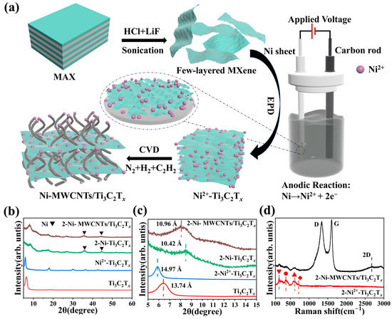
Figure 1.
(a) Schematic preparation process of Ni-MWCNTs/Ti3C2Tx. (b) XRD patterns of 2-Ni-MWCNTs/Ti3C2Tx, 2-Ni-Ti3C2Tx, Ni2+-Ti3C2Tx, and Ti3C2Tx. (c) Magnification of XRD patterns in (b,d) Raman spectra of 2-Ni-MWCNTs/Ti3C2Tx and Ni2+-Ti3C2Tx collected with a 532 nm laser. ▼ A1g(Ti, Tx), ● Eg(Tx), ▲ Eg(C), and ◆ A1g(C) represent the four characteristic peaks of Ti3C2Tx.
The XRD patterns of MAX and MXene are shown in Figure 1b. The Ti3C2Tx (104) peaks have completely disappeared, indicating that the Al layer in the MXene was completely etched. Only the (00l) peak of MXene was observed, and the main peak (002) shifted to a lower angle, indicating the successful preparation of few-layered Ti3C2Tx [34]. The Ni2+-Ti3C2Tx was vacuum-dried at 60 °C, and compared to the few-layered Ti3C2Tx, the (002) peak migrated to a lower angle. According to Bragg’s equation, the interlayer gap increases from 13.74 Å. to 14.97 Å. (Figure 1c), which suggests that Ni2+ is adsorbed in the interlayer of the few-layered Ti3C2Tx nanosheets and the opened interlayer spacing facilitates the further adsorption of Ni2+. The XRD pattern of 2-Ni-MWCNTs/Ti3C2Tx shows no peaks for Ti oxides or carbon. Compared to the 2-Ni-Ti3C2Tx with no CNT growth, its XRD (002) peak shifts to a lower angle, indicating an increase in interlayer spacing, form 10.42 Å to 10.96 Å. There are also significant shifts in the (002) peaks of 1.5-Ni-MWCNTs/Ti3C2Tx and 1-Ni-MWCNTs/Ti3C2Tx, with the peaks increasing from 10.24 Å to 10.74 Å and 10.15 Å to 10.65 Å, respectively (Figure S2). The XRD (002) peak of Ni-MWCNTs/Ti3C2Tx shifted to a lower angle as the EPD voltage increased, which may be related to the size of the Ni particles.
The Raman spectra of 2-Ni-MWCNTs/Ti3C2Tx were obtained (Figure 1d). The Raman spectra of 1.5-Ni-MWCNTs/Ti3C2Tx and 1-Ni-MWCNTs/Ti3C2Tx are shown in Figure S3. Compared to Ni2+-Ti3C2Tx, the G-band peak around 1580 cm−1, corresponding to sp2 hybridized carbon, and the D-band peak around 1330–1360 cm−1, corresponding to sp3 hybridized carbon atoms, were observed. The G-band indicates the degree of graphitization (i.e., the ordering and mass of the reactive CNTs), while the D-band reflects the degree of disorder in the carbon nanotubes. Additionally, a 2D peak near 2680 cm−1 was observed, characterizing the interlayer stacking mode or the number of layers of carbon atoms [35,36,37]. Further characterization confirmed the growth of CNTs on the surface of MXene. However, the full width at half-maximum (FWHM) of the D peak is broader and the ID /IG ratio is close to 1, indicating that the CNTs are less crystalline and more defective. This leads to a wider FWHM of the 2D peak and a less distinct peak shape. The Raman spectroscopic peaks of the 2-Ni2+-Ti3C2Tx and the 2-Ni-MWCNTs/Ti3C2Tx were identical to those of Ti3C2Tx, with a peak at 800 cm−1. The four characteristic peaks of A1g (Ti, Tx), Eg (Tx), Eg (C), and A1g (C) were observed for Ti3C2Tx [38]. Combined with the XRD date in Figure 1b, further analysis demonstrated that the chemical structure of the Ti3C2Tx matrix remained unchanged after high-temperature annealing.
The cross-sectional SEM images of 2-Ni-MWCNTs/Ti3C2Tx, 1.5-Ni-MWCNTs/Ti3C2Tx, and 1-Ni-MWCNTs/Ti3C2Tx are shown in Figure 2a–c. As expected, with CNTs acting as the bridges and Ti3C2Tx as the substrate, the in situ growth of CNTs on their interlayers and surfaces connects the Ti3C2Tx in the Z-axis direction, forming an overall conductive network [31]. From the EDS (Figure S4) of the 2-Ni-MWCNTs/Ti3C2Tx surface, the Ni element is relatively uniformly distributed, leading to the catalytic growth of high-density and uniformly distributed CNTs. From Figure 2d–f, it can be observed that there is a consistent pattern in the tube size distribution of the Ni-MWCNTs/Ti3C2Tx samples under different deposition conditions.
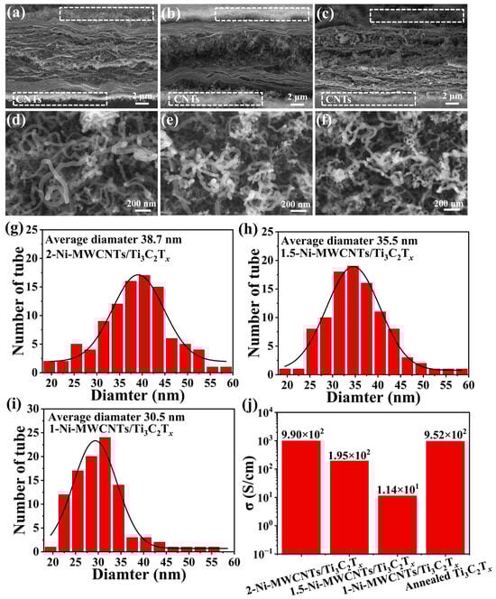
Figure 2.
SEM images of cross section from (a) 2-Ni-MWCNTs/Ti3C2Tx, (b) 1.5-Ni-MWCNTs/Ti3C2Tx, and (c) 1-Ni-MWCNTs/Ti3C2Tx. SEM images of surface from (d) 2-Ni-MWCNTs/Ti3C2Tx, (e) 1.5-Ni-MWCNTs/Ti3C2Tx, and (f) 1-Ni-MWCNTs/Ti3C2Tx. MWCNTs diameter distributions grown from (g) 2-Ni-MWCNTs/Ti3C2Tx, (h) 1.5-Ni-MWCNTs/Ti3C2Tx, and (i) 1-Ni-MWCNTs/Ti3C2Tx at 550 °C. (j) Conductivity of samples for 2-Ni-MWCNTs/Ti3C2Tx, 1.5-Ni-MWCNTs/Ti3C2Tx, 1-Ni-MWCNTs/Ti3C2Tx, and Annealed Ti3C2Tx.
In this paper, we chose to randomly measure the diameters of 100 carbon nanotubes from the surface SEM images of 2-Ni-MWCNTs/Ti3C2Tx, 1.5-Ni-MWCNTs/Ti3C2Tx, and 1-Ni-MWCNTs/Ti3C2Tx (Figures S5–S7). The results were statistically analyzed, and the range of the carbon nanotube diameters, shown in Figure 2g–i, was found to follow a normal distribution. The average tube diameters of the CNTs for 2-Ni-MWCNTs/Ti3C2Tx, 1.5-Ni-MWCNTs/Ti3C2Tx, and 1-Ni-MWCNTs/Ti3C2Tx were 38.7 nm, 35.5 nm, and 30.5 nm, respectively. The tube diameters of the CNTs increased with an increase in the voltage during the EPD, which was primarily influenced by the size of the Ni particles. The size of the catalyst particles typically determines the tube size of the CNTs, with larger catalyst particles leading to larger CNTs diameters [39]. During the electrophoretic deposition process, the concentration and ionic radius of the Ni2+ generated by Ni dissolution increased with the applied voltage [40]. As a result, the amount of Ni2+ adsorbed on the same-sized nickel sheet substrate also increased, and the aggregation of Ni2+ intensified. This led to an increase in the radius of the reduced nickel particles and the tube diameter of the grown CNTs. However, the diameter of the CNTs significantly impacts their electrical conductivity. Therefore, we characterized the electrical conductivity of 2-Ni-MWCNTs/Ti3C2Tx, 1.5-Ni-MWCNTs/Ti3C2Tx, and 1-Ni-MWCNTs/Ti3C2Tx, and found that the conductivity increased as the CNT tube diameter increased.
To further demonstrate that the size of Ni particles directly affects the tube diameter of in situ-grown CNTs in Ni-MWCNTs/Ti3C2Tx (Figures S8 and S9), TEM characterization was performed on the samples. The TEM image of 2-Ni-MWCNTs/Ti3C2Tx is shown in Figure 3a, where CNTs are clearly seen growing epitaxially from the Ti3C2Tx layers. Combined with Figure 2a and Figure S10, this confirms the in situ growth of CNTs between the Ti3C2Tx layers. Additionally, Ni particles are observed at the top of the CNTs (Figure 3b). During the catalytic growth process, CNTs form as C atoms surround the Ni particles, with sp2 hybridized C-C bonds. Therefore, the particle size directly influences the growth behavior of CNTs. Typically, smaller Ni particles generate CNTs with smaller diameters, while larger Ni particles tend to catalyze the growth of CNTs with larger diameters. For MWCNTs, the tube diameter directly affects their electrical conductivity. Larger diameters provide more electron transport channels, leading to increased conductivity [41]. Moreover, the π-π stacking effect between the walls can enhance overall conductivity by facilitating electron coupling [42]. The interlayer Ni particles of Ni-MWCNTs/Ti3C2Tx should be further characterized. The HRTEM images of 2-Ni-MWCNTs/Ti3C2Tx, 1.5-Ni-MWCNTs/Ti3C2Tx and 1-Ni-MWCNTs/Ti3C2Tx (Figure 3i–k) clearly show Ni particle lattice fringes with a spacing of 0.204 nm, corresponding to the (111) facet of fcc Ni. The particle size of Ni increases significantly with the increase in EPD voltage, which is consistent with the CNT tube diameter distribution shown in Figure 2g–i. Furthermore, the Ni particles are clearly surrounded by a few layers of graphite lattice fringes with a thickness of 0.34 nm, corresponding to the (001) crystal plane of C. In addition, the in situ-grown MWCNTs between the Ti3C2Tx layers can form a three-dimensional conductive network, enhancing electron mobility along the Z-axis and thus increasing conductivity [43]. By controlling the distribution and diameter of the MWCNTs, their electron mobility can be adjusted, thereby affecting conductivity. This is consistent with the conductivity results obtained from the experiment. As shown in Figure 2j, the conductivity of 2-Ni-MWCNTs/Ti3C2Tx, 1.5-Ni-MWCNTs/Ti3C2Tx and 1-Ni-MWCNTs/Ti3C2Tx increases with the increasing tube diameter of the CNTs, which is consistent with our prediction. However, compared to the annealed Ti3C2Tx, only 2-Ni-MWCNTs/Ti3C2Tx exhibits slightly higher conductivity. The main reason for this is that the conductivity of CNTs is not only related to their tube diameter but also influenced by their crystal structure and defects. From Figure 1d and Figure S3 Raman spectra, the ID/IG ratio of CNTs in Ni-MWCNTs/Ti3C2Tx is close to 1, indicating the presence of many defects that limit free electron transport [44], which counteracts the positive effect of the increased tube diameter. The Ni 2p pattern of 2-Ni-MWCNTs/Ti3C2Tx XPS is shown in Figure S11, the peaks at 853.6 and 870.7 eV belong to Ni0 in Ni2p3/2 and Ni2p1/2, respectively. The combination of the STEM image (Figure 3g) and the XRD pattern (Figure 1a) confirms that the Ni2+ has been successfully reduced to Ni particles. The C 1s spectra of 2-Ni-MWCNTs/Ti3C2Tx shows three peaks at 284.8, 285.6 and 286.6 eV, with distributions corresponding to C-C, C=C and C-O bonds (Figure S12) [45].
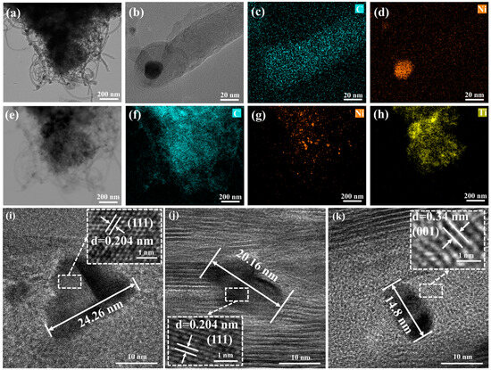
Figure 3.
TEM images of (a) 2-Ni-MWCNTs/Ti3C2Tx. (b–d) HRTEM images of CNTs/Ni and corresponding elemental mapping of C and Ni. (e–h) STEM images of 2-Ni-MWCNTs/Ti3C2Tx and corresponding elemental images of C, Ti and Ni. HRTEM images of (i) 2-Ni-MWCNTs/Ti3C2Tx, (j) 1.5-Ni-MWCNTs/Ti3C2Tx, (k) 1-Ni-MWCNTs/Ti3C2Tx.
2.2. Electromagnetic Parameter Analysis and Microwave Absorption Properties
To investigate the electromagnetic parameters of Ni-MWCNTs/Ti3C2Tx composites, the variation of the complex dielectric constant of 2-Ni-MWCNTs/Ti3C2Tx composites with different mass ratios was studied (Figure S13). The results showed that as the content of 2-Ni-MWCNTs/Ti3C2Tx increased, the complex dielectric constants (ε′ and ε″) significantly increased, while the dielectric loss tangent (tan δ) also markedly increased. This indicates that the mass ratio has a direct effect on the dielectric constant of the composite material. However, excessively high or low dielectric constants can lead to impedance mismatch between the material and free space, which is detrimental to the effective incidence of electromagnetic waves and energy dissipation [46]. Therefore, we ultimately selected 35 wt% as the filler ratio for subsequent electromagnetic parameter testing. Subsequently, we further investigated the electromagnetic parameters of composite systems with filler ratios of 35 wt% 2-Ni-MWCNTs/Ti3C2Tx, 1.5-Ni-MWCNTs/Ti3C2Tx, and 1-Ni-MWCNTs/Ti3C2Tx mixed with paraffin in the 2~18 GHz frequency range. To explore the relationship between the CNT diameter in the microstructure and the electromagnetic parameters, we analyzed the complex dielectric constant, complex permeability, dielectric loss tangent, and magnetic loss tangent of Ni-MWCNTs/Ti3C2Tx composites with different nanotube diameters. The related data are shown in Figure 4. Specifically, the average ε′ values for 2-Ni-MWCNTs/Ti3C2Tx, 1.5-Ni-MWCNTs/Ti3C2Tx, 1-Ni-MWCNTs/Ti3C2Tx and Annealed Ti3C2Tx are 17.23, 14.51, 10.46, and 16.86, respectively, while the average ε″ values are 6.15, 5.04, 2.01, and 5.64. The real part of the dielectric constant (ε′) is primarily attributed to the material’s polarization effect, while the imaginary part (ε″) is mainly associated with the material’s electrical conductivity [47]. Dielectric performance analysis shows that the 2-Ni-MWCNTs/Ti3C2Tx sample exhibits the highest real and imaginary parts of the complex dielectric constant (ε′ and ε″). This can be attributed to several synergistic effects: the wide diameter of the CNTs (38.7 nm) helps form a high-density three-dimensional conductive network, thereby improving the material’s conductivity and dielectric loss, which leads to an increase in the imaginary part of the dielectric constant. This is consistent with the trend observed in the conductivity data shown in Figure 2j. Additionally, the interface polarization (CNTs/CNTs, MXene/CNTs) and dipole polarization effects at the CNT and MXene heterojunctions further enhance the real part of the complex dielectric constant [31]. These interfacial polarization effects are closely related to the size variation of the CNTs. As the diameter of the CNTs in Ni-MWCNTs/Ti3C2Tx increases, both the real and imaginary parts of the dielectric constant increase significantly, in line with the previously discussed trends. It is noteworthy that as the CNT diameter increases, the dielectric loss tangent (tan δ) also increases (as shown in Figure 4a), which is in line with the enhanced dielectric loss capability of the material. Furthermore, due to the introduction of magnetic Ni nano-particles, the real and imaginary parts of the permeability are not at 1 and 0, respectively, but the imaginary part of the permeability was found to be negative (Figure 4b). This may be because the Ni/MWCNTs in the Ni-MWCNTs/Ti3C2Tx composites entangle with each other to form closed loops, generating eddy currents inside the composite that resist changes in the frequency of the external magnetic field in the alternating magnetic field, resulting in negative magnetic permeability [48].
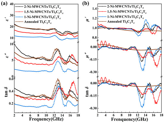
Figure 4.
(a) Complex permittivity (real part (ε′), imaginary part (ε″) and dielectric loss (tan δ = ε″/ε′) and (b) Complex permeability (real part (μ′), imaginary part (μ″) and magnetic loss (tan δ = μ″/μ′) of 2-Ni-MWCNTs/Ti3C2Tx, 1.5-Ni-MWCNTs/Ti3C2Tx, 1-Ni-MWCNTs/Ti3C2Tx, Annealed Ti3C2Tx in paraffin matrix with a loading of 35 wt%.
To evaluate the electromagnetic wave absorption characteristics of the Ni-MWCNTs/Ti3C2Tx composite system, the reflection loss (RL) of 2-Ni-MWCNTs/Ti3C2Tx, 1.5-Ni-MWCNTs/Ti3C2Tx, 1-Ni-MWCNTs/Ti3C2Tx, and annealed Ti3C2Tx was systematically studied. Based on the measured complex dielectric and magnetic permeability parameters, the reflection loss was calculated using transmission line theory and a metal backplane model, based on the measured dielectric and magnetic permeability parameters, with the calculation equation provided in the methodology section [49]. Figure 5 show the reflection loss of these materials at different thicknesses. Among these, the 2-Ni-MWCNTs/Ti3C2Tx composite shows the best reflection loss (RL) value of −44.08 dB at 7.52 GHz and a thickness of 2.49 mm, with an effective absorption bandwidth (EAB) of 1.52 GHz (8.32~6.80 GHz). This composite exhibits the best microwave absorption performance among the Ni-MWCNTs/Ti3C2Tx materials (Figure S14).
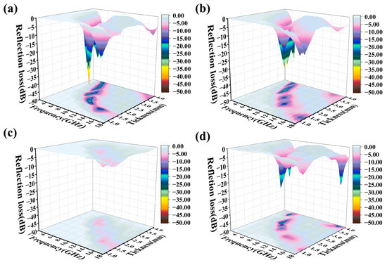
Figure 5.
3D RL of (a) 2-Ni-MWCNTs/Ti3C2Tx, (b) 1.5-Ni-MWCNTs/Ti3C2Tx, (c) 1-Ni-MWCNTs/Ti3C2Tx and (d) Annealed Ti3C2Tx versus frequency and sample thickness.
Moreover, by adjusting the thickness, the Ni-MWCNTs/Ti3C2Tx composite material can meet the electromagnetic absorption requirements across the C-band (4~8 GHz) to the X-band (8~12 GHz). This significant advantage is attributed to the synergistic regulatory effect of in situ-grown CNTs within the Ti3C2Tx layers and the CNTs with different diameters on the surface and the construction of a three-dimensional conductive network that regulates conductivity to optimize impedance matching. Meanwhile, the coupling effect between CNTs and magnetic Ni particles enhances multiple loss mechanisms. The CNT network effectively extends the electromagnetic wave transmission path, improving dielectric loss, while the Ni particles contribute to magnetic loss through eddy currents and hysteresis loss, achieving a dielectric–magnetic synergistic effect that improves impedance matching and optimizes electromagnetic wave absorption performance. In contrast, the best RL value of Annealed Ti3C2Tx is only −26.68 dB at 6.64 GHz and a thickness of 2.71 mm. The 2-Ni-MWCNTs/Ti3C2Tx and 1.5-Ni-MWCNTs/Ti3C2Tx composites, compared to Annealed Ti3C2Tx, benefit from the in situ-grown CNTs and Ni between the Ti3C2Tx layers. This combination helps increase the polarization cross-section and extend the electromagnetic wave’s loss path, while the introduction of magnetic metal particles enhances magnetic loss [50]. The synergistic effect of dielectric and magnetic conductance improves the impedance matching, thereby enhancing the absorption performance. The absorption performance of 1-Ni-MWCNTs/Ti3C2Tx is poorer, primarily due to its low dielectric loss, which results from the low dielectric imaginary part, leading to an inferior electromagnetic absorption ability. Therefore, it can be concluded that the growth and diameter of CNTs in the Ni-MWCNTs/Ti3C2Tx composite play a crucial role in determining its microwave absorption performance. Subsequently, the reflection loss–frequency curves, the relationship between simulated thickness and peak frequency, and the relationship between the input impedance ratio (Zin/Z0) and electromagnetic wave frequency of Ni-MWCNTs/Ti3C2Tx and Annealed Ti3C2Tx were investigated, as shown in Figure S15. This study found that as the absorber thickness increased, the peak reflection loss shifted to lower frequency ranges, with the best reflection loss concentrated in the C-band (4~8 GHz). This phenomenon can be explained by the quarter-wavelength equation [51,52]:
where λ is the incident wave wavelength, c is the speed of light in a vacuum, and |μr| and |εr| are the moduli of μr and εr, respectively. As the thickness decreases, the resonance frequency increases. When the thickness of the specimen is equal to a quarter of the incident electromagnetic wave’s wavelength, the electromagnetic waves reflected from the upper and lower surfaces of the specimen are in opposite phases. The interference causes the phases to cancel out, resulting in minimal absorption of the electromagnetic wave [49]. Moreover, the thicknesses corresponding to the minimum RL values in the experiment are mostly located near the tm curve, indicating that more electromagnetic waves are being absorbed.
2.3. Microwave Absorption Mechanisms
Ti3C2Tx MXene itself possesses excellent conductivity, while multiwalled carbon nanotubes (MWCNTs) form a three-dimensional conductive network through bridging interactions, further enhancing the conductivity of Ni-MWCNTs/Ti3C2Tx. This continuous 2D/2D interface (Ti3C2Tx/CNTs) provides an efficient channel for electron migration, significantly enhancing dielectric loss. The introduction of magnetic nano Ni particles modulates the charge distribution on the MXene surface, effectively alleviating the impedance mismatch problem caused by excessive conductivity [31,53]. At the same time, the Ni particles contribute to magnetic loss through eddy currents and hysteresis loss. The interface polarization effect between the CNT and MXene heterogeneous interfaces improves the impedance matching and optimizes the electromagnetic wave absorption performance. A schematic diagram of the electromagnetic wave dissipation mechanism of the Ni-MWCNTs/Ti3C2Tx is shown in Figure 6. At a frequency of around 13 GHz (Figure 4a), the ε′ of 2-Ni-MWCNTs/Ti3C2Tx shows a distinct valley, while ε″ exhibits a clear peak. Around 16 GHz, both ε′ and ε″ show peaks. This apparent fluctuation indicates the presence of substantial dielectric relaxation driven by electron motion hysteresis [54]. According to the Debye relaxation theory, the relationship between ε′ and ε″ for the material is as follows [46,55]:
where , are the static dielectric constant of the material and the dielectric constant at the ultra-high limiting frequency, respectively. According to Equation (2), the imaginary part of the dielectric constant plotted against the real part (Cole–Cole curve) will form a curve with (, 0) as the center of the circle and as the radius. The Cole–Cole plot of the Ni-MWCNTs/Ti3C2Tx and Annealed Ti3C2Tx are shown in Figure S16. The dielectric relaxation behavior of the Ni-MWCNTs/Ti3C2Tx exhibits significant synergistic effects from various loss mechanisms. In the high-frequency region, the curve shows an atypical characteristic of multiple overlapping arcs, indicating the competition and coupling of various polarization mechanisms. These mechanisms include heterogeneous interface polarization, defect dipole polarization, and dielectric–magnetic coupling of magnetic nanoparticles. Some mechanisms likely exhibit synergistic effects [56]. The rich heterogeneous interfaces and defects (such as oxygen vacancies and lattice distortion) in the Ni-MWCNTs/Ti3C2Tx are the primary sources of polarization loss [57]. The differences in electronegativity between the components lead to the accumulation of interface charges. For example, the -OH/-F groups on the surface of the Ti3C2Tx form localized electric fields with the sp2 hybridized carbon of the MWCNTs, causing a relaxation loss under alternating electromagnetic fields [58]. Additionally, the defects generated during the catalytic growth of the carbon nanotubes by Ni nanoparticles, as well as the functional groups on the MXene surface, act as dipole centers and dissipate electromagnetic energy through orientational polarization [31,59]. In the low-frequency region, the Cole–Cole curve exhibits a shape resembling a straight line with a “tail” phenomenon, indicating that conductive loss dominates. The three-dimensional conductive network formed by the MWCNTs/Ti3C2Tx directly converts electromagnetic energy into Joule heat through the migration of free charge carriers. Its unique interlayer through-structure significantly reduces surface reflectivity and extends the loss path of electromagnetic waves, achieving excellent impedance matching [43,60]. Moreover, the introduction of magnetic Ni nanoparticles enhances magnetic loss. These magnetic Ni nanoparticles are densely adsorbed and uniformly distributed within the layers and on the surface of MXene. This maximizes the effect of the magnetic nanoparticles, thereby enhancing magnetic loss and significantly improving the absorption performance of the Ni-MWCNTs/Ti3C2Tx. In contrast, the Cole–Cole curve of the Annealed Ti3C2Tx resembles a straight line, indicating the presence of only dielectric loss, with a single loss mechanism.

Figure 6.
Schematic illustration of MA mechanisms for Ni-MWCNTs/Ti3C2Tx.
3. Experimental Section
3.1. Materials
Ti3AlC2 (400 mesh, 99%) was purchased from Laizhou Kai Kai Ceramic Materials Co., Ltd. (Laizhou, China). High-purity Ni flakes (>99.96%) were purchased from Zhengchen Metal Materials Co., Ltd. (Suzhou, China). HCl was purchased from Sinopharm Chemical Reagent Co., Ltd. (99%). Hexane (>99%), HF (49 wt%) and Paraffin (>99%) was purchased from Shanghai Aladdin Biochemical Technology Co., Ltd. (Shanghai, China). All chemicals were used as received, without further purification.
3.2. Preparation of Few-Layered Ti3C2Tx MXene Suspension
The few-layered Ti3C2Tx MXene was fabricated though selective etching of the Al layer from MAX phase Ti3AlC2 powder using in situ-generated HF etchant, followed by ultrasonic exfoliation in deionized water (DI). Briefly, 2 g of LiF was stirred with 40 mL of 9 mol L−1 hydrochloric acid in a Polytetrafluoroethylene (PTFE) beaker at room temperature for 15 min. Then, 2 g of Ti3AlC2 powder was slowly added to the beaker and kept at 35 °C for 24 h. Subsequently, the suspension was washed several times with deionized water until the pH was greater than 6. The neutral solution was sonicated in an ice–water bath for 1 h to obtain as many monolayers or few layers of nanosheets as possible. Finally, the dark green solution was centrifuged at 5000 rpm for 30 min. The upper black colloidal solution was collected, and its concentration was calculated by vacuum filtration.
3.3. Preparation of Ni2+-Ti3C2Tx Membrane
The Ni2+-Ti3C2Tx MXene membrane was prepared by electrophoretic deposition (EPD) using a 1.5 × 1.5 mm nickel sheet as the working electrode, a graphite rod as the counter electrode, and an electrolyte of 3.0 mg/mL Ti3C2Tx suspension. The deposition was carried out at a constant voltage for 8 h. Subsequently, the deposited nickel sheet was put in a vacuum oven at 60 °C for 10 h. The Ni2+-Ti3C2Tx film was obtained by detaching the deposit from the nickel sheet. In this paper, constant voltages of 1 V, 1.5 V, and 2 V were applied, and the resulting Ni2+-Ti3C2Tx films were designated as 1-Ni2+-Ti3C2Tx, 1.5-Ni2+-Ti3C2Tx, and 2-Ni2+-Ti3C2Tx, respectively. The nickel flakes were ultrasonically cleaned with 1 M hydrochloric acid, ethanol, and deionized water, and then vacuum-dried at 60 °C for 4 h.
3.4. Preparation of Ni-MWCNTs/Ti3C2Tx
In situ MWCNTs were grown on surfaces and interlayers of Ti3C2Tx using low-pressure thermal chemical vapor deposition (LPTCVD). Typically, the Ni2+-Ti3C2Tx film was placed in a quartz crucible and introduced into CVD furnace. The chamber was first pumped to a pressure of less than 100 Pa at room temperature, purged with N2 for 15 min, and then heated while passing N2 and H2 at flow rates of 150 sccm and 50 sccm, respectively. The chamber was heated from room temperature to 400 °C at a rate of 5 °C/min and held at 400 °C for 30 min to allow for the reduction of nickel ions to nickel monomers. The temperature was then increased at a rate of 10 °C/min to 550 °C and held for 120 min. At 550 °C, the chamber was pumped with C2H2, and the pressure was maintained at 5 × 10⁴ Pa with a flow rate of 50 sccm. The flow rate of N2 was adjusted to 100 sccm, while the flow rate of H2 remained steady, resulting in a total gas flow rate of 200 sccm. After the holding period, C2H2 and H2 were turned off, and the chamber was cooled to room temperature in an N2 atmosphere with a flow rate of 200 sccm. The samples after in situ growth of carbon nanotubes on 1-Ni2+-Ti3C2Tx, 1.5-Ni2+-Ti3C2Tx, and 2-Ni2+-Ti3C2Tx were designated as 1-Ni-MWCNTs/Ti3C2Tx, 1.5-Ni-MWCNTs/Ti3C2Tx, and 2-Ni-MWCNTs/Ti3C2Tx, respectively. The preparation of Ni-Ti3C2Tx, compared to Ni-MWCNTs/Ti3C2Tx, involves replacing C2H2 with H2, while keeping the other LPTCVD process parameters unchanged. The preparation of Annealed Ti3C2Tx is performed using a vacuum filtration membrane for LPTCVD, with the LPTCVD process parameters being the same as those for Ni-Ti3C2Tx.
3.5. Characterization
Powder wide-angle XRD (XRD, ADVANCE D8, Bruker, Billerica, MA, USA) was performed on the samples using Cu Kα radiation (λ = 0.15406 nm) at 40 kV and 20 mA. The microstructure and composition were observed using a thermal field emission scanning electron microscope (SEM, 8230, Hitachi, Tokyo, Japan) equipped with an energy-dispersive spectroscopy (EDS) system. Transmission electron microscopy (TEM, Talos F200X, Thermo Fisher Scientific, Waltham, MA, USA) was used to identify samples’ morphology and elemental mapping. A Helios-G4-CX focused ion beam (FIB) was used to prepare the various foils. X-ray photoelectron spectroscopy (XPS, AXIS SUPRA+, SHIMADZU (CHINA) Co., Ltd., Kyoto, Japan) was performed in an XPS system with a monochromatic Al X-ray source, and the binding energy (BE) scales were assigned by adjusting the C 1s peak at 284.8 eV. Raman spectra were measured using a laser confocal Raman microscope with a He-Ne laser as an excitation line (K = 532 nm). Conductivity was measured using the AUTOMATIC FOUR POINT PROBE METER from FOUR DIMENSIONS, INC (Los Angeles, CA, USA). Electrophoretic deposition was performed using an electrochemical workstation (Bio-logic VMP3e, Seyssinet-Pariset, France) for constant voltage deposition.
The electromagnetic (EM) parameters (the complex permittivity and the complex permittivity ) of all the as-prepared samples were analyzed using an E5063A vector network analyzer. The as-prepared samples were homogeneously mixed with paraffin matrix and further pressed to form coaxial rings with an outer diameter of 7 mm and an inner diameter of 3.04 mm. According to transmission theory, the reflection loss (RL) values were calculated using the following equations [31,61]:
where , , c, d, and represent input impedance of the absorber, the characteristic impedance of free space, the velocity of light, the thickness of the absorbers, and incident EMW frequency, respectively.
4. Conclusions
In summary, Ni-MWCNTs/Ti3C2Tx composites, which in situ regulate the tube diameter of CNTs and the unique layer-by-layer structure, are prepared using the catalytic strategy of electrophoretic deposition of adsorbed metal ions, resulting in excellent wave-absorbing properties. The 2-Ni-MWCNTs/Ti3C2Tx composites exhibit the best reflection loss (RL) value of −44.08 dB and an effective absorption bandwidth of 1.52 GHz at a thickness of only 2.49 mm. The intertwined CNTs effectively connect the Z direction of the MXene, preventing the MXene from re-stacking while maintaining the high-density, uniformly dispersed Ni nanoparticles. This unusual structure reduces electromagnetic wave reflection and facilitates easier penetration of the material’s interior.
The interface polarization is enhanced by dielectric–magnetic synergy, and the magnetic loss is increased to rationally optimize the impedance matching. Additionally, the in situ modulation of the CNTs tube diameter enhances the dielectric loss of Ni-MWCNTs/Ti3C2Tx, thereby regulating the wave-absorbing properties of the composite. This approach is expected to offer a new strategy for tuning the electromagnetic wave parameters and enhancing the wave-absorbing properties of other two-dimensional materials.
Supplementary Materials
The following supporting information can be downloaded at: https://www.mdpi.com/article/10.3390/molecules30071625/s1, Figure S1: (a) XRD patterns of Ti3AlC2, Multilayered Ti3C2Tx, few-layered Ti3C2Tx. (b) Zate potential of fewlayer Ti3C2Tx MXene suspensions. Figure S2: (a) XRD patterns of 1.5-Ni-MWCNTs/Ti3C2Tx and 1.5-Ni-Ti3C2Tx. (b) XRD patterns of 1-Ni-MWCNTs/Ti3C2Tx and 1-Ni-Ti3C2Tx. Figure S3: (a) Raman spectra of 1.5-Ni-MWCNTs/Ti3C2Tx and 1.5-Ni2+-Ti3C2Tx. (b) Raman spectra of 1-Ni-MWCNTs/Ti3C2Tx and 1-Ni2+-Ti3C2Tx. Both have been collected with a 532 nm laser. ▼ A1g(Ti, Tx), ● Eg(Tx), ▲ Eg(C), and ◆ A1g(C) represent the four characteristic peaks of Ti3C2Tx. Figure S4: SEM images of (a) 2-Ni-MWCNTs/Ti3C2Tx, (b) 1.5-Ni-MWCNTs/Ti3C2Tx, (c) 1-Ni-MWCNTs/Ti3C2Tx and corresponding elemental images of Ti and Ni. Figure S5: SEM images of section 2-Ni-MWCNTs/Ti3C2Tx. Figure S6: SEM images of section 1.5-Ni-MWCNTs/Ti3C2Tx. Figure S7: SEM images of section 1-Ni-MWCNTs/Ti3C2Tx. Figure S8: TEM images of (a) 1-Ni-MWCNTs/Ti3C2Tx. (b–d) HRTEM images of CNTs/Ni and corresponding elemental mapping of C and Ni. (e–h) STEM images of 1-Ni-MWCNTs/Ti3C2Tx and corresponding elemental images of C, Ti and Ni. Figure S9: TEM images of (a) 1.5-Ni-MWCNTs/Ti3C2Tx. (b–d) HRTEM images of CNTs/Ni and corresponding elemental mapping of C and Ni. (e–h) STEM images of 1.5-Ni-MWCNTs/Ti3C2Tx and corresponding elemental images of C, Ti and Ni. Figure S10: (a) The cross-sectional TEM image of 2-Ni-MWCNTs/Ti3C2Tx. (b) TEM and (c) HRTEM images of 2-Ni-MWCNTs/Ti3C2Tx. (d–g) STEM images of 2-Ni-MWCNTs/Ti3C2Tx and corresponding elemental images of C, Ti and Ni. Figure S11: XPS spectra of Ni 2p in Ni-MWCNTs/Ti3C2Tx. Figure S12: XPS spectra of C 1s in Ni-MWCNTs/Ti3C2Tx Figure S13: Complex permittivity (real part (ε′), imaginary part (ε″) and dielectric loss (tan δ = ε″/ε′) of 2-Ni-MWCNTs/Ti3C2Tx, in paraffin matrix with different loading. Figure S14: Compared RL curves of 2-Ni-MWCNTs/Ti3C2Tx, 1.5-Ni-MWCNTs/Ti3C2Tx, 1-Ni-MWCNTs/Ti3C2Tx and Annealed Ti3C2Tx. Figure S15: RL-frequency curves, relationship between simulation thickness and peak frequency, and relationship between Zin/Z0 and electromagnetic wave frequency of (a) 2-Ni-MWCNTs/Ti3C2Tx, (b) 1.5-Ni-MWCNTs/Ti3C2Tx, (c) 1-Ni-MWCNTs/Ti3C2Tx, (d) Annealed Ti3C2Tx. Figure S16: The Cole-Cole curves of (a) 2-Ni-MWCNTs/Ti3C2Tx, (b) 1.5-Ni-MWCNTs/Ti3C2Tx, (c) 1-Ni-MWCNTs/Ti3C2Tx, (d) Annealed Ti3C2Tx.
Author Contributions
Conceptualization, Q.T., Q.F., and K.L.; methodology, Q.T., Q.F., and L.H.; software, Q.T., Q.F., Q.H.; validation, Y.C., B.F., and K.L.; formal analysis, Q.T., Q.F., P.Y., Q.H., and Y.C.; investigation, Q.T., L.H., and Q.H.; resources, K.L.; data curation, Q.T., and Q.F.; writing—original draft preparation, Q.T., and Q.F.; writing—review and editing, B.F., and K.L.; visualization, Q.H., Y.C., and B.F.; supervision, B.F., and K.L.; project administration, K.L.; funding acquisition, K.L. All authors have read and agreed to the published version of the manuscript.
Funding
This work was financially supported by the projects of Huangpu District for the STS plan of the Chinese Academy of Sciences (No. STS-HP-202309).
Institutional Review Board Statement
Not applicable.
Informed Consent Statement
Not applicable.
Data Availability Statement
Date is available at Supporting Materials.
Acknowledgments
This work gratefully acknowledges financial support from Anglo American Resources Trading (Shanghai, China) Co., Ltd.
Conflicts of Interest
The authors declare the following competing financial interests: K.L., Q.T., and Q.F. are inventors on the patent application (File No. 202411197109.9) submitted by the Ningbo Institute of Materials Technology and Engineering. Authors have received research grants from Anglo American Resources Trading (Shanghai, China) Co., Ltd. K.L., Q.T., and Q.F. are the inventor of patent (File No. 202411197109.9). The sponsors had no role in the design, execution, interpretation, or writing of the study.
References
- Iqbal, A.; Shahzad, F.; Hantanasirisakul, K.; Kim, M.K.; Kwon, J.; Hong, J.; Kim, H.; Kim, D.; Gogotsi, Y.; Koo, C.M. Anomalous absorption of electromagnetic waves by 2D transition metal carbonitride Ti3CNTx (MXene). Science 2020, 369, 446–450. [Google Scholar] [CrossRef]
- VahidMohammadi, A.; Rosen, J.; Gogotsi, Y. The world of two-dimensional carbides and nitrides (MXenes). Science 2021, 372, eabf1581. [Google Scholar] [PubMed]
- Zhang, Z.; Cai, Z.; Zhang, Y.; Peng, Y.; Wang, Z.; Xia, L.; Ma, S.; Yin, Z.; Wang, R.; Cao, Y.; et al. The recent progress of MXene-based microwave absorption materials. Carbon 2021, 174, 484–499. [Google Scholar]
- Song, L.; Zhang, F.; Chen, Y.; Guan, L.; Zhu, Y.; Chen, M.; Wang, H.; Putra, B.R.; Zhang, R.; Fan, B. Multifunctional SiC@SiO2 nanofiber aerogel with ultrabroadband electromagnetic wave absorption. Nano-Micro Lett. 2022, 14, 152. [Google Scholar]
- Gou, J.L.; Chang, Y.K.; Liu, S.; Li, P.H.; Cui, P.H.; Hu, Q.K.; Wang, L.B.; Zhang, X.; Wang, J.K.; Xia, Q.X.; et al. Solid solution strategy modulated defects engineering of (Cr1-xVx)2AlC MAX phase toward superior electromagnetic wave absorption. Rare Met. 2024, 43, 3205–3219. [Google Scholar] [CrossRef]
- Zhang, X.; Tian, X.L.; Qin, Y.; Qiao, J.; Pan, F.; Wu, N.; Wang, C.; Zhao, S.; Liu, W.; Cui, J.; et al. Conductive metal-organic frameworks with tunable dielectric properties for boosting electromagnetic wave absorption. ACS Nano 2023, 17, 12510–12518. [Google Scholar] [CrossRef] [PubMed]
- Wang, G.; Li, C.; Estevez, D.; Xu, P.; Peng, M.; Wei, H.; Qin, F. Boosting interfacial polarization through heterointerface engineering in MXene/Graphene intercalated-based microspheres for electromagnetic wave absorption. Nano-Micro Lett. 2023, 15, 152. [Google Scholar]
- Zou, Z.; Ning, M.; Lei, Z.; Zhuang, X.; Tan, G.; Hou, J.; Xu, H.; Man, Q.; Li, J.; Li, R.W. 0D/1D/2D architectural Co@C/MXene composite for boosting microwave attenuation performance in 2~18 GHz. Carbon 2022, 193, 182–194. [Google Scholar] [CrossRef]
- Su, X.; Wang, J.; Zhang, X.; Huo, S.; Dai, W.; Zhang, B. Synergistic effect of polyhedral iron-cobalt alloys and graphite nanosheets with excellent microwave absorption performance. J. Alloys Compd. 2020, 829, 154426. [Google Scholar] [CrossRef]
- Zhuang, X.; Tan, G.; Ning, M.; Qi, C.; Ge, X.; Yang, Z.; Man, Q. Boosted microwave absorbing performance of Ce2Fe17N3-δ@SiO2 composite with broad bandwidth and low thickness. J. Alloys Compd. 2021, 883, 160835. [Google Scholar]
- Iqbal, A.; Sambyal, P.; Koo, C.M. 2D MXenes for electromagnetic shielding: A Review. Adv. Funct. Mater. 2020, 30, 2000883. [Google Scholar]
- Lei, Z.; Zhu, S.; Sun, X.; Yu, S.; Liu, X.; Liang, K.; Zhang, X.; Qu, L.; Wang, L.; Zhang, X. A multiscale porous 3D-Fabric evaporator with vertically aligned yarns enables ultra-efficient and continuous water desalination. Adv. Funct. Mater. 2022, 32, 2205790. [Google Scholar]
- Zhang, J.; Liu, Y.; Liao, Z.; Hu, J.; Ma, A.; Ma, Y.; Feng, C.; Ma, M. MoS2-based materials for microwave absorption: An overview of recent advances and prospects. Synth. Met. 2022, 291, 117188. [Google Scholar]
- Nie, Z.; Feng, Y.; Hu, X.; Su, J.; Zhao, Z.; Chen, J.; Wang, R.; Qi, S. In situ-growth ultrathin hexagonal boron nitride/N-doped reduced graphene oxide composite aerogel for high performance of thermal insulation and electromagnetic wave absorption. Ceram. Int. 2023, 49, 36080–36091. [Google Scholar]
- Wang, F.; Bai, C.; Chen, L.; Yu, Y. Boron nitride nanocomposites for microwave absorption: A review. Mater. Today Nano. 2021, 13, 100108. [Google Scholar]
- Shahzad, F.; Alhabeb, M.; Hatter, C.B.; Anasori, B.; Man Hong, S.; Koo, C.M.; Gogotsi, Y. Electromagnetic interference shielding with 2D transition metal carbides (MXenes). Science 2016, 353, 1137–1140. [Google Scholar]
- Song, Q.; Ye, F.; Kong, L.; Shen, Q.; Han, L.; Feng, L.; Yu, G.; Pan, Y.; Li, H. Graphene and MXene nanomaterials: Toward high-performance electromagnetic wave absorption in gigahertz band range. Adv. Funct. Mater. 2020, 30, 2000475. [Google Scholar]
- Hart, J.L.; Hantanasirisakul, K.; Lang, A.C.; Anasori, B.; Pinto, D.; Pivak, Y.; van Omme, J.T.; May, S.J.; Gogotsi, Y.; Taheri, M.L. Control of MXenes’ electronic properties through termination and intercalation. Nat. Commun. 2019, 10, 522. [Google Scholar]
- Sun, B.; Wang, N.; Xie, X.; Zhong, L.; He, L.; Xiang, M.; Liang, K.; Hu, W. Flexible aqueous Cr-Ion hybrid supercapacitors with remarkable electrochemical properties in all climates. Angew. Chem. Int. Ed. 2024, 63, e202408569. [Google Scholar]
- He, L.; Zhuang, H.; Fan, Q.; Yu, P.; Wang, S.; Pang, Y.; Chen, K.; Liang, K. Advances and challenges in MXene-based electrocatalysts: Unlocking the potential for sustainable energy conversion. Mater. Horiz. 2024, 11, 4239–4255. [Google Scholar]
- Li, Z.Y.; Zhao, W.J.; Sun, Y.; Zhou, B.; Feng, Y.Z.; Liu, C.T. Comparative enhancement of H+ and OH− treatment on electromagnetic interference shielding in aligned and compact Ti3C2Tx MXene film. Rare Met. 2025, 44, 1833–1843. [Google Scholar]
- Li, X.; Wang, G.; Li, Q.; Wang, Y.; Lu, X. Dual optimized Ti3C2Tx MXene@ZnIn2S4 heterostructure based on interface and vacancy engineering for improving electromagnetic absorption. Chem. Eng. J. 2023, 453, 139488. [Google Scholar]
- Sun, C.; Jia, Z.; Xu, S.; Hu, D.; Zhang, C.; Wu, G. Synergistic regulation of dielectric-magnetic dual-loss and triple heterointerface polarization via magnetic MXene for high-performance electromagnetic wave absorption. J. Mater.Sci. Technol. 2022, 113, 128–137. [Google Scholar]
- Li, Y.; Meng, F.; Mei, Y.; Wang, H.; Guo, Y.; Wang, Y.; Peng, F.; Huang, F.; Zhou, Z. Electrospun generation of Ti3C2Tx MXene@graphene oxide hybrid aerogel microspheres for tunable high-performance microwave absorption. Chem. Eng. J. 2020, 391, 123512. [Google Scholar]
- Wang, J.; Wu, Z.; Xing, Y.; Li, B.; Huang, P.; Liu, L. Multi-Scale design of Ultra-Broadband microwave metamaterial absorber based on hollow Carbon/MXene/Mo2C microtube. Small 2023, 19, 2207051. [Google Scholar]
- Cui, Y.; Yang, K.; Wang, J.; Shah, T.; Zhang, Q.; Zhang, B. Preparation of pleated RGO/MXene/Fe3O4 microsphere and its absorption properties for electromagnetic wave. Carbon 2021, 172, 1–14. [Google Scholar]
- Kong, L.; Zhang, G.; Cui, H.; Qi, J.; Wang, T.; Xu, H. Deformation induced absorption band-tunable smart CNTs/Ti3C2Tx-WPU electromagnetic wave absorbing aerogel. Carbon 2024, 223, 119023. [Google Scholar]
- Tao, W.; Shao, W.; Ma, M.; Chen, S.; Shi, Y.; He, H.; Zhu, Y.; Wang, X. Ag anchored mesoporous carbon hollow sphere in Cellulose nanofibers/MXene composite films for high-performance electromagnetic interference shielding. Nano Mater. Sci. 2024, 6, 2589–9651. [Google Scholar]
- Chen, L.; Pan, J.; Wang, T.; Xia, W.; He, J.; Zhang, K. 1D Magnetic nickel-carbon matrix nanotube composites derived from Hydrogen-Bonded organic frameworks and metal-organic frameworks for electromagnetic wave absorption. Adv. Funct. Mater. 2025, 35, 2409432. [Google Scholar] [CrossRef]
- Huynh, T.M.; Nguyen, S.; Nguyen, N.T.; Nguyen, H.M.; Do, N.U.; Nguyen, D.C.; Nguyen, L.H.; Nguyen, C.V. Effects of catalyst pretreatment on carbon nanotube synthesis from methane using thin stainless-steel foil as catalyst by chemical vapor deposition method. Nanomaterials 2021, 11, 50. [Google Scholar]
- Li, X.; You, W.; Xu, C.; Wang, L.; Yang, L.; Li, Y.; Che, R. 3D seed-germination-like MXene with In Situ Growing CNTs/Ni Heterojunction for Enhanced Microwave Absorption via Polarization and Magnetization. Nano-Micro Lett. 2021, 13, 157. [Google Scholar] [CrossRef]
- Zheng, C.; Yao, Y.; Rui, X.; Feng, Y.; Yang, D.; Pan, H.; Yu, Y. Functional MXene-based Materials for next-generation rechargeable batteries. Adv. Mater. 2022, 34, 2204988. [Google Scholar] [CrossRef] [PubMed]
- Luo, Y.; Que, W.; Tang, Y.; Kang, Y.; Bin, X.; Wu, Z.; Yuliarto, B.; Gao, B.; Henzie, J.; Yamauchi, Y. Regulating functional groups enhances the performance of flexible microporous MXene/Bacterial cellulose electrodes in supercapacitors. ACS Nano 2024, 18, 11675–11687. [Google Scholar] [CrossRef]
- Naguib, M.; Unocic, R.R.; Armstrong, B.L.; Nanda, J. Large-scale delamination of multi-layers transition metal carbides and carbonitrides “MXenes”. Dalton Trans. 2015, 44, 9353–9358. [Google Scholar] [CrossRef] [PubMed]
- Baghel, P.; Kaushal, P. Rapid synthesis of carbon nanotubes from Prosopis juliflora biochar using microwave irradiation. Mater. Sci. Eng. B 2022, 286, 115987. [Google Scholar] [CrossRef]
- Gogotsi, Y.; Libera, J.A.; Kalashnikov, N.; Yoshimura, M. Graphite polyhedral crystals. Science 2000, 290, 317–320. [Google Scholar] [CrossRef]
- Rao, A.M.; Richter, E.; Bandow, S.; Chase, B.; Eklund, P.C.; Williams, K.A.; Fang, S.; Subbaswamy, K.R.; Menon, M.; Thess, A.; et al. Diameter-Selective Raman scattering from vibrational modes in carbon nanotubes. Science 1997, 275, 187–191. [Google Scholar] [CrossRef] [PubMed]
- Shevchuk, K.; Sarycheva, A.; Shuck, C.E.; Gogotsi, Y. Raman spectroscopy characterization of 2D carbide and carbonitride MXenes. Chem. Mater. 2023, 35, 8239–8247. [Google Scholar] [CrossRef]
- Zhang, R.; Zhang, Y.; Wei, F. Horizontally aligned carbon nanotube arrays: Growth mechanism, controlled synthesis, characterization, properties and applications. Chem. Soc. Rev. 2017, 46, 3661–3715. [Google Scholar]
- Liu, W.; Ding, X.; Cheng, J.; Jing, J.; Li, T.; Huang, X.; Xie, P.; Lin, X.; Ding, H.; Kuang, Y.; et al. Inhibiting dissolution of active sites in 80 °C alkaline water electrolysis by oxyanion engineering. Angew. Chem. Int. Ed. 2024, 63, e202406082. [Google Scholar] [CrossRef]
- Chen, G.; Futaba, D.N.; Sakurai, S.; Yumura, M.; Hata, K. Interplay of wall number and diameter on the electrical conductivity of carbon nanotube thin films. Carbon 2014, 67, 318–325. [Google Scholar] [CrossRef]
- Zhou, Y.; Fang, Y.; Ramasamy, R.P. Non-Covalent functionalization of carbon nanotubes for electrochemical biosensor development. Sensors 2019, 19, 392. [Google Scholar] [CrossRef] [PubMed]
- Weng, C.; He, J.; Tian, J.; Wu, W.; Li, J.; Zhang, J.; Yu, H.; Zhang, X.; Lu, M. Ultrathin MWCNT/Ti3C2Tx hybrid films for electromagnetic interference shielding. Nanomaterials 2025, 15, 6. [Google Scholar] [CrossRef]
- Zhao, Y.; Wang, J.; Yang, D.; Du, Z.; Zhi, X.; Yu, R.; Guo, Z.; Tang, C.; Fang, Y. MXene-CNTs/Co dielectric-electromagnetic synergistic composites with multi-heterogeneous interfaces for microwave absorption. Carbon 2025, 232, 119825. [Google Scholar] [CrossRef]
- Wang, H.Y.; Sun, X.-B.; Yang, S.H.; Zhao, P.Y.; Zhang, X.J.; Wang, G.S.; Huang, Y. 3D ultralight hollow NiCo compound@MXene composites for tunable and high-efficient microwave absorption. Nano-Micro Lett. 2021, 13, 206. [Google Scholar] [CrossRef]
- Niu, H.; Jiang, X.; Li, W.; Min, Z.; Putra, B.R.; Wahyuni, W.T.; Wang, H.; Zhang, R.; Fan, B. Enhanced electromagnetic wave absorption via optical fiber-like PMMA@Ti3C2Tx@SiO2 composites with improved impedance matching. Nano Res. 2024, 17, 1676–1686. [Google Scholar] [CrossRef]
- Lv, H.; Ji, G.; Liang, X.; Zhang, H.; Du, Y. A novel rod-like MnO2@Fe loading on graphene giving excellent electromagnetic absorption properties. J. Mater. Chem. C 2015, 3, 5056–5064. [Google Scholar] [CrossRef]
- Yao, X.; Kou, X.; Qiu, J. Multi-walled carbon nanotubes/polyaniline composites with negative permittivity and negative permeability. Carbon 2016, 107, 261–267. [Google Scholar] [CrossRef]
- Chang, M.; Li, Q.; Jia, Z.; Zhao, W.; Wu, G. Tuning microwave absorption properties of Ti3C2Tx MXene-based materials: Component optimization and structure modulation. J. Mater. Sci. Technol. 2023, 148, 150–170. [Google Scholar] [CrossRef]
- Li, X.; Wu, Z.; You, W.; Yang, L.; Che, R. Self-Assembly MXene-rGO/CoNi film with massive continuous heterointerfaces and enhanced magnetic coupling for superior microwave absorber. Nano-Micro Lett. 2022, 14, 73. [Google Scholar] [CrossRef]
- Cao, M.S.; Cai, Y.Z.; He, P.; Shu, J.C.; Cao, W.Q.; Yuan, J. 2D MXenes: Electromagnetic property for microwave absorption and electromagnetic interference shielding. Chem. Eng. J. 2019, 359, 1265–1302. [Google Scholar]
- Jiang, X.; Wang, Q.; Song, L.; Lu, H.; Xu, H.; Shao, G.; Wang, H.; Zhang, R.; Wang, C.; Fan, B. Enhancing electromagnetic wave absorption with core-shell structured SiO2@MXene@MoS2 nanospheres. Carbon Energy 2024, 6, e502. [Google Scholar] [CrossRef]
- Zhou, Y.; Zhang, W.; Pan, D.; Li, Z.; Zhou, B.; Huang, M.; Mi, L.; Liu, C.; Feng, Y.; Shen, C. Absorption-Reflection-Transmission power coefficient guiding gradient distribution of magnetic MXene in layered composites for electromagnetic wave absorption. Nano-Micro Lett. 2025, 17, 147. [Google Scholar]
- Li, M.; Han, M.; Zhou, J.; Deng, Q.; Zhou, X.; Xue, J.; Du, S.; Yin, X.; Huang, Q. Novel scale-like structures of Graphite/TiC/Ti3C2 hybrids for electromagnetic absorption. Adv. Electron. Mater. 2018, 4, 1700617. [Google Scholar] [CrossRef]
- Gao, C.; Zhang, H.; Zhang, D.; Gao, F.; Liu, Y.; Chen, X.; Wu, D.; Terrones, M.; Wang, Y. Sustainable synthesis of tunable 2D porous carbon nanosheets toward remarkable electromagnetic wave absorption performance. Chem. Eng. J. 2023, 476, 146912. [Google Scholar]
- Zhou, Z.; Zhu, Q.; Liu, Y.; Zhang, Y.; Jia, Z.; Wu, G. Construction of self-assembly based tunable absorber: Lightweight, hydrophobic and self-cleaning properties. Nano-Micro Lett. 2023, 15, 137. [Google Scholar]
- Zhou, X.; Wen, J.; Wang, Z.; Ma, X.; Wu, H. Broadband high-performance microwave absorption of the single-layer Ti3C2Tx MXene. J. Mater. Sci. Technol. 2022, 115, 148–155. [Google Scholar]
- Wang, W.; Ding, X.; Lin, D.; Feng, Y.; Fu, H.; Liu, C.; Tian, K.; Xu, P.; Li, Q. Manipulating highly ordered MXene porous composites by directional freezing for absorption effectiveness-enhanced electromagnetic interference shielding. ACS Appl. Nano Mater. 2024, 7, 28582–28592. [Google Scholar]
- Liu, X.; Zhou, J.; Xue, Y.; Lu, X. Structural engineering of hierarchical magnetic/carbon nanocomposites via in situ growth for high-efficient electromagnetic wave absorption. Nano-Micro Lett. 2024, 16, 174. [Google Scholar] [CrossRef] [PubMed]
- Yan, H.; Guo, Y.; Bai, X.; Qi, J.; Lu, H. Facile constructing Ti3C2Tx/TiO2@C heterostructures for excellent microwave absorption properties. J. Colloid. Interface Sci. 2024, 654, 1483–1491. [Google Scholar]
- Wang, J.; Zhang, L.; Yan, J.; Yun, J.; Zhao, W.; Dai, K.; Wang, H.; Sun, Y. MXene-based ultrathin electromagnetic wave absorber with hydrophobicity, anticorrosion, and quantitively classified electrical losses by intercalation growth nucleation engineering. Adv. Funct. Mater. 2024, 34, 2402419. [Google Scholar]
Disclaimer/Publisher’s Note: The statements, opinions and data contained in all publications are solely those of the individual author(s) and contributor(s) and not of MDPI and/or the editor(s). MDPI and/or the editor(s) disclaim responsibility for any injury to people or property resulting from any ideas, methods, instructions or products referred to in the content. |
© 2025 by the authors. Licensee MDPI, Basel, Switzerland. This article is an open access article distributed under the terms and conditions of the Creative Commons Attribution (CC BY) license (https://creativecommons.org/licenses/by/4.0/).