1. Introduction
Perovskite solar cells (PSCs) have emerged as a prominent photovoltaic technology in recent years owing to their exceptional optoelectronic properties, including high absorption coefficients, superior charge carrier mobility, extended diffusion lengths, and tunable bandgaps [
1,
2,
3]. Remarkable progress has been evidenced by the dramatic efficiency enhancement from an initial 3.8% to a current certified record of 26.7%, underscoring their commercial viability. Solution processing remains the predominant fabrication approach for PSCs due to its simplicity and scalability. Conventional one-step solution methods typically employ organic solvents such as dimethyl sulfoxide (DMSO) [
4], N,N-dimethylformamide (DMF) [
5], N-methylpyrrolidone (NMP) [
6], and γ-butyrolactone (GBL) [
7] to dissolve organic ammonium salts and metal halides. Anti-solvents, including chlorobenzene (CB), toluene (Tol), and diethyl ether (DEE), are subsequently utilized to enhance film quality. However, these solvents pose significant health risks, particularly to hepatic, respiratory, and neurological systems [
8], leading to stringent regulatory restrictions in various countries.
While alternative solvents with reduced toxicity, such as ethyl acetate, triethyl phosphate, methylammonium formate, and potassium ammonium acetate, have been explored as green alternatives [
9,
10], their large-scale industrial application remains problematic. From an environmental perspective, water represents an ideal solvent candidate, offering both cost-effectiveness and non-toxicity. Nevertheless, challenges persist due to the limited solubility of lead halides in aqueous systems and the inherent susceptibility of perovskite films to moisture-induced degradation [
11].
The pioneering work by Wei et al. demonstrated the feasibility of aqueous-based PSC fabrication using Pb(NO
3)
2 precursors through the sequential deposition method, achieving a relatively low power conversion efficiency (PCE) of 12.58% [
12]. Despite this advancement, the conversion kinetics from Pb(NO
3)
2 to perovskite remains sluggish [
13,
14,
15], compounded by the detrimental effects of nitrate ions on newly formed metastable perovskite [
16]. Recent efforts have focused on enhancing the conversion efficiency of Pb(NO
3)
2 and mitigating the degradation of perovskite, including: (1) Process optimization: Muhammad Adnan developed a multi-soaking annealing protocol to improve Pb(NO
3)
2 conversion and film quality. (2) Deposition techniques: Yue Feng demonstrated enhanced conversion rates through multiple drop-casting approaches [
17]. (3) Crystallinity control: Zhai et al. achieved pinhole-free, large-grain films via dry air and oleate anion-mediated crystallization [
18]. (4) Nucleation engineering: Nano-seed fluids have been employed to reduce nucleation barriers and refine grain structures [
19]. (5) Photon-assisted synthesis: Light irradiation has been utilized to modulate the PbI
2 microstructure and facilitate lead chloride conversion [
20]. These advancements have propelled the PCE of aqueous-processed PSCs to 24%, comparable to the performance of organic solvent-based counterparts.
Previous research on high-performance PSCs utilizing aqueous Pb(NO
3)
2 precursors has predominantly focused on mesoporous TiO
2-based regular (n-i-p) architectures. However, these configurations present several limitations: (1) the necessity for high-temperature sintering of mesoporous materials increases energy consumption and fabrication complexity, and (2) the reliance on costly spiro-OMeTAD as the hole transport layer. In contrast, planar inverted (p-i-n) PSCs offer distinct advantages, including low-temperature processing compatibility, enhanced flexibility, cost-effectiveness, and simplified fabrication procedures [
21]. Despite these benefits, planar inverted PSCs fabricated from aqueous Pb(NO
3)
2 precursors have demonstrated limited efficiencies, reaching only 6.46% [
22].
The fundamental challenge in Pb(NO
3)
2-based perovskite formation lies in the complex transformation mechanism, which involves MAX solution infiltration and substantial volume changes. Particularly noteworthy is the approximately two-fold volumetric expansion during the PbI
2-to-perovskite conversion [
23]. This transformation process leads to surface pore blockage in the Pb(NO
3)
2 layer, impeding MAX solution infiltration and hindering the conversion of underlying Pb(NO
3)
2 and PbI
2. Furthermore, the inherently slow conversion kinetics in the Pb(NO
3)
2/H
2O system exacerbates these issues through Ostwald ripening effects [
20], which promote crystal growth at the expense of smaller particles, thereby intensifying the pore clogging phenomenon.
To address these challenges, strategic enlargement of the Pb(NO
3)
2 film’s pore structure emerges as a promising solution. This approach facilitates deeper MAX solution penetration, mirroring the successful implementation of porous architectures in regular PSCs that have enabled high efficiencies in aqueous Pb(NO
3)
2-based systems. Addressing the incomplete conversion issue in aqueous Pb(NO
3)
2-based planar perovskite films remains an urgent challenge. In this study, we employ sodium dodecyl sulfonate (SDS) as a surfactant additive, building upon previous literature reports [
24,
25], to systematically investigate its impact on the Pb(NO
3)
2-to-perovskite transformation. Our experimental results reveal that SDS modification significantly enhances the conversion process through multiple mechanisms: (1) modification of the Pb(NO
3)
2 film surface properties, (2) accelerated MAX solution diffusion and subsequent Pb(NO
3)
2 conversion, and (3) improved energy level alignment between the hole transport layer and perovskite.
The incorporation of SDS enables the fabrication of uniform, dense perovskite films with reduced structural defects. Notably, the sulfonic acid groups in SDS effectively coordinate with under-coordinated Pb2+ ions, leading to substantial suppression of non-radiative recombination. Furthermore, the SDS-modified devices demonstrate enhanced charge carrier extraction and reduced lattice strain during the conversion process. These synergistic effects result in a remarkable improvement in device performance, with champion planar inverted PSCs achieving a power conversion efficiency of 14.82%—a significant enhancement compared to the 12.27% efficiency of reference devices without SDS additive.
2. Results and Discussion
Figure S1 shows a molecular structure diagram of SDS, and
Figure S2 presents the schematic flowchart of the preparation of perovskite films from Pb(NO
3)
2 with and without SDS doping. As indicated in the flowchart, different concentrations of SDS aqueous solutions were added into the Pb(NO
3)
2 solution to finally form mixed solutions with a concentration of 1.8 M of Pb(NO
3)
2 and different concentrations (0, 1 × 10
−2, 1.6 × 10
−5, 6.4 × 10
−7 mg·mL
−1) of SDS. Then, their impacts on the device performance were investigated by evaluating the performance of the PSC devices. The PSCs were obtained by a two-step method: a Pb(NO
3)
2 film was prepared by spin coating aqueous Pb(NO
3)
2 precursor solution, and then perovskite was slowly formed in an organic mixed halide (MAX) solution containing MACl and MAI. By comparing the perovskite film without SDS (control device), 1.6 × 10
−5 mg·mL
−1 was found out to be the optimal doping concentration.
According to literature reports, the conversion from Pb(NO
3)
2 to perovskite film can be divided into two sequential steps: Pb(NO
3)
2 first reacts rapidly with MAX to generate PbI
2, and then PbI
2 slowly converts into perovskite within hundreds of seconds.
The slow transformation in the latter stage easily induces the well-known Ostwald ripening effect, and volume expansion occurs during the conversion from PbI
2 to perovskite. Therefore, the state of the Pb(NO
3)
2 film directly affects the infiltration of the MAX solution and the conversion rate. As SEM shows in
Figure 1a–d, Pb(NO
3)
2 films treated with SDS do show some morphology changes. The estimations of pore sizes of the Pb(NO
3)
2 films are shown in
Figure 1e–h, demonstrating the largest pore size at the SDS doping concentration of 1.6 × 10
−5 mg·mL
−1. The enlarged pores size of the Pb(NO
3)
2 film help to infiltrate more MAX to conduct reactions (1) and (2). This enlarged pore size of Pb(NO
3)
2 film is partially supported by the slightly enhanced absorbance measurements of the Pb(NO
3)
2 film after SDS doping due to larger scattering, as UV-Vis spectra of Pb(NO
3)
2 film shown in
Figure S3. However, the addition of excessive concentrations will hinder the formation of the porous Pb(NO
3)
2 film. Apparently, SDS promotes the nucleation and growth rate of perovskite by increasing the pores of Pb(NO
3)
2 film. Firstly, when Pb(NO
3)
2 infiltrates into the MAX solution, perovskite is rapidly formed on its surface through reactions (1) and (2). Some studies have also reported that the newly formed perovskite is in a metastable state and is easily affected by NO
3−. Due to the smaller pores of the control sample, a large amount of NO
3− is trapped in the MAPbI
3 lattice due to its slowed diffusion. NO
3− can combine with MA
+ to cause the collapse of the metastable perovskite structure, which destroys most of the metastable perovskite. Prolonged incubation in MAX solution will gradually accumulate stable perovskite. Thus, the accumulation of stable perovskite will be pronounced for the sample with suitable pore sizes. To further verify this inference, we used a digital camera to take real-time photos to record the dynamic conversion process from Pb(NO
3)
2 to perovskite during the experiments, as shown in
Figure 1i. Initially, the surface color of Pb(NO
3)
2 is almost the same before immersion in MAX solution. After 120 s of immersion, the surface of the control sample turns yellow, which can be understood as a large amount of Pb(NO
3)
2 being converted into PbI
2, while the SDS-treated sample appears brown, a mixture of black and yellow. This can be explained as the generation of a large amount of perovskite in addition to PbI
2. In four minutes, both samples turn black with the faster color change of the SDS-doped sample.
The conversion process inferred from the digital photos can be verified by XRD measurements. As shown in
Figure 1j,k, both control and the SDS-treated groups show the characteristic diffraction peaks of Pb(NO
3)
2 initially. After 120 s immersion in MAX solution, PbI
2 is detected at 12.64° in both groups with a weak perovskite peak at 14.27° in the SDS-treated group, indicating that the reaction rate between Pb(NO
3)
2 and MAX is accelerated by SDS treatment. Further immersion in MAX solution gradually decreases PbI
2 and increases perovskite in both groups.
Figure 1l calculates the proportion of MAPbI
3 generated in each group based on the peak intensity of perovskite and the sum of perovskite and PbI
2. According to the calculation results, the forming of perovskite in the SDS-treated group is faster and the proportion of MAPbI
3 is always greater than that in the control group, confirming the phenomenon shown in
Figure 1i.
Long-alkyl-chain surfactants are regarded as effective additives for altering the rheological properties of inks and improving the quality of perovskite film. Theoretically, low interfacial free energy is more conducive to liquid infiltration. SDS consists of a long hydrocarbon compound with a sulfonic acid functional group and a small inorganic cation (Na
+), having a passivating effect both at grain boundaries and on crystal planes [
26]. The electrostatic potential distribution is shown in
Figure S4. As FTIR shows in
Figure S5, the characteristic stretching vibration peak of SDS was detected at around 2900 cm
−1 after doping SDS with Pb(NO
3)
2, and the position of SO
3- shifted from the original 1127 to 1150 cm
−1, indicating the existence of SDS and its interaction with Pb(NO
3)
2.
In this paper, the influence of surfactants on crystal nucleation was discussed based on the classical thermodynamic theory [
27]. The nucleation rate
V1 can be expressed as:
In the formula,
k is a constant,
KB is the Boltzmann constant,
T is the absolute temperature,
A is a complex function of the molecular-level diffusion kinetic parameters, and
ΔG* is the critical free energy of nucleation. Heterogeneous nucleation sites are limited by the available surface area of substrates and colloidal particles in the precursor solution. The relationship between homogeneous and heterogeneous nucleation is expressed as:
where
According to the test results of the static contact angle in
Figure 2a,d,
θ decreases from 39.07° to 31.09° to lower the energy barrier required for nucleation, as shown in
Figure 2g. The nucleation rate is thus accelerated by the reduced barrier.
Figure 2b,e display the surface roughness measured by atomic force microscopy. The average surface roughness of the Pb(NO
3)
2 film increased from 36.4 to 42.5 nm after SDS doping. The increased surface roughness can be attributed to the formation of additional nucleation sites, which can facilitate the growth of high-quality perovskite films on the substrate [
28,
29].
To investigate the impact of SDS treatment on perovskite film morphology, SEM characterizations on the cross-sections of Pb(NO
3)
2 films and the surfaces/cross-sections of perovskite films were conducted. Compared to the control sample without SDS doping (
Figure 3a), the cross-section of Pb(NO
3)
2 film after SDS doping exhibits closer contact with the bottom interface (
Figure 3b). Control perovskite films exhibit rugged surfaces with base pore defects due to incomplete precursor conversion, where a surface perovskite layer obstructs MAX infiltration, leaving unreacted Pb(NO
3)
2. In contrast, SDS-treated films feature enlarged Pb(NO
3)
2 pores, enabling deeper MAX penetration and more thorough conversion, yielding uniform, compact morphologies. Control films also show granular crystals from volume expansion stress and unstable decomposition products (e.g., PbI
2) [
30,
31], which induce electrical shunting and recombination [
32]. SDS treatment reduces these defects by increasing nucleation sites and pore roughness, promoting larger, denser crystals. AFM (
Figure 3g,h) confirms smoother SDS-treated surfaces (RMS: 36.2 nm vs. 42.4 nm), enhancing contact with subsequent layers such as PC
61BM for better carrier extraction. Additionally, SDS lowers the precursor solution’s contact angle (5.13° vs. 7.65°, as shown in
Figure S6), improving wettability. The lower contact angle means smaller surface energy, which is conducive to the infiltration and crystallization of perovskite [
33]. Grazing-incidence XRD can reveal residual stress in films from lattice expansion. As shown in
Figure 3i,j, as the incident angle increases, the diffraction peaks of the samples in the control group shift to lower angles, indicating tensile stress due to lattice expansion [
34]. However, SDS-treated films exhibit negligible stress due to accelerated conversion kinetics, yielding high-quality perovskite layers with minimized structural imperfections.
UPS was employed to characterize the perovskite films of the control and SDS-treated groups, aiming to investigate the effect of SDS incorporation on interfacial hole extraction. As shown in
Figure 4a,d, the low-energy electron
cut-off edges of the control and SDS-treated perovskite films are located at
16.19 and
17.15 eV, respectively. According to the formula E
F = 21.22 − E
cut-off, the Fermi levels of the control and SDS-treated perovskite films are calculated to be
5.03 and
4.07 eV, respectively. As depicted in
Figure 4b,e the Fermi edges of the control and SDS-treated groups are located at
0.9 and
1.71 eV, respectively. Based on the formula E
VB = E
F − E
F, edge, the valence band energy levels (E
VB) of the control and SDS-treated groups are calculated to be
5.93 and
5.78 eV, respectively. To further analyze the energy level parameters, the optical absorption spectra of both films were characterized by UV-Vis spectroscopy. As shown in
Figure 4c and S4, the optical bandgaps are both calculated to be
1.603 eV. Using these data, the conduction band energy levels (E
CB) of the control and SDS-treated films are derived to be
4.327 and
4.177 eV, respectively. Finally, the energy level alignment diagram is summarized in
Figure 4f Compared with the control group, the minimum of the conduction band in the SDS-treated perovskite film is closer to that of the PEDOT:PSS film. This reduced energy offset facilitates hole extraction from the perovskite to PEDOT:PSS, thereby minimizing open-circuit voltage (V
OC) losses. Additionally, the low energy barrier between the perovskite and PC
61BM enhances electron injection efficiency. The synergistic improvement in hole extraction and electron injection efficiency after SDS modification contributes to an increased fill factor (FF) of the device.
Defect states significantly influence carrier recombination in PSCs. To investigate interfacial carrier dynamics, TPC and TPV measurements were performed. As shown in
Figure 5a,b the TPC decay time of the SDS-treated device (
0.762 µs) is shorter than that of the control group (
0.997 µs), indicating enhanced charge extraction efficiency. Conversely, the TPV decay time of the SDS-treated device (
4.689 µs) is longer than that of the control group (
0.125 µs), suggesting reduced interfacial defects and suppressed non-radiative recombination. As shown in
Figure 5c, Mott–Schottky measurements reveal that the flat-band potential (V
bi) of the SDS-treated device increases by
0.025 V compared to the control group, which directly contributes to the improved V
OC. A higher V
bi enhances the driving force for charge separation and extraction [
35]. The Nyquist plots of the devices in the control and the SDS-treated groups measured by EIS further verify this conclusion. Recombination resistance (R
rec) in the low-frequency range of EIS represents the recombination resistance, indicating the non-radiative recombination at the interface. The semicircle in the high-frequency range of EIS represents the charge transfer resistance (R
s), indicating the charge transfer and interfacial charge extraction in the device. As shown in
Figure 5d, after SDS treatment, R
s decreases and R
rec increases. The smaller R
s is, the less the charge transfer resistance will be, which is more conducive to charge extraction. The larger R
rec is, the greater the resistance to non-radiative recombination will be. In addition, PL measurements (
Figure 5f) demonstrate significantly stronger PL quenching in the SDS-treated perovskite film, indicative of efficient charge extraction. To exclude the influence of non-radiative recombination, control experiments were conducted on quartz substrates without charge transport layers (
Figure 5e). The SDS-treated perovskite film exhibits higher PL intensity on quartz, confirming that the enhanced quenching in full devices arises from improved interfacial charge extraction rather than defect-related losses.
We prepared PSC devices with a planar inverted structure using aqueous Pb(NO
3)
2 as a precursor. The statistical results of the impact of SDS doping (0, 6.4 × 10
−7, 1.6 × 10
−5, 1 × 10
−2 mg·mL
−1) on the device performance are shown in
Figure 6a–d.
Figure 6f presents the J-V curves of the champion devices. Compared with the control device (with a J
SC of
17.834 mA·cm−2, a V
OC of
1.018 V, an FF of
67.56%, and a PCE of
12.27%), the PCE of the SDS-treated device (at a concentration of 1.6 × 10
−5 mg·mL
−1) reaches
14.82% (with a J
SC of
18.019 mA·cm−2, a V
OC of
1.042 V, an FF of
78.91%, and a PCE of
14.82%). The significant increase in V
OC and the improvement in FF are mainly due to the fact that, after SDS treatment, rapid nucleation and growth resulted in better perovskite film and the defects were passivated. In addition, the better energy level matching was also a contributor to the increased V
OC. As shown in
Figure 6e, the measurement of incident photon-to-current conversion efficiency (IPCE) verifies the rationality of J
SC. The integrated current densities of the control and the SDS-treated devices were
18.12 and
18.63 mA·cm−2, respectively, being consistent with the measured ones. The IPCE spectrum of the SDS-treated device was improved across the entire visible range, which can be attributed to the benefits mentioned above.
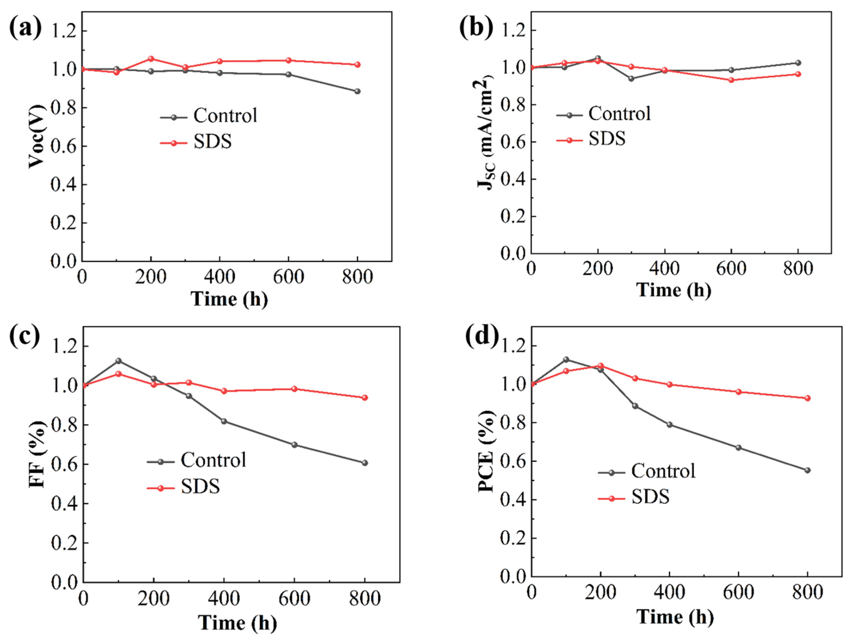
To test the stability of the device, we placed the prepared device in a glove box filled with N
2 for the stability test of the device, as shown in
Figure 7. We tested the performance of the device for
800 h. According to the test results in
Figure 7, it can be known that the performance of the control group device only maintained about
60% of the original after
800 h of stability test. However, the devices modified by SDS maintained about
90% of the original. The improvement in the stability of the devices is attributed to the perovskite films with higher quality and fewer defect states.
3. Experimental
3.1. Materials
Lead (II) nitrate (Pb(NO3)2, 99.99%) and isopropanol (IPA, 99.8%) were purchased from Aladdin (Shanghai, China). PEDOT:PSS (Heraeus Clevios AI 4083, 1.3–1.7% in H2O dispersion), methylammonium iodide (MAI, 99.5%), methylammonium chloride (MACl, 99.5%), -phenyl C61-butyric acid methyl ester (PC61BM, 99.5%), and bathocuproine (BCP, 99.0%) were obtained from Xi’an Yuri Solar Co., Ltd. (Xi’an, China). Chlorobenzene (CB, 99.8%, ultra-dry) was sourced from MERYER (Shanghai, China). Indium tin oxide (ITO) substrates with a sheet resistance of ~15 Ω/□ were procured from Advanced Election Technology Co., Ltd. (Shenzhen, China).
3.2. Device Fabrication
The ITO glass substrates were sequentially cleaned through the following procedure: first, ultrasonic cleaning with detergent at 55 °C for 1 h using a KQ3200DV cleaner (Shumei, Kunshan, China), followed by at least three cycles of ultrasonic rinsing with deionized water (10 min per cycle), and finally dried under a dry N2 stream. A PEDOT:PSS solution (VPEDOT:PSS:Vwater = 1:6) was spin-coated onto the ITO substrates at 6000 rpm for 40 s after 1 min of static deposition, followed by thermal annealing at 150 °C for 30 min. The substrates were then transferred into a custom-built glove box maintained at 20% relative humidity (RH).
Perovskite films were fabricated using a sequential deposition method. First, an aqueous Pb(NO3)2 solution (1.8 M) was spin-coated onto the PEDOT:PSS layer at 4000 rpm for 30 s, followed by immediate annealing at 100 °C for 10 min. Subsequently, the Pb(NO3)2 films were subjected to two cycles of MAX solution immersion (15 mg·mL−1 in IPA, WMAI:WMACl = 4:1) to form the control perovskite films. Notably, the films were rinsed with IPA after each immersion to remove by-products. For SDS-treated devices, SDS solutions of varying concentrations (1, 0.1, and 0.001 mg·mL−1 in deionized water) were used as the solvent while maintaining the Pb(NO3)2 concentration at 1.8 M. All other processing steps remained identical to those of the control films. Following the immersion process, the films were annealed at 100 °C for 30 min. The device fabrication continued with spin-coating of PC61BM (20 mg·mL−1 in CB) at 3000 rpm for 30 s, followed by annealing at 90 °C for 30 min. A BCP layer (0.5 mg·mL−1 in IPA) was then deposited by spin-coating at 2000 rpm for 30 s. Finally, Ag cathodes (~120 nm) were thermally evaporated under a vacuum of 1 × 10⁻⁴ Pa, completing the planar inverted PSCs with the structure of ITO/PEDOT:PSS /Perovskite/PC61BM/BCP/Ag. The fabricated devices had an effective area of 0.0625 cm2.
3.3. Characterizations
The J-V curves and steady-state output of the devices were gained by a source meter (Keithley, 2400, Cleveland, OH, USA) under the simulated light (AM 1.5G, 100 mW·cm−2) from a Newport simulator (94043A; Irvine, CA, USA). The EQE was tested by calculating the photocurrent and light intensity, measured using a lock-in amplifier (SR-830; Stanford Research Systems, Sunnyvale, CA, USA) by focusing a monochromatic light beam onto devices and a calibrated silicon detector, respectively. The phase and crystallinity of the films were tested by X-ray diffraction (XRD, Shimadzu, 7000, Kyoto, Japan) with a Cu Kα radiation source under 40 kV and 30 mA. Electrochemical impedance spectra (EIS) were measured with the electrochemical workstation (Chenhua, 660D, Shanghai, China) on a probe station (TTPX, Lakeshore, Westerville, OH, USA). The morphology of the perovskite film was characterized by scanning electron microscopy (SEM, JSM-6700F, JEOL Ltd., Akishima, Tokyo, Japan) at an accelerating voltage of 10 kV. For the test of transient photovoltage (TPV) and transient photocurrent (TPC), a pulsed laser with a pulse width of 6 ns and a wavelength of 532 nm was used as the excitation light source, and the Agilent DSO-X 3102A oscilloscope (Santa Clara, CA, USA) with a bandwidth of 1 GHz was adopted to collect the decays of voltage and current. UV-Vis absorption spectra in the range of 300–900 nm were obtained with the commercial spectrophotometer (Shimadzu UV-2550). The energy levels were measured by ultraviolet photoelectron spectroscopy (UPS, Shimadzu, AXIS SUPRA+, Japan). Surface roughness was quantified using atomic force microscopy (AFM) with the CSPM 5500 system. Contact angles (CA) were diligently measured using a contact angle goniometer (YIKE-360A, Chengde Precision Test Instrument Factory, Chengde, China). The FTIR spectra were recorded with a Spectrum Two 20A10370 of PE (PerkinElmer, Waltham, MA, USA). An FLS1000 instrument from Edinburgh Instruments (Livingston Village, UK) achieved steady-state photoluminescence (PL).


