
Advancing Graphene Synthesis: Low-Temperature Growth and Hydrogenation Mechanisms Using Plasma-Enhanced Chemical Vapor Deposition

 , ,
, ,  , and
, and
Abstract

1. Introduction
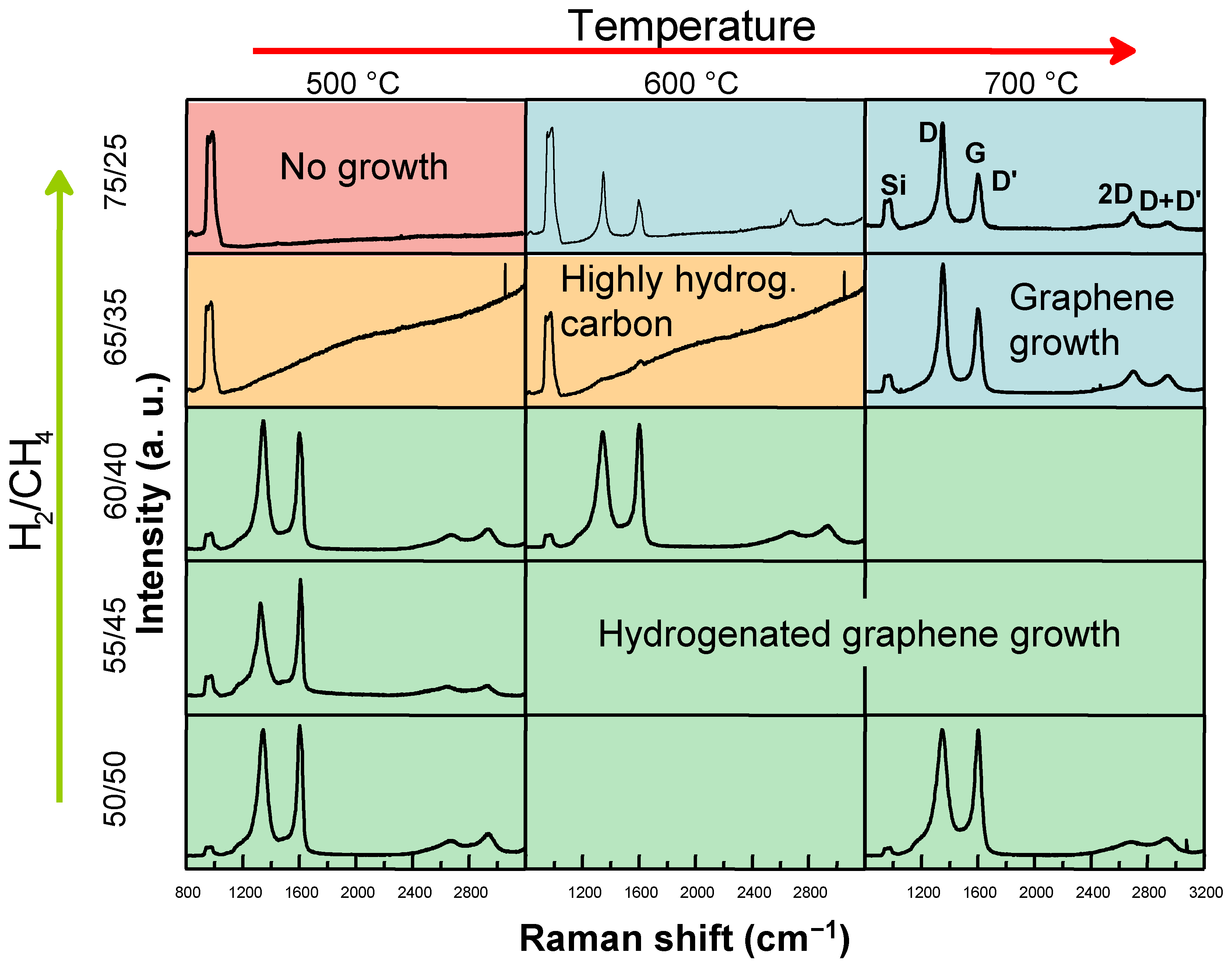
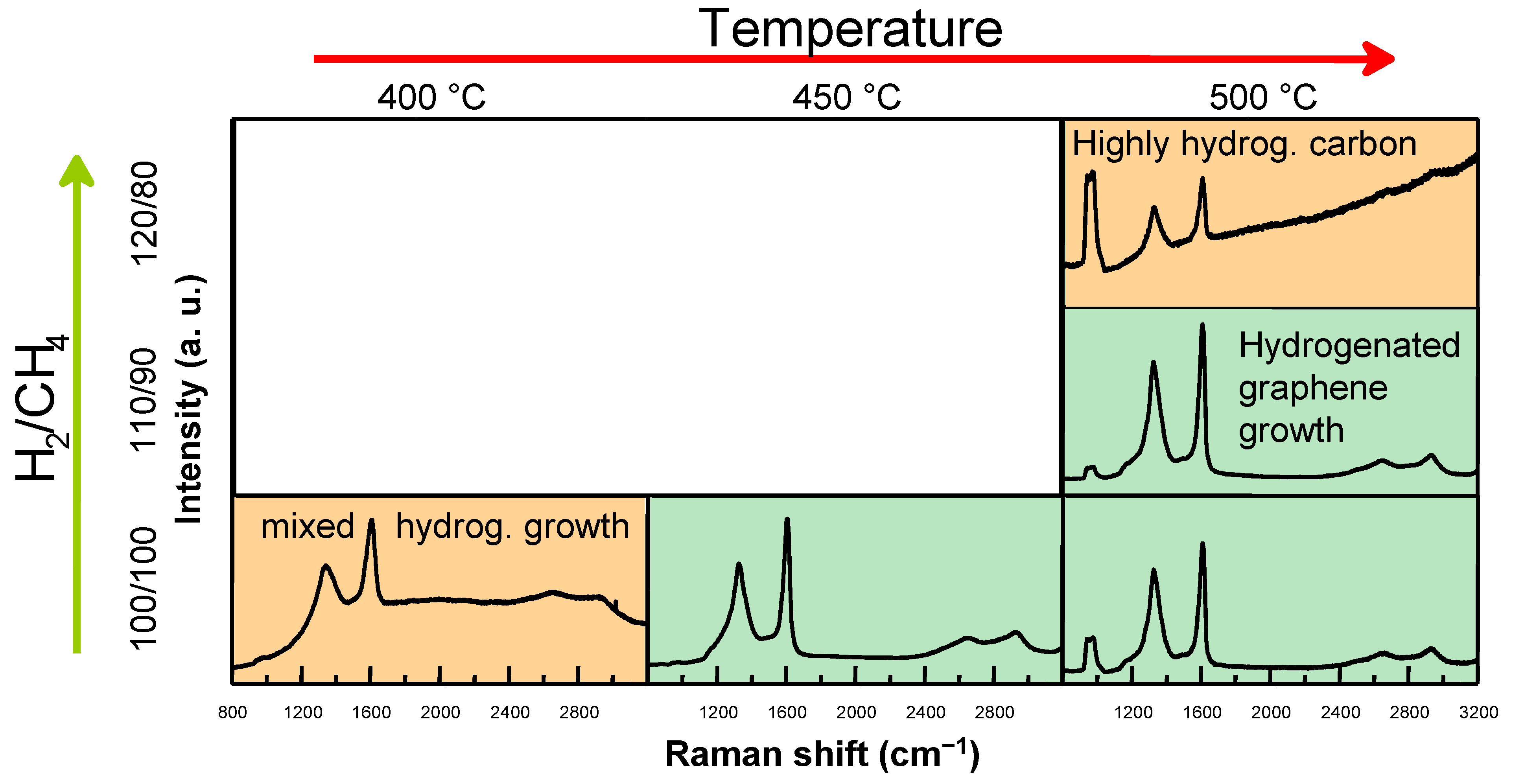
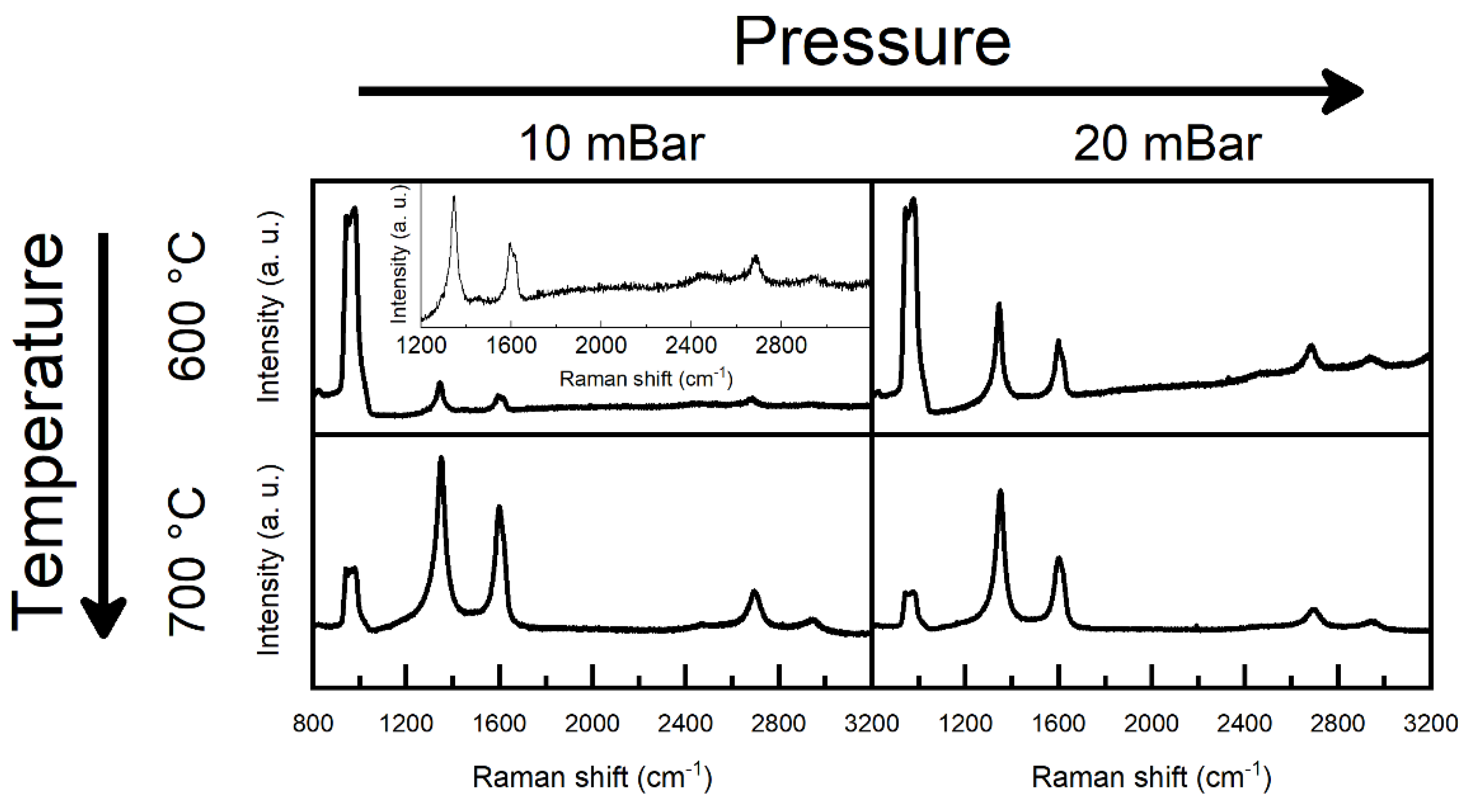
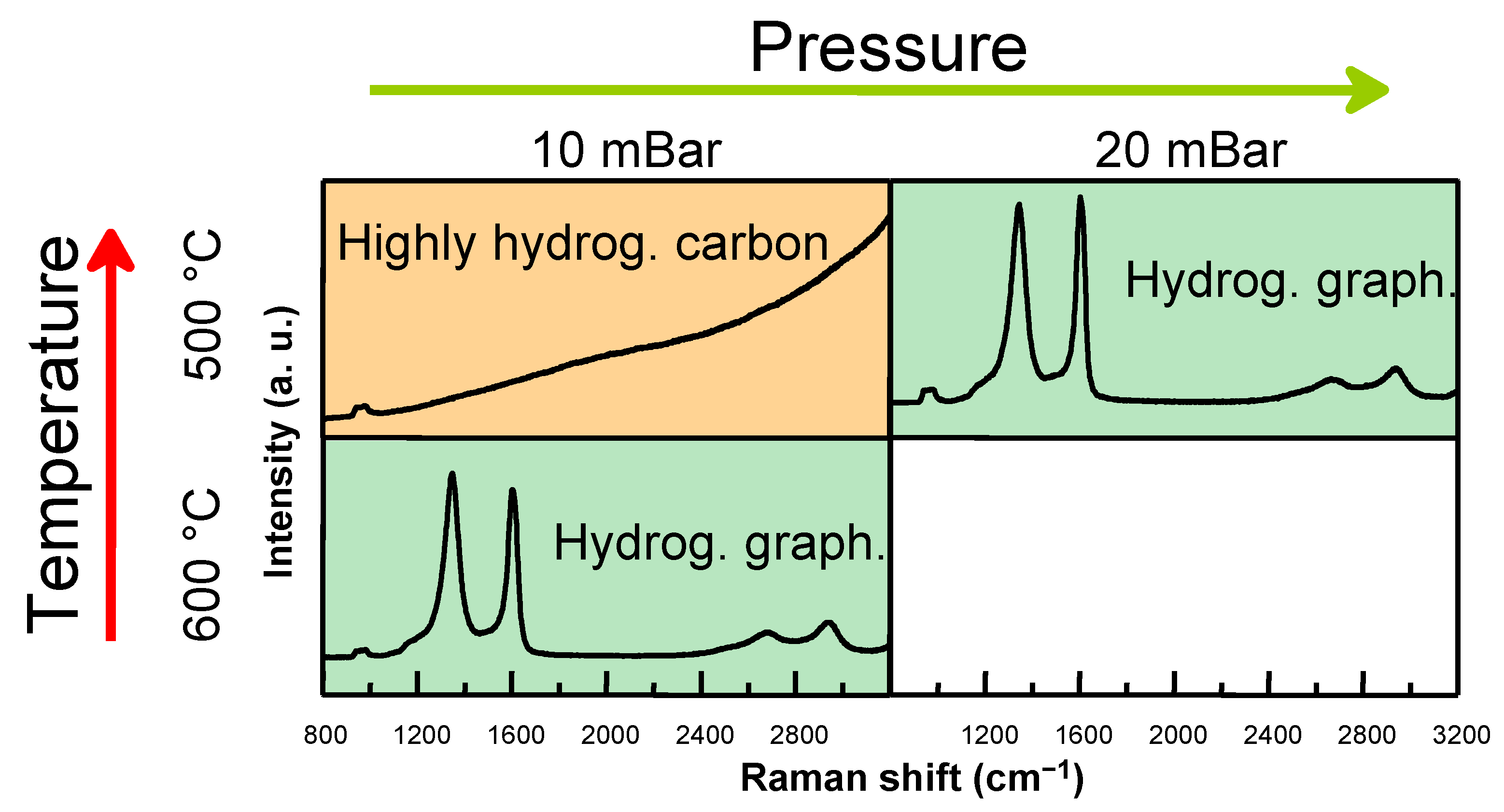
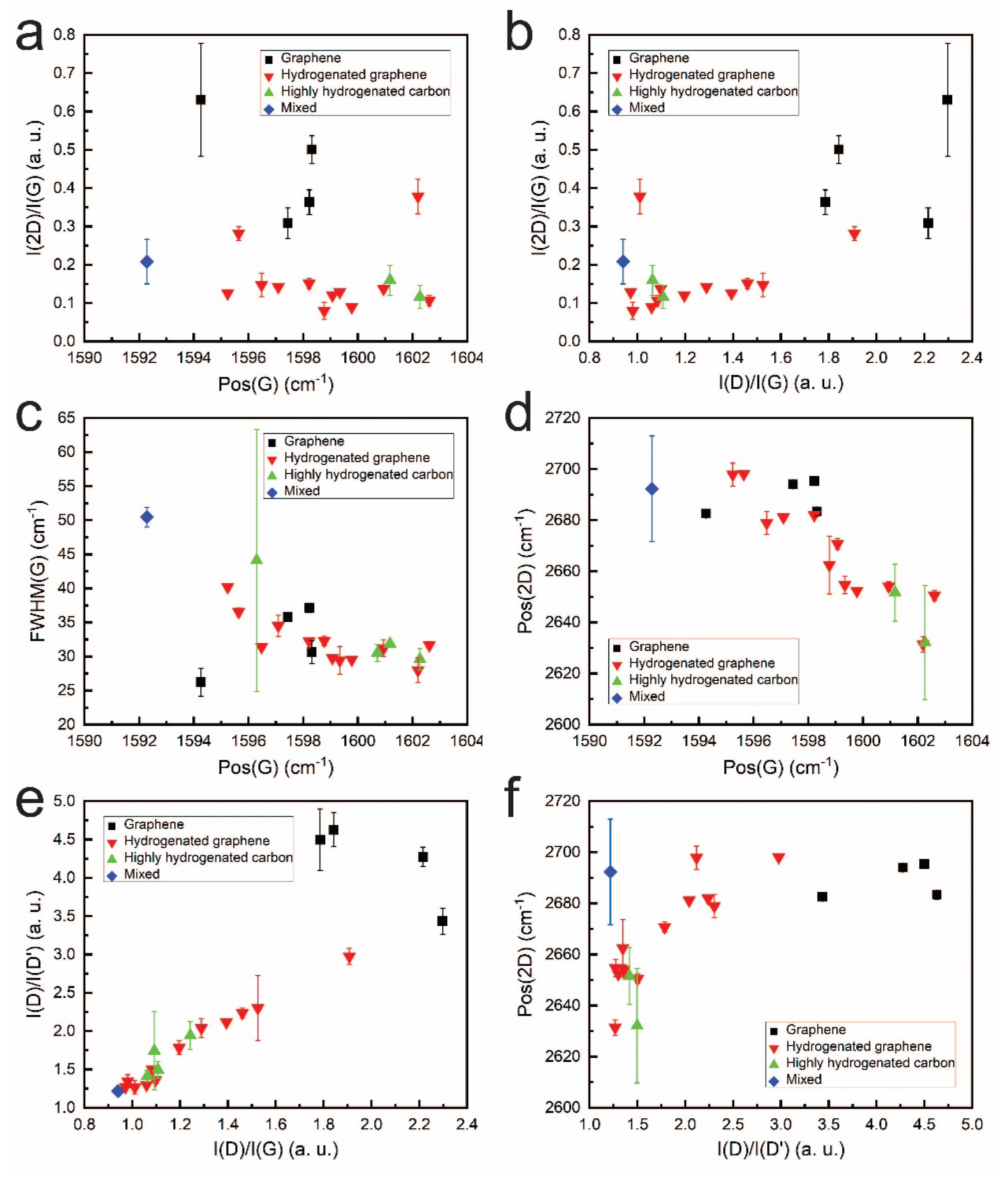
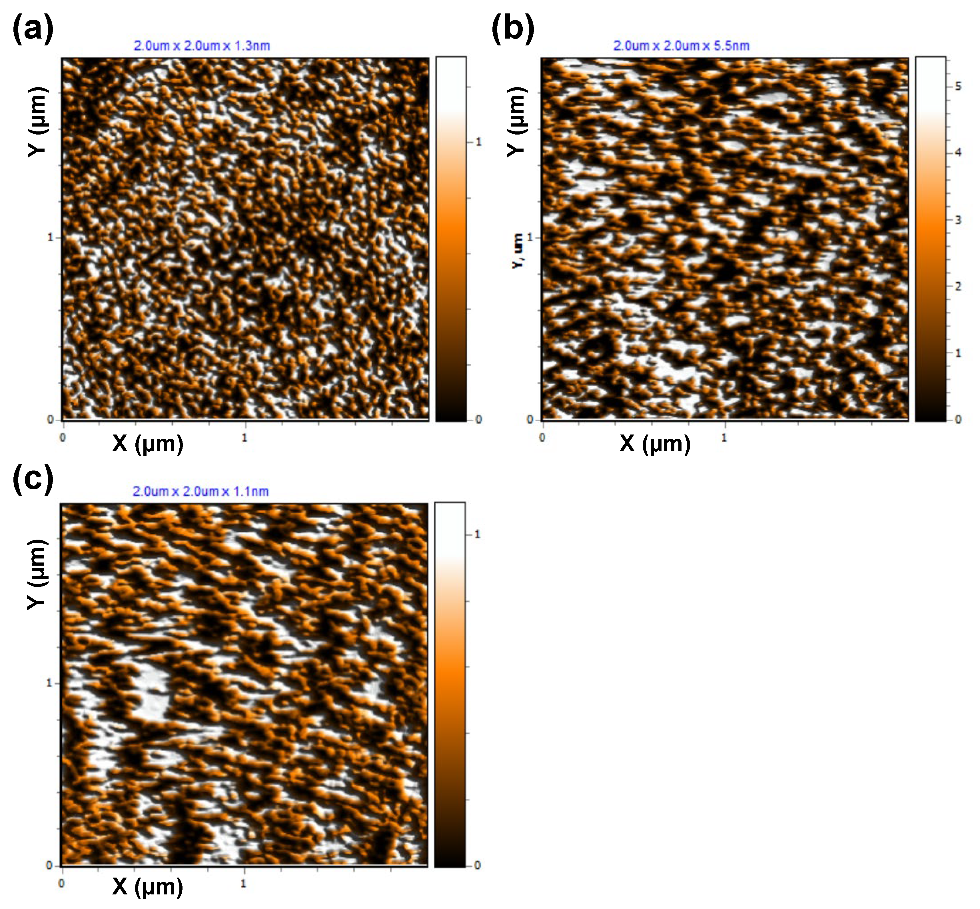
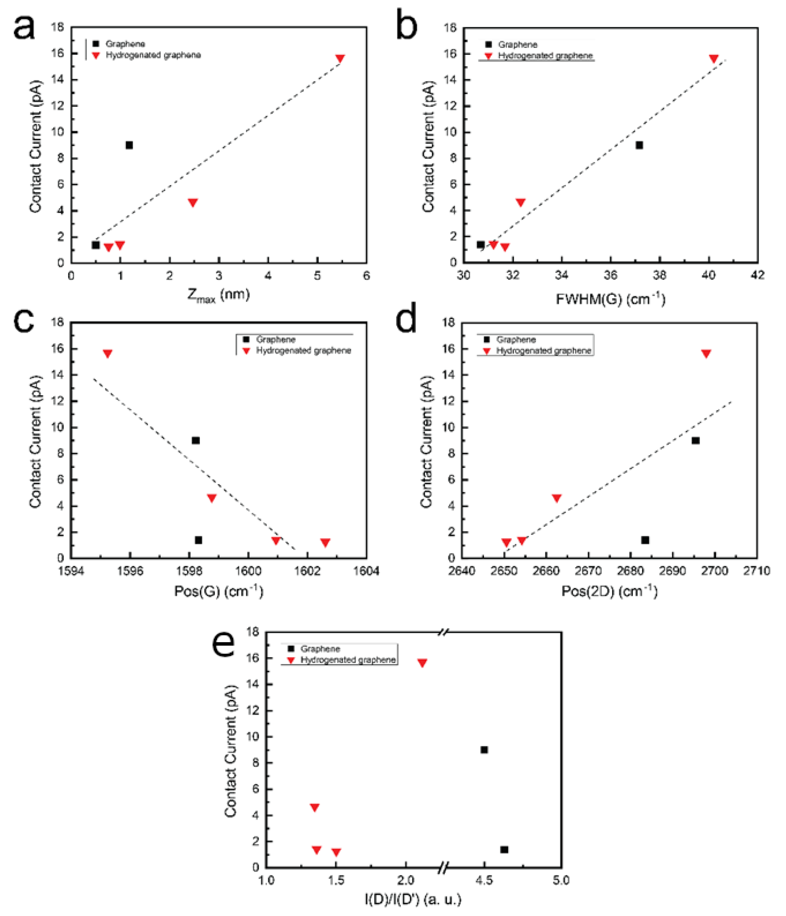
2. Results
3. Materials and Methods
4. Conclusions
Supplementary Materials
Author Contributions
Funding
Institutional Review Board Statement
Informed Consent Statement
Data Availability Statement
Conflicts of Interest
References
- Liao, L.; Lin, Y.-C.; Bao, M.; Cheng, R.; Bai, J.; Liu, Y.; Qu, Y.; Wang, K.L.; Huang, Y.; Duan, X. High-speed graphene transistors with a self-aligned nanowire gate. Nature 2010, 467, 305–308. [Google Scholar] [CrossRef] [PubMed]
- Miao, X.; Tongay, S.; Petterson, M.K.; Berke, K.; Rinzler, A.G.; Appleton, B.R.; Hebard, A.F. High efficiency graphene solar cells by chemical doping. Nano Lett. 2012, 12, 2745–2750. [Google Scholar] [CrossRef] [PubMed]
- Lee, C.; Wei, X.; Kysar, J.W.; Hone, J. Measurement of the elastic properties and intrinsic strength of monolayer graphene. Science 2008, 321, 385–388. [Google Scholar] [CrossRef] [PubMed]
- Tielrooij, K.-J.; Song, J.; Jensen, S.A.; Centeno, A.; Pesquera, A.; Zurutuza Elorza, A.; Bonn, M.; Levitov, L.; Koppens, F. Photoexcitation cascade and multiple hot-carrier generation in graphene. Nat. Phys. 2013, 9, 248–252. [Google Scholar] [CrossRef]
- Tung, T.T.; Nine, M.J.; Krebsz, M.; Pasinszki, T.; Coghlan, C.J.; Tran, D.N.; Losic, D. Recent advances in sensing applications of graphene assemblies and their composites. Adv. Funct. Mater. 2017, 27, 1702891. [Google Scholar] [CrossRef]
- Olabi, A.G.; Abdelkareem, M.A.; Wilberforce, T.; Sayed, E.T. Application of graphene in energy storage device—A review. Renew. Sustain. Energy Rev. 2021, 135, 110026. [Google Scholar] [CrossRef]
- Kauling, A.P.; Seefeldt, A.T.; Pisoni, D.P.; Pradeep, R.C.; Bentini, R.; Oliveira, R.V.; Novoselov, K.S.; Castro Neto, A.H. The worldwide graphene flake production. Adv. Mater. 2018, 30, 1803784. [Google Scholar] [CrossRef]
- Zheng, W.; Zhao, X.; Fu, W. Review of vertical graphene and its applications. ACS Appl. Mater. Interfaces 2021, 13, 9561–9579. [Google Scholar] [CrossRef]
- Pumera, M.; Wong, C.H.A. Graphane and hydrogenated graphene. Chem. Soc. Rev. 2013, 42, 5987–5995. [Google Scholar] [CrossRef]
- Deng, B.; Liu, Z.; Peng, H. Toward mass production of CVD graphene films. Adv. Mater. 2019, 31, 1800996. [Google Scholar] [CrossRef]
- Yi, M.; Shen, Z. A review on mechanical exfoliation for the scalable production of graphene. J. Mater. Chem. A 2015, 3, 11700–11715. [Google Scholar] [CrossRef]
- Kuila, T.; Bose, S.; Khanra, P.; Mishra, A.K.; Kim, N.H.; Lee, J.H. Recent advances in graphene-based biosensors. Biosens. Bioelectron. 2011, 26, 4637–4648. [Google Scholar] [CrossRef] [PubMed]
- Xu, Y.; Cheng, C.; Du, S.; Yang, J.; Yu, B.; Luo, J.; Yin, W.; Li, E.; Dong, S.; Ye, P. Contacts between two-and three-dimensional materials: Ohmic, Schottky, and p–n heterojunctions. ACS Nano 2016, 10, 4895–4919. [Google Scholar] [CrossRef] [PubMed]
- Di Bartolomeo, A. Graphene Schottky diodes: An experimental review of the rectifying graphene/semiconductor heterojunction. Phys. Rep. 2016, 606, 1–58. [Google Scholar] [CrossRef]
- Wei, D.; Lu, Y.; Han, C.; Niu, T.; Chen, W.; Wee, A.T.S. Critical crystal growth of graphene on dielectric substrates at low temperature for electronic devices. Angew. Chem. 2013, 52, 14121–14126. [Google Scholar] [CrossRef]
- Li, M.; Liu, D.; Wei, D.; Song, X.; Wei, D.; Wee, A.T.S. Controllable synthesis of graphene by plasma-enhanced chemical vapor deposition and its related applications. Adv. Sci. 2016, 3, 1600003. [Google Scholar] [CrossRef]
- Gudaitis, R.; Lazauskas, A.; Jankauskas, Š.; Meškinis, Š. Catalyst-less and transfer-less synthesis of graphene on Si (100) using direct microwave plasma enhanced chemical vapor deposition and protective enclosures. Materials 2020, 13, 5630. [Google Scholar] [CrossRef]
- Qi, Y.; Deng, B.; Guo, X.; Chen, S.; Gao, J.; Li, T.; Dou, Z.; Ci, H.; Sun, J.; Chen, Z. Switching vertical to horizontal graphene growth using faraday cage-assisted PECVD approach for high-performance transparent heating device. Adv. Mater. 2018, 30, 1704839. [Google Scholar] [CrossRef]
- Meškinis, Š.; Vasiliauskas, A.; Guobienė, A.; Talaikis, M.; Niaura, G.; Gudaitis, R. The direct growth of planar and vertical graphene on Si (100) via microwave plasma chemical vapor deposition: Synthesis conditions effects. RSC Adv. 2022, 12, 18759–18772. [Google Scholar] [CrossRef]
- Meškinis, Š.; Gudaitis, R.; Vasiliauskas, A.; Tamulevičius, S.; Niaura, G. Multiwavelength Raman Scattering Spectroscopy Study of Graphene Synthesized on Si (100) and SiO2 by Microwave Plasma-Enhanced Chemical Vapor Deposition. Phys. Status Solidi (RRL) Rapid Res. Lett. 2020, 14, 1900462. [Google Scholar] [CrossRef]
- Ferrari, A.C.; Basko, D.M. Raman spectroscopy as a versatile tool for studying the properties of graphene. Nat. Nanotechnol. 2013, 8, 235–246. [Google Scholar] [CrossRef] [PubMed]
- Merlen, A.; Buijnsters, J.G.; Pardanaud, C. A guide to and review of the use of multiwavelength Raman spectroscopy for characterizing defective aromatic carbon solids: From graphene to amorphous carbons. Coatings 2017, 7, 153. [Google Scholar] [CrossRef]
- Piazza, F.; Gough, K.; Monthioux, M.; Puech, P.; Gerber, I.; Wiens, R.; Paredes, G.; Ozoria, C. Low temperature, pressureless sp2 to sp3 transformation of ultrathin, crystalline carbon films. Carbon 2019, 145, 10–22. [Google Scholar] [CrossRef]
- Luo, Z.; Yu, T.; Kim, K.-j.; Ni, Z.; You, Y.; Lim, S.; Shen, Z.; Wang, S.; Lin, J. Thickness-dependent reversible hydrogenation of graphene layers. ACS Nano 2009, 3, 1781–1788. [Google Scholar] [CrossRef]
- Elias, D.C.; Nair, R.R.; Mohiuddin, T.; Morozov, S.; Blake, P.; Halsall, M.; Ferrari, A.C.; Boukhvalov, D.; Katsnelson, M.; Geim, A. Control of graphene’s properties by reversible hydrogenation: Evidence for graphane. Science 2009, 323, 610–613. [Google Scholar] [CrossRef]
- Melios, C.; Spencer, S.; Shard, A.; Strupiński, W.; Silva, S.R.P.; Kazakova, O. Surface and interface structure of quasi-free standing graphene on SiC. 2D Mater. 2016, 3, 025023. [Google Scholar] [CrossRef]
- Shtepliuk, I.; Ivanov, I.G.; Iakimov, T.; Yakimova, R.; Kakanakova-Georgieva, A.; Fiorenza, P.; Giannazzo, F. Raman probing of hydrogen-intercalated graphene on Si-face 4H-SiC. Mater. Sci. Semicond. Process. 2019, 96, 145–152. [Google Scholar] [CrossRef]
- Meškinis, Š.; Vasiliauskas, A.; Gudaitis, R.; Andrulevičius, M.; Guobienė, A. Direct graphene synthesis on Si (1 0 0) by inductively coupled plasma beam source. Appl. Surf. Sci. 2022, 580, 152265. [Google Scholar] [CrossRef]
- Casiraghi, C.; Piazza, F.; Ferrari, A.; Grambole, D.; Robertson, J. Bonding in hydrogenated diamond-like carbon by Raman spectroscopy. Diam. Relat. Mater. 2005, 14, 1098–1102. [Google Scholar] [CrossRef]
- Cloutis, E.; Szymanski, P.; Applin, D.; Goltz, D. Identification and discrimination of polycyclic aromatic hydrocarbons using Raman spectroscopy. Icarus 2016, 274, 211–230. [Google Scholar] [CrossRef]
- Hwang, J.-S.; Lin, Y.-H.; Hwang, J.-Y.; Chang, R.; Chattopadhyay, S.; Chen, C.-J.; Chen, P.; Chiang, H.-P.; Tsai, T.-R.; Chen, L.-C. Imaging layer number and stacking order through formulating Raman fingerprints obtained from hexagonal single crystals of few layer graphene. Nanotechnology 2012, 24, 015702. [Google Scholar] [CrossRef] [PubMed]
- Casiraghi, C. Probing disorder and charged impurities in graphene by Raman spectroscopy. Phys. Status Solidi (RRL) Rapid Res. Lett. 2009, 3, 175–177. [Google Scholar] [CrossRef]
- Casiraghi, C.; Pisana, S.; Novoselov, K.; Geim, A.K.; Ferrari, A. Raman fingerprint of charged impurities in graphene. Appl. Phys. Lett. 2007, 91, 233108. [Google Scholar] [CrossRef]
- Clapa, M.; Gaj, J. Behavior of graphene under glow discharge plasma. Sens. Actuators A Phys. 2021, 332, 113069. [Google Scholar] [CrossRef]
- Childres, I.; Jauregui, L.A.; Tian, J.; Chen, Y.P. Effect of oxygen plasma etching on graphene studied using Raman spectroscopy and electronic transport measurements. New J. Phys. 2011, 13, 025008. [Google Scholar] [CrossRef]
- Lee, J.E.; Ahn, G.; Shim, J.; Lee, Y.S.; Ryu, S. Optical separation of mechanical strain from charge doping in graphene. Nat. Commun. 2012, 3, 1024. [Google Scholar] [CrossRef]
- Fates, R.; Bouridah, H.; Raskin, J.-P. Probing carrier concentration in gated single, bi-and tri-layer CVD graphene using Raman spectroscopy. Carbon 2019, 149, 390–399. [Google Scholar] [CrossRef]
- Bong, J.H.; Sul, O.; Yoon, A.; Choi, S.-Y.; Cho, B.J. Facile graphene n-doping by wet chemical treatment for electronic applications. Nanoscale 2014, 6, 8503–8508. [Google Scholar] [CrossRef]
- Jankauskas, Š.; Gudaitis, R.; Vasiliauskas, A.; Guobienė, A.; Meškinis, Š. The graphene structure’s effects on the current-voltage and photovoltaic characteristics of directly synthesized graphene/n-Si (100) diodes. Nanomaterials 2022, 12, 1640. [Google Scholar] [CrossRef]
- Meškinis, Š.; Gudaitis, R.; Vasiliauskas, A.; Guobienė, A.; Jankauskas, Š.; Stankevič, V.; Keršulis, S.; Stirkė, A.; Andriukonis, E.; Melo, W. Biosensor based on graphene directly grown by MW-PECVD for detection of COVID-19 spike (S) protein and its entry receptor ACE2. Nanomaterials 2023, 13, 2373. [Google Scholar] [CrossRef]
- Shi, Y.; Dong, X.; Chen, P.; Wang, J.; Li, L.-J. Effective doping of single-layer graphene from underlying SiO2 substrates. Phys. Rev. B Condens. Matter Mater. Phys. 2009, 79, 115402. [Google Scholar] [CrossRef]
- Wittmann, S.; Aumer, F.; Wittmann, D.; Pindl, S.; Wagner, S.; Gahoi, A.; Reato, E.; Belete, M.; Kataria, S.; Lemme, M.C. Dielectric surface charge engineering for electrostatic doping of graphene. ACS Appl. Electron. Mater. 2020, 2, 1235–1242. [Google Scholar] [CrossRef]
- Kang, Y.-J.; Kang, J.; Chang, K.-J. Electronic structure of graphene and doping effect on SiO2. Phys. Rev. B Condens. Matter Mater. Phys. 2008, 78, 115404. [Google Scholar] [CrossRef]
- Banszerus, L.; Janssen, H.; Otto, M.; Epping, A.; Taniguchi, T.; Watanabe, K.; Beschoten, B.; Neumaier, D.; Stampfer, C. Identifying suitable substrates for high-quality graphene-based heterostructures. 2D Mater. 2017, 4, 025030. [Google Scholar] [CrossRef]
- Jee, H.-g.; Jin, K.-H.; Han, J.-H.; Hwang, H.-N.; Jhi, S.-H.; Kim, Y.D.; Hwang, C.-C. Controlling the self-doping of epitaxial graphene on SiC via Ar ion treatment. Phys. Rev. B Condens. Matter Mater. Phys. 2011, 84, 075457. [Google Scholar] [CrossRef]
- Eriksson, J.; Puglisi, D.; Vasiliauskas, R.; Lloyd Spetz, A.; Yakimova, R. Thickness uniformity and electron doping in epitaxial graphene on SiC. Mater. Sci. Forum 2013, 740–742, 153–156. [Google Scholar] [CrossRef]
- Goniszewski, S.; Adabi, M.; Shaforost, O.; Hanham, S.; Hao, L.; Klein, N. Correlation of p-doping in CVD Graphene with Substrate Surface Charges. Sci. Rep. 2016, 6, 22858. [Google Scholar] [CrossRef]
- Eckmann, A.; Felten, A.; Mishchenko, A.; Britnell, L.; Krupke, R.; Novoselov, K.S.; Casiraghi, C. Probing the nature of defects in graphene by Raman spectroscopy. Nano Lett. 2012, 12, 3925–3930. [Google Scholar] [CrossRef]
- Venezuela, P.; Lazzeri, M.; Mauri, F. Theory of double-resonant Raman spectra in graphene: Intensity and line shape of defect-induced and two-phonon bands. Phys. Rev. B Condens. Matter Mater. Phys. 2011, 84, 035433. [Google Scholar] [CrossRef]
- Whitener, K.E. Hydrogenated graphene: A user’s guide. J. Vac. Sci. Technol. A 2018, 36, 05G401. [Google Scholar] [CrossRef]
- Matis, B.R.; Burgess, J.S.; Bulat, F.A.; Friedman, A.L.; Houston, B.H.; Baldwin, J.W. Surface doping and band gap tunability in hydrogenated graphene. ACS Nano 2012, 6, 17–22. [Google Scholar] [CrossRef] [PubMed]
- Ma, Y.; Harding, J.D.; Tu, X. Catalyst-free low temperature conversion of n-dodecane for co-generation of COx-free hydrogen and C2 hydrocarbons using a gliding arc plasma. Int. J. Hydrog. Energy 2019, 44, 26158–26168. [Google Scholar] [CrossRef]
- Wang, S.; Wang, J.; Feng, D.; Wang, F.; Zhao, Y.; Sun, S. Plasma-induced methane catalytic cracking: Effects of experimental conditions. Int. J. Hydrog. Energy 2024, 63, 284–293. [Google Scholar] [CrossRef]
- Muñoz, R.; Munuera, C.; Martínez, J.I.; Azpeitia, J.; Gómez-Aleixandre, C.; García-Hernández, M. Low temperature metal free growth of graphene on insulating substrates by plasma assisted chemical vapor deposition. 2D Mater. 2016, 4, 015009. [Google Scholar] [CrossRef] [PubMed]
- Chaitoglou, S.; Bertran, E. Effect of temperature on graphene grown by chemical vapor deposition. J. Mater. Sci. 2017, 52, 8348–8356. [Google Scholar] [CrossRef]
- Klingsporn, M.; Kirner, S.; Villringer, C.; Abou-Ras, D.; Costina, I.; Lehmann, M.; Stannowski, B. Resolving the nanostructure of plasma-enhanced chemical vapor deposited nanocrystalline SiOx layers for application in solar cells. J. Appl. Phys. 2016, 119, 223104. [Google Scholar] [CrossRef]
- Bo, Z.; Yang, Y.; Chen, J.; Yu, K.; Yan, J.; Cen, K. Plasma-enhanced chemical vapor deposition synthesis of vertically oriented graphene nanosheets. Nanoscale 2013, 5, 5180–5204. [Google Scholar] [CrossRef]
- Dresselhaus, M.; Jorio, A.; Souza Filho, A.; Saito, R. Defect characterization in graphene and carbon nanotubes using Raman spectroscopy. Philos. Trans. R. Soc. A Math. Phys. Eng. Sci. 2010, 368, 5355–5377. [Google Scholar] [CrossRef]
- No, Y.-S.; Choi, H.K.; Kim, J.-S.; Kim, H.; Yu, Y.-J.; Choi, C.-G.; Choi, J.S. Layer number identification of CVD-grown multilayer graphene using Si peak analysis. Sci. Rep. 2018, 8, 571. [Google Scholar] [CrossRef]

| Sample No | Temperature (°C) | H2 Flow (sccm) | CH4 Flow (sccm) | Pressure (mBar) |
|---|---|---|---|---|
| 1 | 700 | 75 | 25 | 20 |
| 2 | 700 | 75 | 25 | 10 |
| 3 | 600 | 75 | 25 | 20 |
| 4 | 600 | 75 | 25 | 10 |
| 5 | 500 | 75 | 25 | 20 |
| 6 | 700 | 65 | 35 | 20 |
| 7 | 600 | 65 | 35 | 20 |
| 8 | 500 | 65 | 35 | 20 |
| 9 | 600 | 60 | 40 | 20 |
| 10 | 500 | 60 | 40 | 20 |
| 11 | 500 | 55 | 45 | 20 |
| 12 | 700 | 50 | 50 | 20 |
| 13 | 600 | 50 | 50 | 10 |
| 14 | 500 | 50 | 50 | 20 |
| 15 | 500 | 50 | 50 | 10 |
| 16 | 500 | 120 | 80 | 20 |
| 17 | 500 | 110 | 90 | 20 |
| 18 | 500 | 100 | 100 | 20 |
| 19 | 450 | 100 | 100 | 20 |
| 20 | 400 | 100 | 100 | 20 |
| 21 | 500 | 100 | 100 | 10 |
| 22 | 500 | 75 | 75 | 20 |
| 23 | 500 | 80 | 70 | 20 |
Disclaimer/Publisher’s Note: The statements, opinions and data contained in all publications are solely those of the individual author(s) and contributor(s) and not of MDPI and/or the editor(s). MDPI and/or the editor(s) disclaim responsibility for any injury to people or property resulting from any ideas, methods, instructions or products referred to in the content. |
© 2024 by the authors. Licensee MDPI, Basel, Switzerland. This article is an open access article distributed under the terms and conditions of the Creative Commons Attribution (CC BY) license (https://creativecommons.org/licenses/by/4.0/).
Share and Cite
Meškinis, Š.; Lazauskas, A.; Jankauskas, Š.; Guobienė, A.; Gudaitis, R. Advancing Graphene Synthesis: Low-Temperature Growth and Hydrogenation Mechanisms Using Plasma-Enhanced Chemical Vapor Deposition. Molecules 2025, 30, 33. https://doi.org/10.3390/molecules30010033
Meškinis Š, Lazauskas A, Jankauskas Š, Guobienė A, Gudaitis R. Advancing Graphene Synthesis: Low-Temperature Growth and Hydrogenation Mechanisms Using Plasma-Enhanced Chemical Vapor Deposition. Molecules. 2025; 30(1):33. https://doi.org/10.3390/molecules30010033
Chicago/Turabian StyleMeškinis, Šarūnas, Algirdas Lazauskas, Šarūnas Jankauskas, Asta Guobienė, and Rimantas Gudaitis. 2025. "Advancing Graphene Synthesis: Low-Temperature Growth and Hydrogenation Mechanisms Using Plasma-Enhanced Chemical Vapor Deposition" Molecules 30, no. 1: 33. https://doi.org/10.3390/molecules30010033
APA StyleMeškinis, Š., Lazauskas, A., Jankauskas, Š., Guobienė, A., & Gudaitis, R. (2025). Advancing Graphene Synthesis: Low-Temperature Growth and Hydrogenation Mechanisms Using Plasma-Enhanced Chemical Vapor Deposition. Molecules, 30(1), 33. https://doi.org/10.3390/molecules30010033