
A Review of the Fabrication of Pinhole-Free Thin Films Based on Electrodeposition Technology: Theory, Methods and Progress


Abstract
1. Introduction
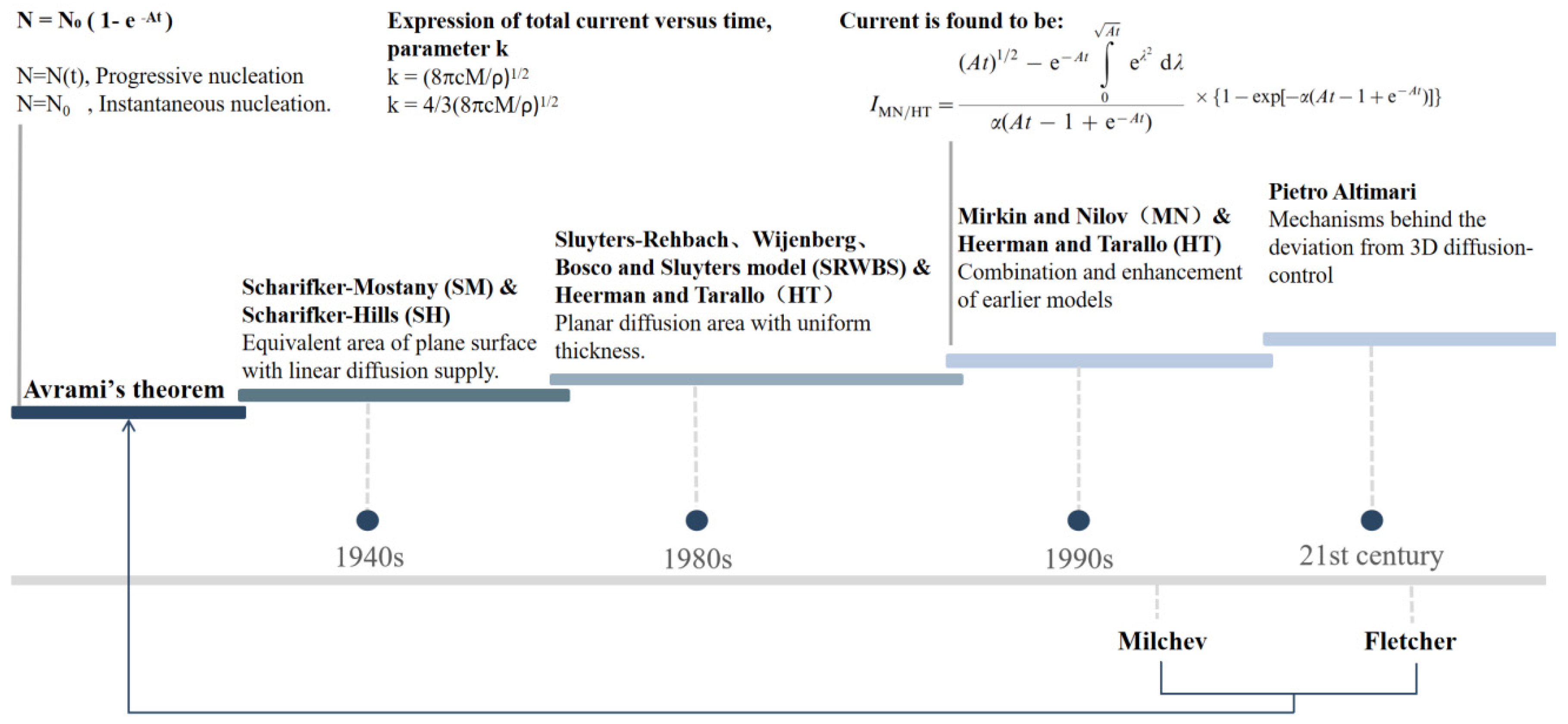
2. Theoretical Models and Mathematical Analysis of Particle Dynamics in Electrodeposition Technology
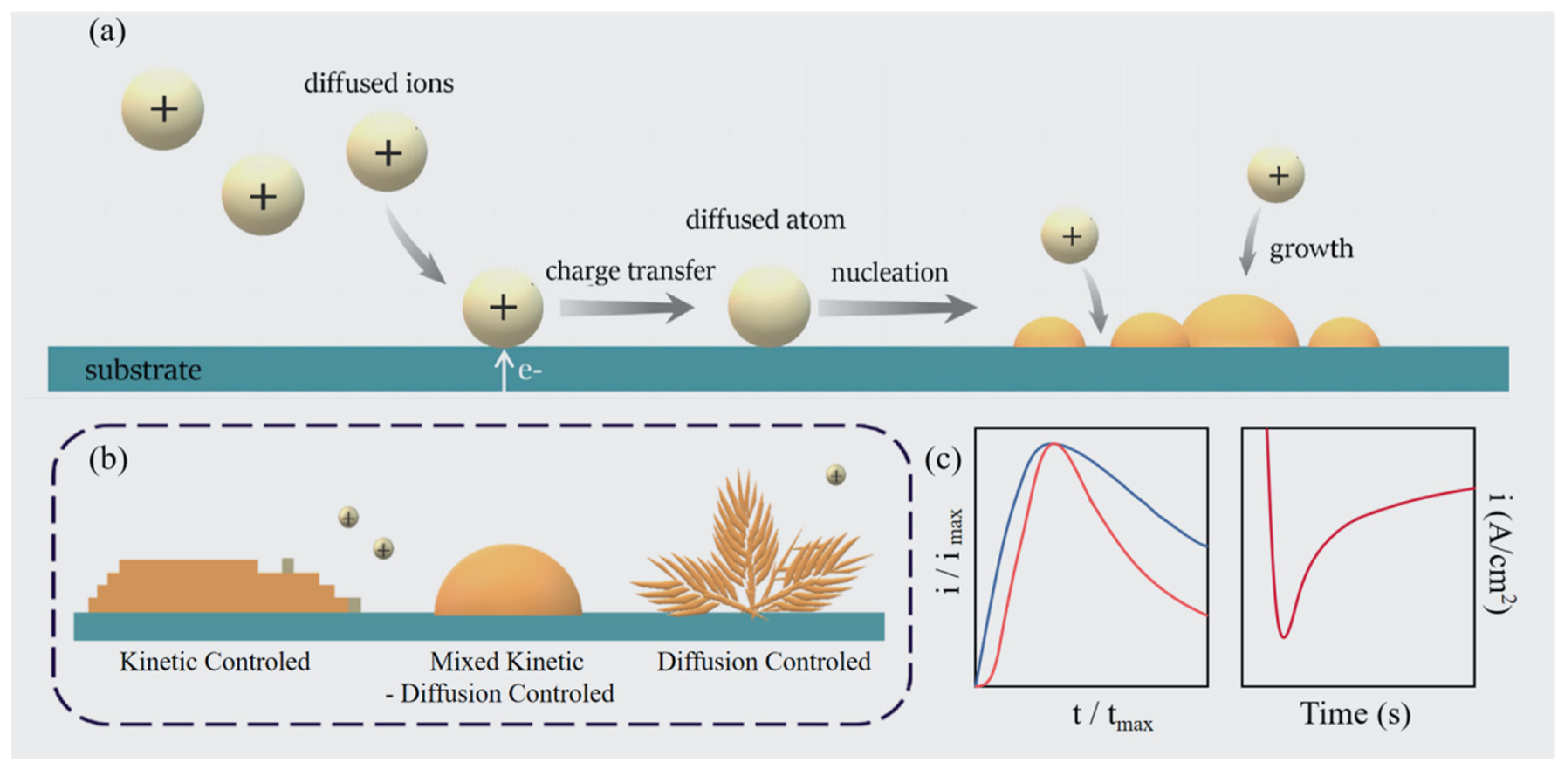
2.1. General Description of Electrodeposition Nucleation and Growth Theory
2.2. Growth Models Under Diffusion Control
2.3. Growth Models Under Mixed Kinetic–Diffusion Control
2.4. Growth Models Deviated from 3D Diffusion Zone Control
2.5. Particle Dynamics Theory Models and Their Specific Applications in Electrodeposition
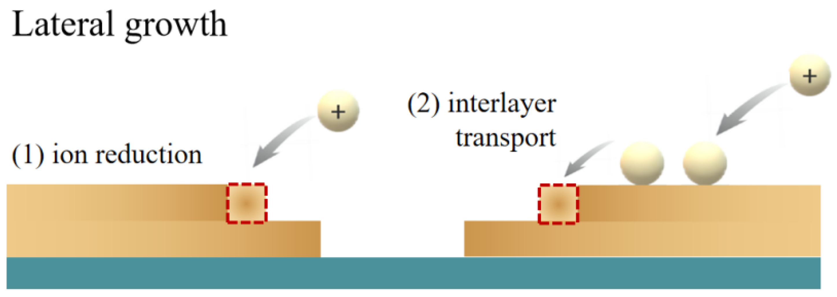
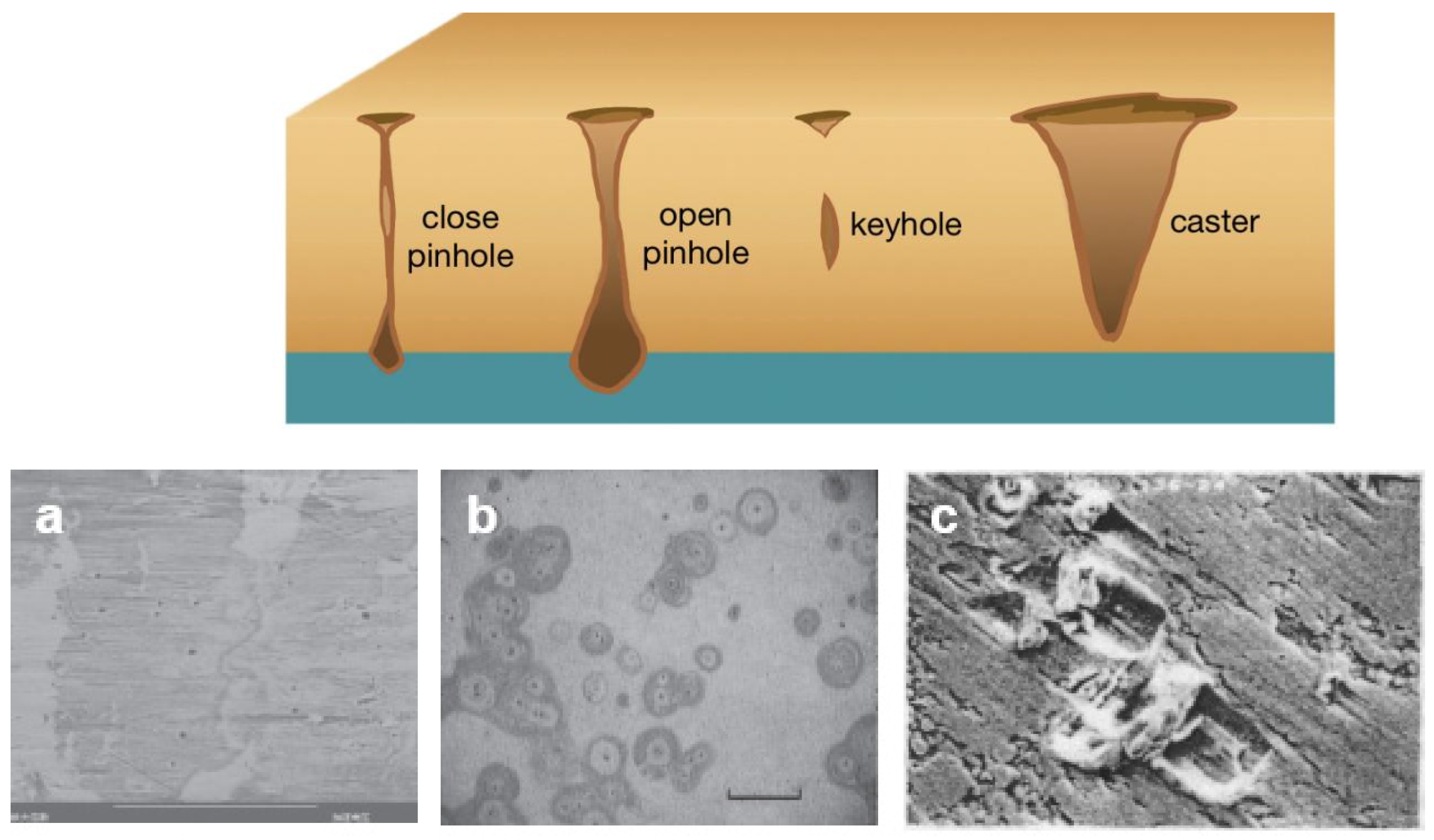
3. Formation Causes of Pinholes and Routes of Pinhole-Free Film Preparation
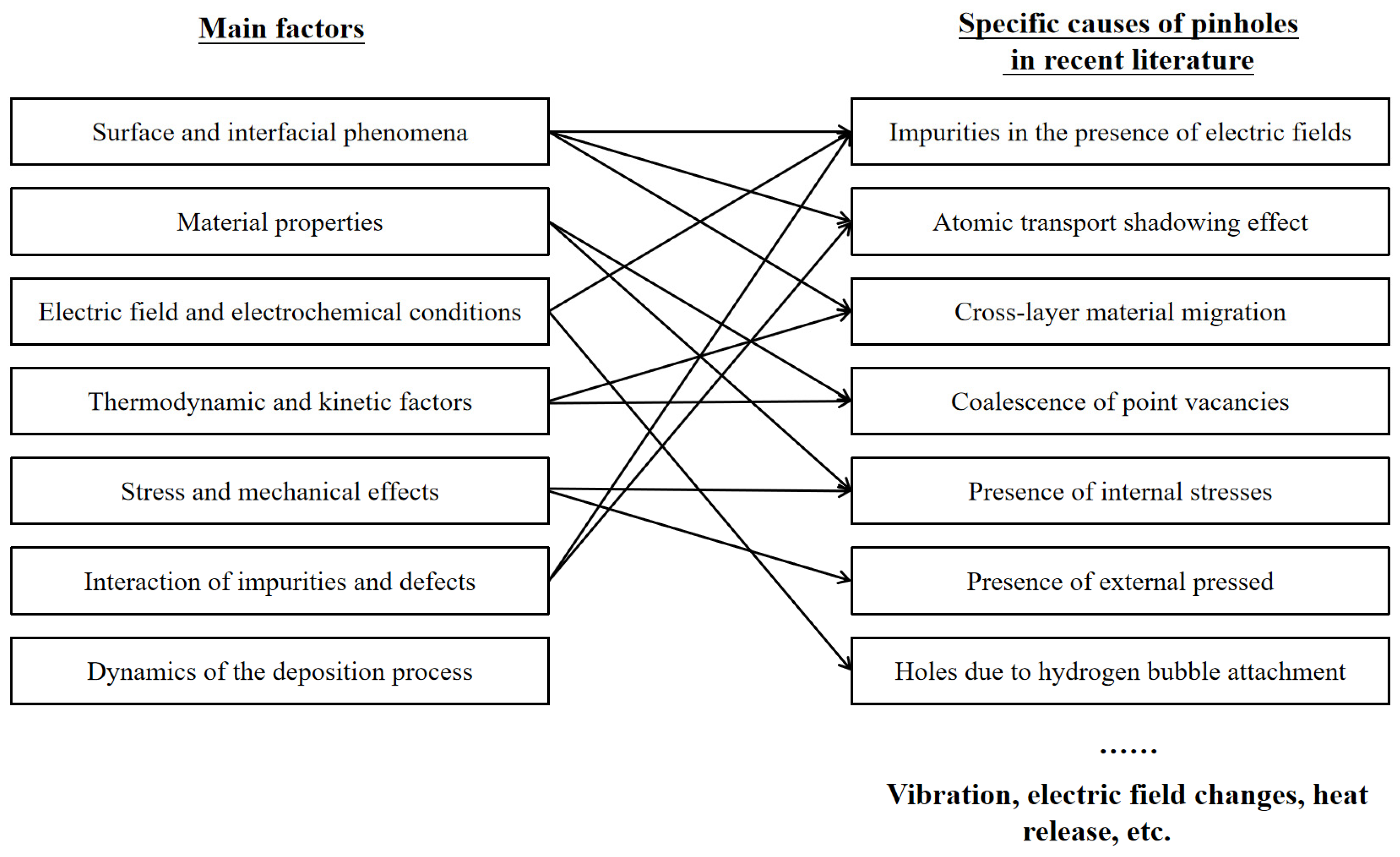
3.1. Formation Causes of Pinhole Defects
- (i)
- Impurities in the presence of electric fields
- (ii)
- Atomic transport shadowing effect
- (iii)
- Cross-layer material migration
- (iv)
- Coalescence of point vacancies
- (v)
- Presence of internal stresses
- (vi)
- Presence of external pressed
- (vii)
- Pits or holes formed by attached hydrogen bubbles
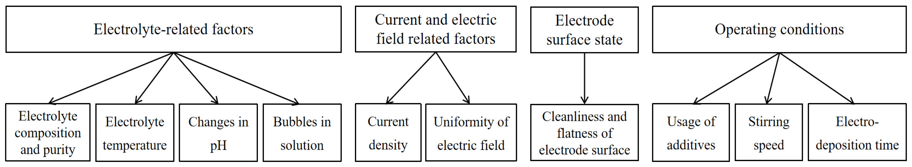
3.2. Discussion on Parameter Adjustment in the Electrodeposition Process
3.2.1. The Role of Anions in Influencing Nucleation, Growth and Particle Shape in Electrodeposition
3.2.2. Impact of Point Defects and Surface Diffusion in Electrodeposition
3.2.3. Strategies for Pinhole Mitigation in Thin Films
- I.
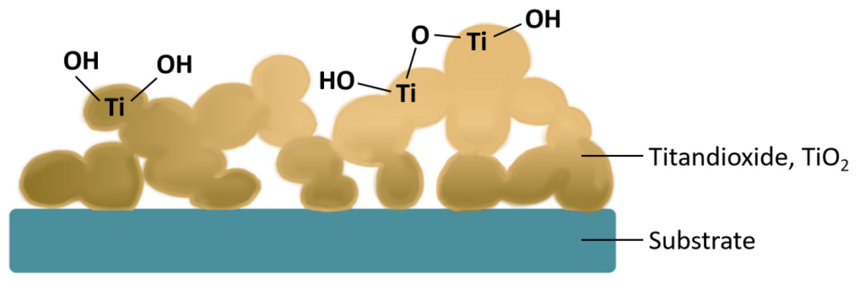
- Self-passivation of thin films. Hyun S. Ahn and Allen J. Bard [102] proposed an interesting way of constructing pinhole-free films through self-passivation using TiO2 to construct charge-transferring tunnelling barriers on a n-Si substrate. After initial dehydration of the electrodeposited film, pinholes and uncovered regions were observed. Then, the Pt/TiO2/n-Si electrode was immersed in oxygen-saturated water for a period of time, and a SiO2 passivation layer was finally grown to fill the pinholes of the film with a current shielding rate of 99%;
- II.
- Defect repair films. A number of organics can be used to repair defective dielectrics. For example, polystyrene oxide (PPO) is an electrically insulating solid polymer film that can be prepared by the electropolymerisation of phenol on a conductive surface [103]. Macech et al. [104] used PPO with a thickness of about 6 nm to plug pinholes in a silica film on a gold substrate. PPO can also be used directly as a blocking layer [105] for reducing the self-discharge of supercapacitors [68]. Hicham Amegroud et al. [106] deposited a polyaniline (PANI) conductive polymer as a protective layer using electrostatic polymerisation with varying current densities and achieved good corrosion resistance.
3.3. Discussion on Typical Cases of Pinhole-Free Film Electrodeposition
- I.
- A case of a perovskite solar cell compact layer

| Methods | Electron Deposition (ED) [81,121] | Dip Coating (DC) [120] | Spin-Coating (SC) [120] | Spray Pyrolysis (SP) [120] | Atom Layer Deposition (ALD) [127] | Thermal Oxidation Method [128,129] |
|---|---|---|---|---|---|---|
| Applicable device size | Small size, micron to sub-micron | Medium size, micron to millimetre | Small size, micron to sub-micron | Medium size, sub-micron to millimetre | Small size, nanometre to sub-micron | Large size, millimetre to centimetre |
| Thickness of the films produced | ~35 nm | ~55 nm | 75–127 nm | 50–100 nm | 2–50 nm | 300–350 nm |
| Preparation speed | Relatively short | Relatively long | Short | Short | Relatively long | Long |
| Film production characteristics | High controllability and deposition efficiency | Simple and economical but usually requires multiple dips to achieve thickness | Cost-effective for small-scale production or laboratory studies | Enables large and uniform film preparation | Very high film uniformity and controlled thickness | Not suitable for smaller device sizes, requires more time and higher equipment costs |
| Batch preparation in industry | Y | N | N | Y | Y | N |
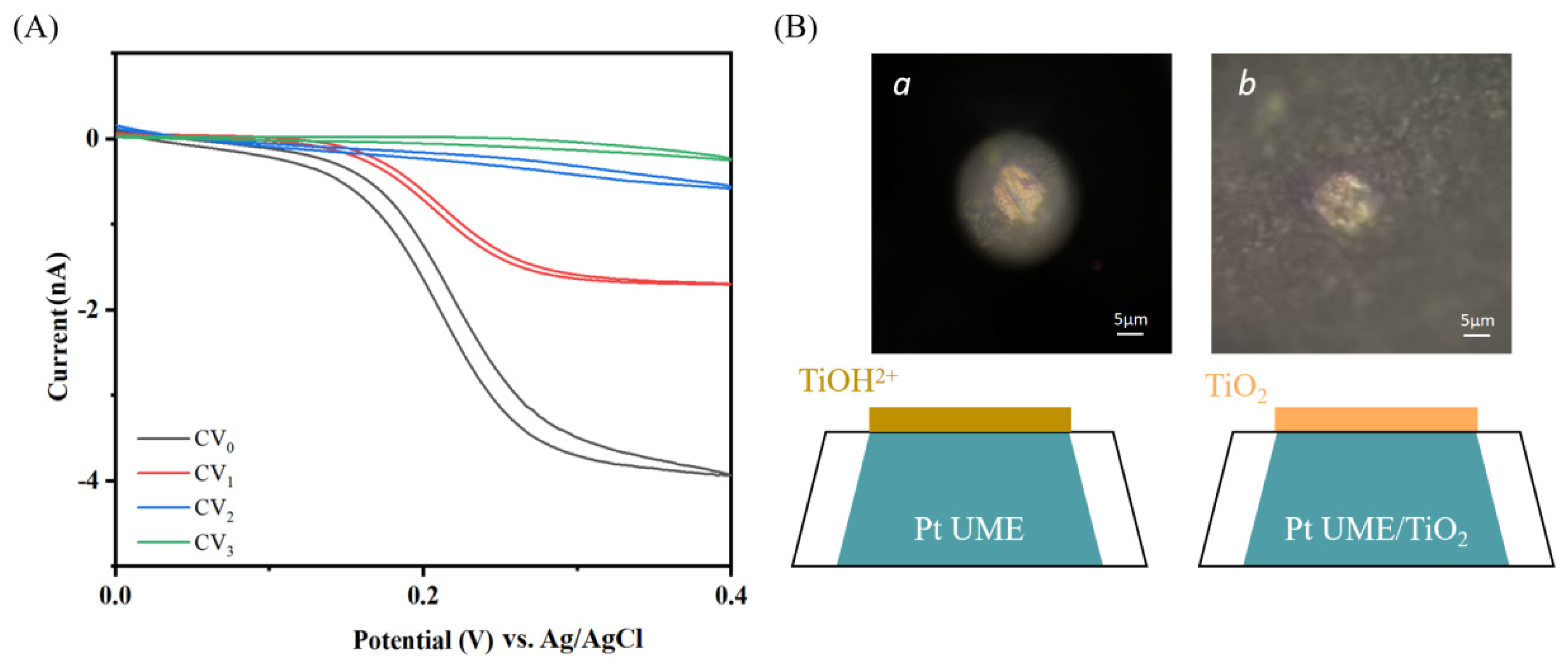
- II.
- A case of pinhole-free film electrodeposition on ultramicroelectrodes
4. Summary and Outlook
Author Contributions
Funding
Institutional Review Board Statement
Informed Consent Statement
Data Availability Statement
Conflicts of Interest
References
- Qiu, W.; Merckx, T.; Jaysankar, M.; Masse de la Huerta, C.; Rakocevic, L.; Zhang, W.; Paetzold, U.W.; Gehlhaar, R.; Froyen, L.; Poortmans, J.; et al. Pinhole-free perovskite films for efficient solar modules. Energy Environ. Sci. 2016, 9, 484–489. [Google Scholar] [CrossRef]
- Liang, Y.; Shang, Q.; Li, M.; Zhang, S.; Liu, X.; Zhang, Q. Solvent Recrystallization-Enabled Green Amplified Spontaneous Emissions with an Ultra-Low Threshold from Pinhole-Free Perovskite Films. Adv. Funct. Mater. 2021, 31, 2106108. [Google Scholar] [CrossRef]
- Nada, F.; Atta; Galal, A.; Amin, H.M.A. Synthesis and Photoelectrochemical Behavior of a Hybrid Electrode Composed of Polyaniline Encapsulated in Highly Ordered TiO2 Nanotubes Array. Int. J. Electrochem. Sci. 2012, 7, 3610–3626. [Google Scholar] [CrossRef]
- Zan, L.; Amin, H.M.A.; Mostafa, E.; Abd-El-Latif, A.A.; Iqbal, S.; Baltruschat, H. Electrodeposited Cobalt Nanosheets on Smooth Silver as a Bifunctional Catalyst for OER and ORR: In Situ Structural and Catalytic Characterization. ACS Appl. Mater. Interfaces 2022, 14, 55458–55470. [Google Scholar] [CrossRef]
- Kim, J.; Kim, B.-K.; Cho, S.K.; Bard, A.J. Tunneling Ultramicroelectrode: Nanoelectrodes and Nanoparticle Collisions. J. Am. Chem. Soc. 2014, 136, 8173–8176. [Google Scholar] [CrossRef]
- Atta, N.F.; Ahmed, R.A.; Amin, H.M.A.; Galal, A. Monodispersed Gold Nanoparticles Decorated Carbon Nanotubes as an Enhanced Sensing Platform for Nanomolar Detection of Tramadol. Electroanalysis 2012, 24, 2135–2146. [Google Scholar] [CrossRef]
- Amin, H.M.A.; El-Kady, M.F.; Atta, N.F.; Galal, A. Gold Nanoparticles Decorated Graphene as a High Performance Sensor for Determination of Trace Hydrazine Levels in Water. Electroanalysis 2018, 30, 1757–1766. [Google Scholar] [CrossRef]
- Xue, Z.; Zhu, Z.; Zhu, D.; Li, T.; Yang, C. High-speed electrodeposition of bright Cu with excellent mechanical properties utilizing friction of hard particles. J. Mater. Sci. 2023, 58, 3752–3767. [Google Scholar] [CrossRef]
- Bewick, A.; Fleischmann, M.; Thirsk, H.R. Kinetics of the electrocrystallization of thin films of calomel. Trans. Faraday Soc. 1962, 58, 2200–2216. [Google Scholar] [CrossRef]
- Avrami, M. Kinetics of Phase Change. I General Theory. J. Chem. Phys. 2004, 7, 1103–1112. [Google Scholar] [CrossRef]
- Avrami, M. Kinetics of Phase Change. II Transformation-Time Relations for Random Distribution of Nuclei. J. Chem. Phys. 2004, 8, 212–224. [Google Scholar] [CrossRef]
- Avrami, M. Granulation, Phase Change, and Microstructure Kinetics of Phase Change. III. J. Chem. Phys. 2004, 9, 177–184. [Google Scholar] [CrossRef]
- Scharifker, B.R.; Mostany, J. Three-dimensional nucleation with diffusion controlled growth: Part I. Number density of active sites and nucleation rates per site. J. Electroanal. Chem. Interfacial Electrochem. 1984, 177, 13–23. [Google Scholar] [CrossRef]
- Mostany, J.; Mozota, J.; Scharifker, B.R. Three-dimensional nucleation with diffusion controlled growth: Part II. The nucleation of lead on vitreous carbon. J. Electroanal. Chem. Interfacial Electrochem. 1984, 177, 25–37. [Google Scholar] [CrossRef]
- Scharifker, B.; Hills, G. Theoretical and experimental studies of multiple nucleation. Electrochim. Acta 1983, 28, 879–889. [Google Scholar] [CrossRef]
- Gunawardena, G.; Hills, G.; Montenegro, I.; Scharifker, B. Electrochemical nucleation: Part I. General considerations. J. Electroanal. Chem. Interfacial Electrochem. 1982, 138, 225–239. [Google Scholar] [CrossRef]
- Sluyters-Rehbach, M.; Wijenberg, J.H.O.J.; Bosco, E.; Sluyters, J.H. The theory of chronoamperometry for the investigation of electrocrystallization: Mathematical description and analysis in the case of diffusion-controlled growth. J. Electroanal. Chem. Interfacial Electrochem. 1987, 236, 1–20. [Google Scholar] [CrossRef]
- Heerman, L.; Matthijs, E.; Langerock, S. The concept of planar diffusion zones. Theory of the potentiostatic transient for multiple nucleation on active sites with diffusion-controlled growth. Electrochim. Acta 2001, 47, 905–911. [Google Scholar] [CrossRef]
- Mirkin, M.V.; Nilov, A.P. Three-dimensional nucleation and growth under controlled potential. J. Electroanal. Chem. Interfacial Electrochem. 1990, 283, 35–51. [Google Scholar] [CrossRef]
- Biswas, B.; Purandare, Y.; Sugumaran, A.A.; Loch, D.A.L.; Creasey, S.; Khan, I.; Ehiasarian, A.P.; Hovsepian, P.E. Defect growth in multilayer chromium nitride/niobium nitride coatings produced by combined high power impulse magnetron sputtering and unbalance magnetron sputtering technique. Thin Solid Film. 2017, 636, 558–566. [Google Scholar] [CrossRef]
- Vetter, J.; Stüber, M.; Ulrich, S. Growth effects in carbon coatings deposited by magnetron sputtering. Surf. Coat. Technol. 2003, 168, 169–178. [Google Scholar] [CrossRef]
- Lavrentieva, L.G.; Ivonin, I.V.; Krasilnikova, L.M.; Vilisova, M.D. Formation of submicron growth defects during vapour deposition of GaAs films. Kristall Technik 1980, 15, 683–689. [Google Scholar] [CrossRef]
- Mao, F.; Dong, C.; Macdonald, D.D. Effect of octadecylamine on the corrosion behavior of Type 316SS in acetate buffer. Corros. Sci. 2015, 98, 192–200. [Google Scholar] [CrossRef]
- Roelofs, L.D.; Chipkin, D.A.; Rockwell, C.J.; Behm, R.J. Mechanisms of hole formation in metal-on-metal epitaxial systems: Rh/Ag(001). Surf. Sci. 2003, 524, L89–L95. [Google Scholar] [CrossRef]
- de la Figuera, J.; Prieto, J.E.; Ocal, C.; Miranda, R. Surface etching and enhanced diffusion during the early stages of the growth of Co on Cu(111). Surf. Sci. 1994, 307–309, 538–543. [Google Scholar] [CrossRef]
- Klaua, M.; Höche, H.; Jenniches, H.; Barthel, J.; Kischner, J. Strain-driven formation of two-dimensional holes on Cu(111) after the deposition of Fe. Surf. Sci. 1997, 381, 106–116. [Google Scholar] [CrossRef]
- Ryland, R.G.; Hasegawa, S.; Williams, E.D. Silicon motion during antimony deposition on Si(111). Surf. Sci. 1996, 345, 222–234. [Google Scholar] [CrossRef]
- Scharifker, B.n.R.; Mostany, J.; Palomar-Pardavé, M.; González, I. On the Theory of the Potentiostatic Current Transient for Diffusion-Controlled Three-Dimensional Electrocrystallization Processes. J. Electrochem. Soc. 1999, 146, 1005. [Google Scholar] [CrossRef]
- Cao, Y.; West, A.C. Direct numerical simulation of nucleation and three-dimensional, diffusion-controlled growth on disk microelectrodes. J. Electroanal. Chem. 2001, 514, 103–108. [Google Scholar] [CrossRef]
- Miranda-Hernández, M.; González, I. Effect of Potential on the Early Stages of Nucleation and Growth during Silver Electrocrystallization in Ammonium Medium on Vitreous Carbon. J. Electrochem. Soc. 2004, 151, C220. [Google Scholar] [CrossRef]
- Madueño, R.; Pineda, T.; Sevilla, J.M.; Blázquez, M. Formation and Dissolution Processes of the 6-Thioguanine (6TG) Self-Assembled Monolayer. A Kinetic Study. J. Phys. Chem. B 2005, 109, 1491–1498. [Google Scholar] [CrossRef] [PubMed]
- Milchev, A.; Zapryanova, T. Nucleation and growth of copper under combined charge transfer and diffusion limitations: Part I. Electrochim. Acta 2006, 51, 2926–2933. [Google Scholar] [CrossRef]
- Milchev, A.; Zapryanova, T. Nucleation and growth of copper under combined charge transfer and diffusion limitations—Part II. Electrochim. Acta 2006, 51, 4916–4921. [Google Scholar] [CrossRef]
- Zapryanova, T.; Hrussanova, A.; Milchev, A. Nucleation and growth of copper on glassy carbon: Studies in extended overpotential interval. J. Electroanal. Chem. 2007, 600, 311–317. [Google Scholar] [CrossRef]
- Zapryanova, T.; Jordanov, N.; Milchev, A. Electrochemical growth of single copper crystals on glassy carbon and tungsten substrates. J. Electroanal. Chem. 2008, 612, 47–52. [Google Scholar] [CrossRef]
- Rezaei, M.; Tabaian, S.H.; Haghshenas, D.F. A kinetic description of Pd electrodeposition under mixed control of charge transfer and diffusion. J. Electroanal. Chem. 2012, 687, 95–101. [Google Scholar] [CrossRef]
- Altimari, P.; Pagnanelli, F. Electrochemical nucleation and three-dimensional growth under mixed kinetic-diffusion control: Analytical approximation of the current transient. Electrochim. Acta 2016, 205, 113–117. [Google Scholar] [CrossRef]
- Yuan, Y.; Luo, G.; Li, N. New in situ description of electrodepositing multiple nucleation processes under galvanostatic stimuli. RSC Adv. 2021, 11, 31526–31532. [Google Scholar] [CrossRef]
- Palomar-Pardavé, M.; Ramírez, M.T.; González, I.; Serruya, A.; Scharifker, B.R. Silver Electrocrystallization on Vitreous Carbon from Ammonium Hydroxide Solutions. J. Electrochem. Soc. 1996, 143, 1551–1558. [Google Scholar] [CrossRef]
- Altimari, P.; Pagnanelli, F. Electrochemical nucleation and three-dimensional growth of metal nanoparticles under mixed kinetic-diffusion control: Model development and validation. Electrochim. Acta 2016, 206, 116–126. [Google Scholar] [CrossRef]
- Chen, S.; Kucernak, A. Electrodeposition of Platinum on Nanometer-Sized Carbon Electrodes. J. Phys. Chem. B 2003, 107, 8392–8402. [Google Scholar] [CrossRef]
- Luo, G.; Li, D.; Yuan, G.; Li, N. Potentiostatic Current Transient for Multiple Nucleation: A Limited-Diffusion Process Description. J. Electrochem. Soc. 2018, 165, D147. [Google Scholar] [CrossRef]
- Fletcher, S. Some formulae describing spherical and hemispherical diffusion to small crystals in unstirred solutions. J. Cryst. Growth 1983, 62, 505–512. [Google Scholar] [CrossRef]
- Kruijt, W.S.; Sluyters-Rehbach, M.; Sluyters, J.H.; Milchev, A. Distribution of the nucleation rate in the vicinity of a growing spherical cluster.: Part 2. Theory of some special cases and experimental results. J. Electroanal. Chem. 1994, 371, 13–26. [Google Scholar] [CrossRef]
- Ustarroz, J.; Ke, X.X.; Hubin, A.; Bals, S.; Terryn, H. New Insights into the Early Stages of Nanoparticle Electrodeposition. J. Phys. Chem. C 2012, 116, 2322–2329. [Google Scholar] [CrossRef]
- Ustarroz, J.; Hammons, J.A.; Altantzis, T.; Hubin, A.; Bals, S.; Terryn, H. A Generalized Electrochemical Aggregative Growth Mechanism. J. Am. Chem. Soc. 2013, 135, 11550–11561. [Google Scholar] [CrossRef]
- Mamme, M.H.; Kohn, C.; Deconinck, J.; Ustarroz, J. Numerical insights into the early stages of nanoscale electrodeposition: Nanocluster surface diffusion and aggregative growth. Nanoscale 2018, 10, 7194–7209. [Google Scholar] [CrossRef]
- Arbib, M.; Zhang, B.; Lazarov, V.; Stoychev, D.; Milchev, A.; Buess-Herman, C. Electrochemical nucleation and growth of rhodium on gold substrates. J. Electroanal. Chem. 2001, 510, 67–77. [Google Scholar] [CrossRef]
- Thirsk, H.R.; Harrison, J.A. A Guide to the Study of Electrode Kinetics; Academic Press: Cambridge, MA, USA, 1972. [Google Scholar]
- Altimari, P.; Schiavi, P.G.; Rubino, A.; Pagnanelli, F. Electrodeposition of cobalt nanoparticles: An analysis of the mechanisms behind the deviation from three-dimensional diffusion-control. J. Electroanal. Chem. 2019, 851, 113413. [Google Scholar] [CrossRef]
- Schulz, E.N.; Ruderman, A.; Soldano, G.J.; García, S.G.; Santos, E. Key role of anions in the 2D–3D electrochemical deposition of Rh on Ag electrodes. Electrochim. Acta 2015, 178, 813–822. [Google Scholar] [CrossRef]
- Kibler, L.A.; Kleinert, M.; Kolb, D.M. The initial stages of rhodium deposition on Au(111). J. Electroanal. Chem. 1999, 467, 249–257. [Google Scholar] [CrossRef]
- Grdeń, M.; Próchniak, M. Electrode Surface Coverage with Deposit Generated Under Conditions of Electrochemical Nucleation and Growth. A Mathematical Analysis. Electrocatalysis 2023, 14, 39–54. [Google Scholar] [CrossRef]
- Palomar-Pardavé, M.; Miranda-Hernández, M.; González, I.; Batina, N. Detailed characterization of potentiostatic current transients with 2D-2D and 2D-3D nucleation transitions. Surf. Sci. 1998, 399, 80–95. [Google Scholar] [CrossRef]
- Medrano-Banda, A.; Crespo-Yapur, A.; Velasco-Soto, M.Á.; Videa, M. Galvanostatically Deposited PtNi Thin-Films as Electrocatalysts for the Hydrogen Evolution Reaction. ChemistryOpen 2022, 11, e202100241. [Google Scholar] [CrossRef] [PubMed]
- Rafiee, M.; Mayer, M.N.; Punchihewa, B.T.; Mumau, M.R. Constant Potential and Constant Current Electrolysis: An Introduction and Comparison of Different Techniques for Organic Electrosynthesis. J. Org. Chem. 2021, 86, 15866–15874. [Google Scholar] [CrossRef]
- Hörmann, N.G.; Beinlich, S.D.; Reuter, K. Converging Divergent Paths: Constant Charge vs Constant Potential Energetics in Computational Electrochemistry. J. Phys. Chem. C 2024, 128, 5524–5531. [Google Scholar] [CrossRef]
- Rasche, B.; Amin, H.M.A.; Clarke, S.J.; Compton, R.G. Polyselenides on the route to electrodeposited selenium. J. Electroanal. Chem. 2019, 835, 239–247. [Google Scholar] [CrossRef]
- Jadhav, H.S.; Kalubarme, R.S.; Ahn, S.; Yun, J.H.; Park, C.-J. Effects of duty cycle on properties of CIGS thin films fabricated by pulse-reverse electrodeposition technique. Appl. Surf. Sci. 2013, 268, 391–396. [Google Scholar] [CrossRef]
- Wang, X.; Ye, X.; Zhang, L.; Shao, Y.; Zhou, X.; Lu, M.; Chu, C.; Xue, F.; Bai, J. Corrosion and antimicrobial behavior of stainless steel prepared by one-step electrodeposition of silver at the grain boundaries. Surf. Coat. Technol. 2022, 439, 128428. [Google Scholar] [CrossRef]
- Lara-Lara, B.; Fernández, A.M. Growth improved of CIGS thin films by applying mechanical perturbations to the working electrode during the electrodeposition process. Superlattices Microstruct. 2019, 128, 144–150. [Google Scholar] [CrossRef]
- Biswal, H.J.; Vundavilli, P.R.; Gupta, A.J.J.o.T.E.S. Perspective—Electrodeposition of Graphene Reinforced Metal Matrix Composites for Enhanced Mechanical and Physical Properties: A Review. J. Electrochem. Soc. 2020, 167, 146501. [Google Scholar] [CrossRef]
- Mariani, E.; Giurlani, W.; Bonechi, M.; Dell’Aquila, V.; Innocenti, M. A systematic study of pulse and pulse reverse plating on acid copper bath for decorative and functional applications. Sci. Rep. 2022, 12, 18175. [Google Scholar] [CrossRef] [PubMed]
- Guo, L.; Searson, P.C. On the influence of the nucleation overpotential on island growth in electrodeposition. Electrochim. Acta 2010, 55, 4086–4091. [Google Scholar] [CrossRef]
- Komsiyska, L.; Staikov, G. Electrocrystallization of Au nanoparticles on glassy carbon from HClO4 solution containing [AuCl4]−. Electrochim. Acta 2008, 54, 168–172. [Google Scholar] [CrossRef]
- Bayati, M.; Abad, J.M.; Nichols, R.J.; Schiffrin, D.J. Substrate Structural Effects on the Synthesis and Electrochemical Properties of Platinum Nanoparticles on Highly Oriented Pyrolytic Graphite. J. Phys. Chem. C 2010, 114, 18439–18448. [Google Scholar] [CrossRef]
- Isaev, V.A.; Grishenkova, O.V.; Zaykov, Y.P. On the theory of 3D multiple nucleation with kinetic controlled growth. J. Electroanal. Chem. 2018, 818, 265–269. [Google Scholar] [CrossRef]
- Li, H.; Zhang, X.; Sun, Z.; Ma, W. Rapid Screening of Bimetallic Electrocatalysts Using Single Nanoparticle Collision Electrochemistry. J. Am. Chem. Soc. 2022, 144, 16480–16489. [Google Scholar] [CrossRef]
- Natter, H.; Hempelmann, R.J.C. Nanocrystalline Copper by Pulsed Electrodeposition: The Effects of Organic Additives, Bath Temperature, and pH. J. Phys. Chem. 1997, 100, 19525–19532. [Google Scholar] [CrossRef]
- Chandrasekar, M.S.; Pushpavanam, M. Pulse and pulse reverse plating—Conceptual, advantages and applications. Electrochim. Acta 2008, 53, 3313–3322. [Google Scholar] [CrossRef]
- Ren, X.; Qi, Y.; Li, Y.; Zhou, J.; Wang, B.; Li, J. Electrodeposition of tungsten coatings and deuterium irradiation behavior of tungsten coatings. J. Mater. Sci. 2022, 57, 10118–10128. [Google Scholar] [CrossRef]
- Dhara, T.; Aryanfar, A.; Ghosh, A.; Ghosh, U.; Mukherjee, P.; DasGupta, S. The Role of Pulse Duty Cycle and Frequency on Dendritic Compression. J. Phys. Chem. C 2023, 127, 4407–4415. [Google Scholar] [CrossRef]
- Ouyang, Y.; Zhang, Z.; Huang, W.; Yang, W.; Shen, C.; Chen, Y.; Yin, X.; Liu, Y. Electrodeposition of F-doped hydroxyapatite-TiO2 coating on AZ31 magnesium alloy for enhancing corrosion protection and biocompatibility. J. Mater. Sci. 2022, 57, 17188–17202. [Google Scholar] [CrossRef]
- Slade, P.G. Electrical Contacts: Principles and Applications, 2nd ed.; CRC Press: Boca Raton, FL, USA, 2014; pp. 132–133, 197–198. [Google Scholar]
- Singha Roy, S.; Jacobberger, R.M.; Wan, C.; Arnold, M.S. Controlling the density of pinhole defects in monolayer graphene synthesized via chemical vapor deposition on copper. Carbon 2016, 100, 1–6. [Google Scholar] [CrossRef]
- Ji, X.; Song, L.; He, W.; Huang, K.; Yan, Z.; Zhong, S.; Zhang, Y.; Zhao, R.A.-O. Super Nonlinear Electrodeposition-Diffusion-Controlled Thin-Film Selector. ACS Appl. Mater. Interfaces 2018, 10, 10165–10172. [Google Scholar] [CrossRef]
- Silván, B.; Gonzalo, E.; Djuandhi, L.; Sharma, N.; Fauth, F.; Saurel, D. On the dynamics of transition metal migration and its impact on the performance of layered oxides for sodium-ion batteries: NaFeO2 as a case study. J. Mater. Chem. A 2018, 6, 15132–15146. [Google Scholar] [CrossRef]
- Liu, J.; Du, Z.; Wang, X.; Tan, S.; Wu, X.; Geng, L.; Song, B.; Chien, P.-H.; Everett, S.M.; Hu, E. Anionic redox induced anomalous structural transition in Ni-rich cathodes. Energy Environ. Sci. 2021, 14, 6441–6454. [Google Scholar] [CrossRef]
- Chang, S.L.; Wen, J.M.; Thiel, P.A.; Gunther, S.; Meyer, J.A.; Behm, R.J. Initial stages of metal encapsulation during epitaxial growth studied by STM: Rh/Ag(100). Phys. Rev. B 1996, 53, 13747–13752. [Google Scholar] [CrossRef]
- Belousov, I.V.; Grib, A.N.; Kuznetsov, G.V. The influence of surface defects on the pinhole formation in silicide thin film. Semicond. Phys. Quantum Electron. Optoelectron. 2006, 9, 29–34. [Google Scholar] [CrossRef]
- Su, T.-S.; Hsieh, T.-Y.; Hong, C.-Y.; Wei, T.-C. Electrodeposited Ultrathin TiO2 Blocking Layers for Efficient Perovskite Solar Cells. Sci. Rep. 2015, 5, 16098. [Google Scholar] [CrossRef]
- Trevethan, T.; Latham, C.D.; Heggie, M.I.; Briddon, P.R.; Rayson, M.J. Vacancy diffusion and coalescence in graphene directed by defect strain fields. Nanoscale 2014, 6, 2978–2986. [Google Scholar] [CrossRef]
- Colombara, D.; Elanzeery, H.; Nicoara, N.; Sharma, D.; Claro, M.; Schwarz, T.; Koprek, A.; Wolter, M.H.; Melchiorre, M.; Sood, M.; et al. Chemical instability at chalcogenide surfaces impacts chalcopyrite devices well beyond the surface. Nat. Commun. 2020, 11, 3634. [Google Scholar] [CrossRef] [PubMed]
- Wu, L.; Hou, T.; Li, Y.; Chan, K.; Lee, S.-T. First-Principles Study on Migration and Coalescence of Point Defects in Monolayer Graphene. J. Phys. Chem. C 2013, 117, 17066–17072. [Google Scholar] [CrossRef]
- Zhang, H.; Zhao, M.; Yang, X.; Xia, H.; Liu, X.; Xia, Y. Diffusion and coalescence of vacancies and interstitials in graphite: A first-principles study. Diam. Relat. Mater. 2010, 19, 1240–1244. [Google Scholar] [CrossRef]
- Abadias, G.; Chason, E.; Keckes, J.; Sebastiani, M.; Thompson, G.B.; Barthel, E.; Doll, G.L.; Murray, C.E.; Stoessel, C.H.; Martinu, L. Review Article: Stress in thin films and coatings: Current status, challenges, and prospects. J. Vac. Sci. Technol. A 2018, 36, 020801. [Google Scholar] [CrossRef]
- Dolabella, S.; Borzì, A.; Dommann, A.; Neels, A. Lattice Strain and Defects Analysis in Nanostructured Semiconductor Materials and Devices by High-Resolution X-Ray Diffraction: Theoretical and Practical Aspects. Small Methods 2022, 6, 2100932. [Google Scholar] [CrossRef]
- Yoon, J.K.; Jung, G.-E.; Kim, H.; Chung, K.H.; Kahng, S.-J. Two-dimensional vacancy islands induced by the growth of Cr on Cu(111). Thin Solid Film. 2010, 519, 1375–1379. [Google Scholar] [CrossRef]
- Shorinov, O. Tensile Stress as a Factor of Deformation and Failure of Thin Films and Coatings. In Integrated Computer Technologies in Mechanical Engineering—2021; Nechyporuk, M., Pavlikov, V., Kritskiy, D., Eds.; Springer International Publishing: Cham, Switzerland, 2022; pp. 26–35. [Google Scholar]
- Shugurov, A.R.; Panin, A.V. Mechanisms of Stress Generation in Thin Films and Coatings. Tech. Phys. 2020, 65, 1881–1904. [Google Scholar] [CrossRef]
- Nikolić, N.D.; Pavlović, L.J.; Pavlović, M.G.; Popov, K.I. Formation of dish-like holes and a channel structure in electrodeposition of copper under hydrogen co-deposition. Electrochim. Acta 2007, 52, 8096–8104. [Google Scholar] [CrossRef]
- Nikolić, N.D.; Popov, K.I. Hydrogen Co-deposition Effects on the Structure of Electrodeposited Copper. In Electrodeposition: Theory and Practice; Djokic, S.S., Ed.; Springer: New York, NY, USA, 2010; pp. 1–70. [Google Scholar]
- Shin, H.-C.; Dong, J.; Liu, M. Porous Tin Oxides Prepared Using an Anodic Oxidation Process. Adv. Mater. 2004, 16, 237–240. [Google Scholar] [CrossRef]
- Mendoza-Huizar, L.H.; Rios-Reyes, C.H. Cobalt electrodeposition onto polycrystalline gold from ammoniacal solutions. Cent. Eur. J. Chem. 2013, 11, 1381–1392. [Google Scholar] [CrossRef]
- Zech, N.; Landolt, D. The influence of boric acid and sulfate ions on the hydrogen formation in Ni Fe plating electrolytes. Electrochim. Acta 2000, 45, 3461–3471. [Google Scholar] [CrossRef]
- Guo, L.; Oskam, G.; Radisic, A.; Hoffmann, P.; Searson, P. Island growth in electrodeposition. J. Phys. D Appl. Phys. 2011, 44, 443001. [Google Scholar] [CrossRef]
- Li, Z.; Luo, L.; Li, M.; Chen, W.; Liu, Y.; Yang, J.; Xu, S.-M.; Zhou, H.; Ma, L.; Xu, M.; et al. Photoelectrocatalytic C–H halogenation over an oxygen vacancy-rich TiO2 photoanode. Nat. Commun. 2021, 12, 6698. [Google Scholar] [CrossRef] [PubMed]
- Guo, L.; Thompson, A.; Searson, P.C. The kinetics of copper island growth on ruthenium oxide in perchlorate solution. Electrochim. Acta 2010, 55, 8416–8421. [Google Scholar] [CrossRef]
- Besson, C.; Finney, E.E.; Finke, R.G. A Mechanism for Transition-Metal Nanoparticle Self-Assembly. J. Am. Chem. Soc. 2005, 127, 8179–8184. [Google Scholar] [CrossRef]
- Zhang, P.; Xu, Z.; Meng, G.; Wang, Y.; Wang, J.; Shao, Y.; Wang, F. Efficiently Improved Corrosion Resistance of Electrodeposition Ni–Cu Coatings via Site-Blocking Effect of Ce. Adv. Eng. Mater. 2022, 24, 2200109. [Google Scholar] [CrossRef]
- Kaneko, Y.; Hiwatari, Y.; Ohara, K.; Murakami, T. Monte Carlo Simulation of Thin Film Growth with Lattice Defects. J. Phys. Soc. Jpn. 2000, 69, 3607–3613. [Google Scholar] [CrossRef]
- Ahn, H.S.; Bard, A.J. Single-Nanoparticle Collision Events: Tunneling Electron Transfer on a Titanium Dioxide Passivated n-Silicon Electrode. Angew. Chem. -Int. Ed. 2015, 54, 13753–13757. [Google Scholar] [CrossRef]
- Deheryan, S.; Cott, D.J.; Muller, R.; Timmermans, M.; Heyns, M.; Vereecken, P.M. Self-limiting electropolymerization of ultrathin, pinhole-free poly(phenylene oxide) films on carbon nanosheets. Carbon 2015, 88, 42–50. [Google Scholar] [CrossRef]
- Wang, A.; Ornelas, C.; Astruc, D.; Hapiot, P. Electronic Communication between Immobilized Ferrocenyl-Terminated Dendrimers. J. Am. Chem. Soc. 2009, 131, 6652–6653. [Google Scholar] [CrossRef]
- Tevi, T.; Yaghoubi, H.; Wang, J.; Takshi, A. Application of poly (p-phenylene oxide) as blocking layer to reduce self-discharge in supercapacitors. J. Power Sources 2013, 241, 589–596. [Google Scholar] [CrossRef]
- Amegroud, H.; Boudalia, M.; Elhawary, M.; Garcia, A.J.; Bellaouchou, A.; Amin, H.M.A. Electropolymerized conducting polyaniline coating on nickel-aluminum bronze alloy for improved corrosion resistance in marine environment. Colloids Surf. A Physicochem. Eng. Asp. 2024, 691, 133909. [Google Scholar] [CrossRef]
- Das, R.; Chanda, A. Fabrication and Properties of Spin-Coated Polymer Films. In Nano-Size Polymers: Preparation, Properties, Applications; Fakirov, S., Ed.; Springer International Publishing: Cham, Switzerland, 2016; pp. 283–306. [Google Scholar]
- Xu, H.; Yan, W.; Tang, C.L. A novel method to prepare metal oxide electrode: Spin-coating with thermal decomposition. Chin. Chem. Lett. 2011, 22, 354–357. [Google Scholar] [CrossRef]
- Chakraborty, A.; Herrera, D.; Fallen, P.; Hall, D.; Bampton, N.; Olivero, T.; Orlowski, M. Conductive organic electrodes for flexible electronic devices. Sci. Rep. 2023, 13, 4125. [Google Scholar] [CrossRef] [PubMed]
- Sharma, A.; Masoumi, S.; Gedefaw, D.; O’Shaughnessy, S.; Baran, D.; Pakdel, A. Flexible solar and thermal energy conversion devices: Organic photovoltaics (OPVs), organic thermoelectric generators (OTEGs) and hybrid PV-TEG systems. Appl. Mater. Today 2022, 29, 101614. [Google Scholar] [CrossRef]
- Workie, A.B.; Ningsih, H.S.; Shih, S.-J. An comprehensive review on the spray pyrolysis technique: Historical context, operational factors, classifications, and product applications. J. Anal. Appl. Pyrolysis 2023, 170, 105915. [Google Scholar] [CrossRef]
- Shih, S.-J.; Tzeng, W.-L.; Kuo, W.-L. Fabrication of ceria particles using glycine nitrate spray pyrolysis. Surf. Coat. Technol. 2014, 259, 302–309. [Google Scholar] [CrossRef]
- Shih, S.-J.; Chien, I.C. Preparation and characterization of nanostructured silver particles by one-step spray pyrolysis. Powder Technol. 2013, 237, 436–441. [Google Scholar] [CrossRef]
- Li, Z.; Su, J.; Wang, X. Atomic layer deposition in the development of supercapacitor and lithium-ion battery devices. Carbon 2021, 179, 299–326. [Google Scholar] [CrossRef]
- Riyanto, E.; Martides, E.; Pikra, G.; Atmaja, T.D.; Pramana, R.I.; Purwanto, A.J.; Santosa, A.; Junianto, E.; Darussalam, R.; Saepudin, A.; et al. A review of atomic layer deposition for high lithium-ion battery performance. J. Mater. Res. Technol. 2021, 15, 5466–5481. [Google Scholar] [CrossRef]
- Neudeck, S.; Mazilkin, A.; Reitz, C.; Hartmann, P.; Janek, J.; Brezesinski, T. Effect of Low-Temperature Al2O3 ALD Coating on Ni-Rich Layered Oxide Composite Cathode on the Long-Term Cycling Performance of Lithium-Ion Batteries. Sci. Rep. 2019, 9, 5328. [Google Scholar] [CrossRef] [PubMed]
- Mariella Babu, A.; Varghese, A. Electrochemical deposition for metal organic Frameworks: Advanced Energy, Catalysis, sensing and separation applications. J. Electroanal. Chem. 2023, 937, 117417. [Google Scholar] [CrossRef]
- Krysova, H.; Zlamalova, M.; Tarabkova, H.; Jirkovsky, J.; Frank, O.; Kohout, M.; Kavan, L. Rutile TiO2 thin film electrodes with excellent blocking function and optical transparency. Electrochim. Acta 2019, 321, 134685. [Google Scholar] [CrossRef]
- Wang, L.; Wang, M.; Zhong, M.; Li, X.; Cui, Z. Degradation of thermal oxide film on pure titanium in an acidic environment containing fluoride. Npj Mater. Degrad. 2022, 6, 65. [Google Scholar] [CrossRef]
- Hong, S.; Han, A.; Lee, E.C.; Ko, K.-W.; Park, J.-H.; Song, H.-J.; Han, M.-H.; Han, C.-H. A facile and low-cost fabrication of TiO2 compact layer for efficient perovskite solar cells. Curr. Appl. Phys. 2015, 15, 574–579. [Google Scholar] [CrossRef]
- Su, T.S.; Hsieh, T.Y.; Wei, T.C. Electrodeposited TiO2 Film with Mossy Nanostructure for Efficient Compact Layer in Scaffold-Type Perovskite Solar Cell. Sol. RRL 2018, 2, 1700120. [Google Scholar] [CrossRef]
- Jang, K.-I.; Hong, E.; Kim, J.H. Effect of an electrodeposited TiO2 blocking layer on efficiency improvement of dye-sensitized solar cell. Korean J. Chem. Eng. 2012, 29, 356–361. [Google Scholar] [CrossRef]
- Zhang, Z.; Feng, C.; Liu, C.; Zuo, M.; Qin, L.; Yan, X.; Xing, Y.; Li, H.; Si, R.; Zhou, S.; et al. Electrochemical deposition as a universal route for fabricating single-atom catalysts. Nat. Commun. 2020, 11, 1215. [Google Scholar] [CrossRef]
- Sheng, X.; Zeng, Z.; Du, C.; Shu, T.; Meng, X. Amorphous porous germanium anode with variable dimension for lithium ion batteries. J. Mater. Sci. 2021, 56, 15258–15267. [Google Scholar] [CrossRef]
- Hu, W.; Yang, S.; Yang, S. Surface Modification of TiO2 for Perovskite Solar Cells. Trends Chem. 2020, 2, 148–162. [Google Scholar] [CrossRef]
- Anuratha, K.S.; Peng, H.-S.; Xiao, Y.; Su, T.-S.; Wei, T.-C.; Lin, J.-Y. Electrodeposition of nanostructured TiO2 thin film as an efficient bifunctional layer for perovskite solar cells. Electrochim. Acta 2019, 295, 662–667. [Google Scholar] [CrossRef]
- Hussin, R.; Choy, K.L.; Hou, X.H. Growth of TiO2 Thin Films by Atomic Layer Deposition (ALD). Adv. Mater. Res. 2016, 1133, 352–356. [Google Scholar] [CrossRef]
- Shalan, A.; Narra, S.; Oshikiri, T.; Ueno, K.; Shi, X.; Wu, H.-P.; Elshanawany, M.; Diau, E.; Misawa, H. Optimization of a Compact Layer of TiO2 via Atomic-layer Deposition for High-performance Perovskite Solar Cells. Sustain. Energy Fuels 2017, 1, 1533–1540. [Google Scholar] [CrossRef]
- Zhou, B.; Jiang, X.; Liu, Z.; Shen, R.; Rogachev, A.V. Preparation and characterization of TiO2 thin film by thermal oxidation of sputtered Ti film. Mater. Sci. Semicond. Process. 2013, 16, 513–519. [Google Scholar] [CrossRef]
- Zhu, Z.; Liu, X.; Ye, Z.; Zhang, J.; Cao, F.; Zhang, J. A fabrication of iridium oxide film pH micro-sensor on Pt ultramicroelectrode and its application on in-situ pH distribution of 316L stainless steel corrosion at open circuit potential. Sens. Actuators B Chem. 2018, 255, 1974–1982. [Google Scholar] [CrossRef]
- Zeng, Q.; Xia, K.; Zhang, Y.; Wu, T. Well Controlled 3D Iridium Oxide/Platinum Nanocomposites with Greatly Enhanced Electrochemical Performances. Adv. Mater. Interfaces 2019, 6, 1900356. [Google Scholar] [CrossRef]
- Lee, S.A.; Yang, J.W.; Choi, S.; Jang, H.W. Nanoscale electrodeposition: Dimension control and 3D conformality. Exploration 2021, 1, 20210012. [Google Scholar] [CrossRef]
- Adams, R.N. Probing brain chemistry with electroanalytical techniques. Anal. Chem. 1976, 48, 1126A–1138A. [Google Scholar] [CrossRef]
- Kavan, L.; O’Regan, B.; Kay, A.; Grätzel, M. Preparation of TiO2 (anatase) films on electrodes by anodic oxidative hydrolysis of TiCl3. J. Electroanal. Chem. 1993, 346, 291–307. [Google Scholar] [CrossRef]
- Chi, B.; Li, J.; Yang, X.; Gong, Y.; Wang, N. Deposition of Ni–Co by cyclic voltammetry method and its electrocatalytic properties for oxygen evolution reaction. Int. J. Hydrogen Energy 2005, 30, 29–34. [Google Scholar] [CrossRef]
- Bai, A.; Hu, C.-C. Effects of electroplating variables on the composition and morphology of nickel–cobalt deposits plated through means of cyclic voltammetry. Electrochim. Acta 2002, 47, 3447–3456. [Google Scholar] [CrossRef]
- Chen, Y.; Yang, H.; Feng, H.; Yang, P.; Zhang, J.; Shu, B. Electrodeposition and corrosion performance of Ni-Co alloys with different cobalt contents. Mater. Today Commun. 2023, 35, 106058. [Google Scholar] [CrossRef]
- Pandit, B.; Goda, E.S.; Shaikh, S.F. Electrochemical Deposition Toward Thin Films. In Simple Chemical Methods for Thin Film Deposition: Synthesis and Applications; Sankapal, B.R., Ennaoui, A., Gupta, R.B., Lokhande, C.D., Eds.; Springer Nature: Singapore, 2023; pp. 245–304. [Google Scholar]
- Hyde, M.E.; Compton, R.G. A review of the analysis of multiple nucleation with diffusion controlled growth. J. Electroanal. Chem. 2003, 549, 1–12. [Google Scholar] [CrossRef]


Disclaimer/Publisher’s Note: The statements, opinions and data contained in all publications are solely those of the individual author(s) and contributor(s) and not of MDPI and/or the editor(s). MDPI and/or the editor(s) disclaim responsibility for any injury to people or property resulting from any ideas, methods, instructions or products referred to in the content. |
© 2024 by the authors. Licensee MDPI, Basel, Switzerland. This article is an open access article distributed under the terms and conditions of the Creative Commons Attribution (CC BY) license (https://creativecommons.org/licenses/by/4.0/).
Share and Cite
Gao, Z.; Jiang, Y.; Meng, Y.; Du, M.; Liu, F. A Review of the Fabrication of Pinhole-Free Thin Films Based on Electrodeposition Technology: Theory, Methods and Progress. Molecules 2024, 29, 5615. https://doi.org/10.3390/molecules29235615
Gao Z, Jiang Y, Meng Y, Du M, Liu F. A Review of the Fabrication of Pinhole-Free Thin Films Based on Electrodeposition Technology: Theory, Methods and Progress. Molecules. 2024; 29(23):5615. https://doi.org/10.3390/molecules29235615
Chicago/Turabian StyleGao, Zike, Yuze Jiang, Yao Meng, Minshu Du, and Feng Liu. 2024. "A Review of the Fabrication of Pinhole-Free Thin Films Based on Electrodeposition Technology: Theory, Methods and Progress" Molecules 29, no. 23: 5615. https://doi.org/10.3390/molecules29235615
APA StyleGao, Z., Jiang, Y., Meng, Y., Du, M., & Liu, F. (2024). A Review of the Fabrication of Pinhole-Free Thin Films Based on Electrodeposition Technology: Theory, Methods and Progress. Molecules, 29(23), 5615. https://doi.org/10.3390/molecules29235615