Article

Preparation of Surface Dispersed WO3/BiVO4 Heterojunction Arrays and Their Photoelectrochemical Performance for Water Splitting

1
Jiangsu Key Laboratory of Advanced Structural Materials and Application Technology, School of Materials Science and Engineering, Nanjing Institute of Technology, Nanjing 211167, China
2
College of Materials Science and Technology, Nanjing University of Aeronautics and Astronautics, Nanjing 210016, China
3
School of Environmental Science and Engineering, Nanjing University of Information Science & Technology, Nanjing 210044, China
*
Authors to whom correspondence should be addressed.
Molecules 2024, 29(2), 372; https://doi.org/10.3390/molecules29020372
Submission received: 12 November 2023 / Revised: 29 December 2023 / Accepted: 8 January 2024 / Published: 11 January 2024
(This article belongs to the Special Issue Nanomaterials for Energy Storage and Conversion)

Abstract

:
In this work, a surface dispersed heterojunction of BiVO4-nanoparticle@WO3-nanoflake was successfully prepared by hydrothermal combined with solvothermal method. We optimized the morphology of the WO3 nanoflakes and BiVO4 nanoparticles by controlling the synthesis conditions to get the uniform BiVO4 loaded on the surface of WO3 arrays. The phase composition and morphology evolution with different reaction precursors were investigated in detail. When used as photoanodes, the WO3/BiVO4 composite exhibits superior activity with photocurrent at 3.53 mA cm−2 for photoelectrochemical (PEC) water oxidation, which is twice that of pure WO3 photoanode. The superior surface dispersion structure of the BiVO4-nanoparticle@WO3-nanoflake heterojunction ensures a large effective heterojunction area and relieves the interfacial hole accumulation at the same time, which contributes to the improved photocurrents together with the stability of the WO3/BiVO4 photoanodes.

1. Introduction

Photoelectrochemical (PEC) water splitting provides a promising strategy to relieve global energy demands and environmental problems as it can harvest solar energy and convert it into chemical energy in the form of a reaction product of hydrogen [1,2,3,4]. In a PEC system, the photoanode, where the oxygen evolution reaction (OER) takes place, suffers from sluggish kinetics and appears to be a rate-limiting step [5,6]. It is of great significance to searching for effective photoanodes.
Among the promising photoanode materials, WO3, which is featured with electron mobility of 10 cm2 V−1 s−1, electron diffusion length of ~500 nm and hole diffusion distance of ~150 nm [7,8], has significant advantages in charge carrier transport characteristics over other common semiconductors, such as TiO2 [9,10,11], ZnO [12,13] and α-Fe2O3 [14,15,16]. However, although WO3 can respond to visible light to some extent, the large band gap still leads to limited visible light absorption [17,18]. Thus, the theoretical solar to hydrogen (STH) efficiency of WO3 is only about 4.5% [19]. BiVO4 possesses a narrow band gap of ~2.4 eV, which can absorb a large part of the visible light with the wavelength below 520 nm [20,21]. The band gap determines that the maximum theoretical water oxidation photocurrent of BiVO4 photoanode is 7.5 mA cm−2 under standard solar radiation (AM 1.5 G) and STH efficiency is close to 9.2% [22]. In addition, BiVO4 has the advantages of light corrosion resistance. However, the electron mobility of BiVO4 is poor [20], which causes an imbalance between the efficiency of light harvest and charge separation in BiVO4. This is the bottleneck of BiVO4 photoanodes.
It has been reported that the construction of the WO3/BiVO4 heterojunction can integrate the advantages of WO3 and BiVO4, where WO3 can serve as carrier conduction layer and BiVO4 as the main absorber toward visible light [23,24,25]. As a result, the heterojunction can not only widen the range of light utilization, but also promote the effective charge separation [26]. In 2011, Suk Joon Hong et al. first prepared a series of WO3/BiVO4 heterojunctions with different WO3 or BiVO4 thicknesses, and it was reported that the obtained photocurrents were closely related to the WO3/BiVO4 structure [27]. From then, new structures of WO3/BiVO4 heterojunctions were further developed, such as 1D nanorod core-shell [28,29], 2D nanosheet core-shell [30] and 3D inverse opal structures [31,32]. However, the structural optimization mainly focused on the morphology and pore distribution of the underlying WO3; there are still few reports on the upper BiVO4 layer. Most studies reported the WO3/BiVO4 heterojunction adopting the spin or drop coating to deposit a conformal BiVO4 layer onto the WO3 [33,34,35,36,37,38]. However, this process is complex and needs repeated coating and annealing. Moreover, it often gives a non-uniform coating layer on the surface of WO3.
It has been reported that there are mainly three kinds of heterojunction configurations: (1) the planar laminations, which can be easily prepared by combining different semiconductor layers, but the planar structure severely limits the active area of electrodes; (2) the core-shell coaxial structure, which can significantly improve the effective heterojunction area, but the holes generated by the inner semiconductor can only be transmitted to the surface semiconductor through the heterojunction, which might lead to the accumulation of charge carriers at the semiconductor interface; and (3) the surface dispersion structure, which can ensure that both kinds of semiconductor can accept light and participate in the surface reaction, and at the same time remaining a large effective heterojunction area. Therefore, to fabricate the surface dispersed WO3/BiVO4 heterojunction arrays shows great potential to improve its performance toward PEC water oxidation. Hyungtak Seo et al. [39] used ethyl cellulose as the morphology control agent and prepared BiVO4 with island morphology decorated on the WO3 layer via the spin coating. Ho Won Jang et al. [40] prepared dot-like BiVO4 coated on the entire surface of WO3 nanorods by pulse electrodeposition, which could significantly increase the active area of the heterojunction. Kiyoung Lee et al. [41] investigated the interfacial growth of the optimal BiVO4 nanoparticles onto WO3 nanoplates via a chemical bath deposition method; however, it still could not avoid the ten times of repeated coating procedure. Hongbing Yu et al. [42] synthesized the coral-like WO3/BiVO4 photoanode via BiOI electrodeposition with a relatively complex process. Huixia Guo et al. [43] reported the synthesis of BiVO4 nanoparticles on the WO3 thin film by hydrothermal method; however, the structure still needs to be optimized to decrease the particle agglomeration.
In this work, the surface dispersed heterojunction structure of BiVO4-nanoparticle@WO3-nanoflake was prepared by the hydrothermal combined with solution-thermal method to obtain high PEC water splitting performance. Firstly, WO3 nanoflake arrays with optimized properties were obtained by changing the synthesis conditions and controlling the morphology of WO3 films by hydrothermal method. Afterwards, uniform BiVO4 nanoparticles were covered on the surface of WO3 nanoflake arrays through the secondary solvothermal process. As a result of the formation of WO3/BiVO4 heterojunction and its well-arranged structure, the performance of the surface dispersed WO3/BiVO4 arrays was significantly improved compared with pure WO3 nanoflake arrays.

2. Results and Discussion

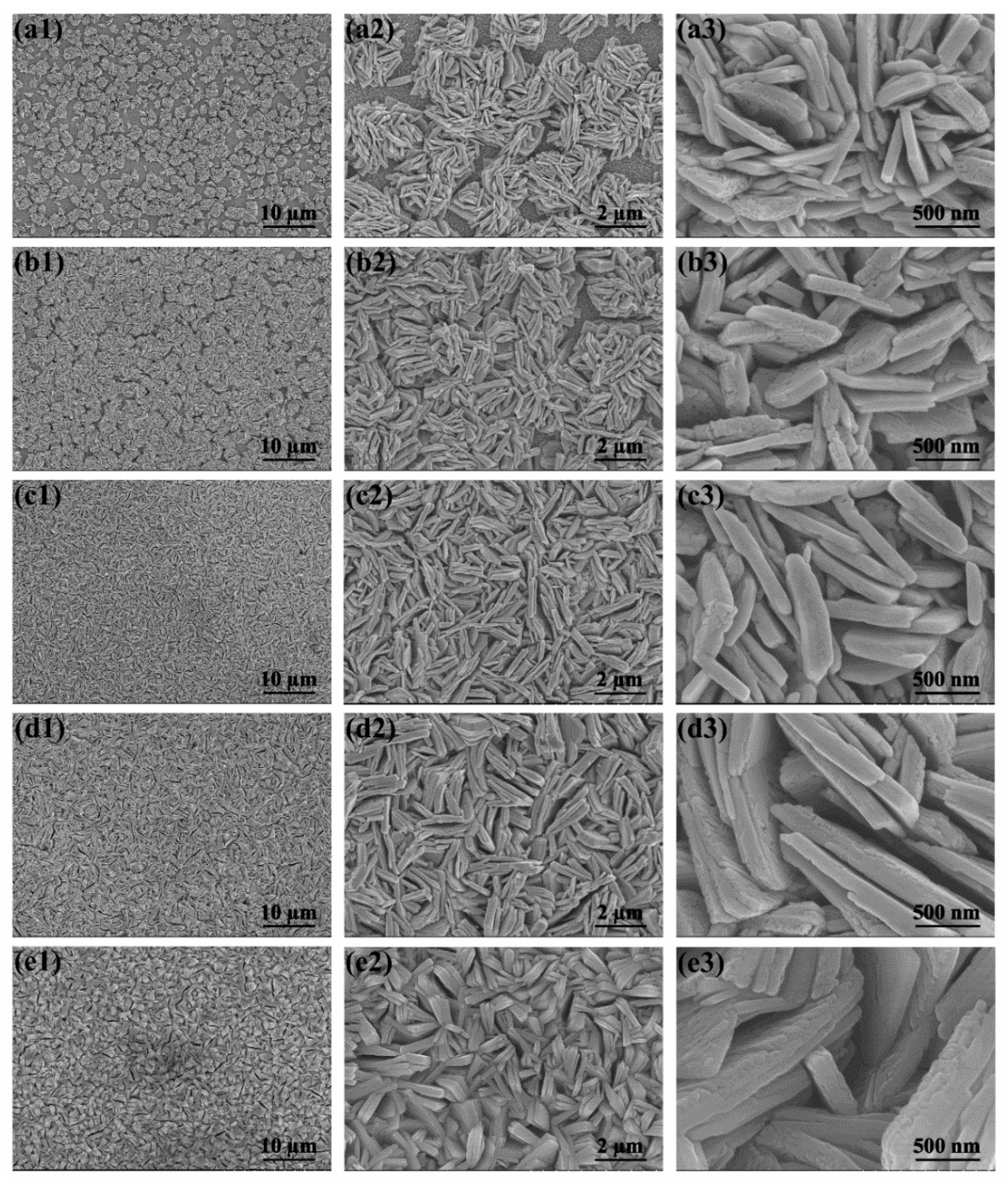
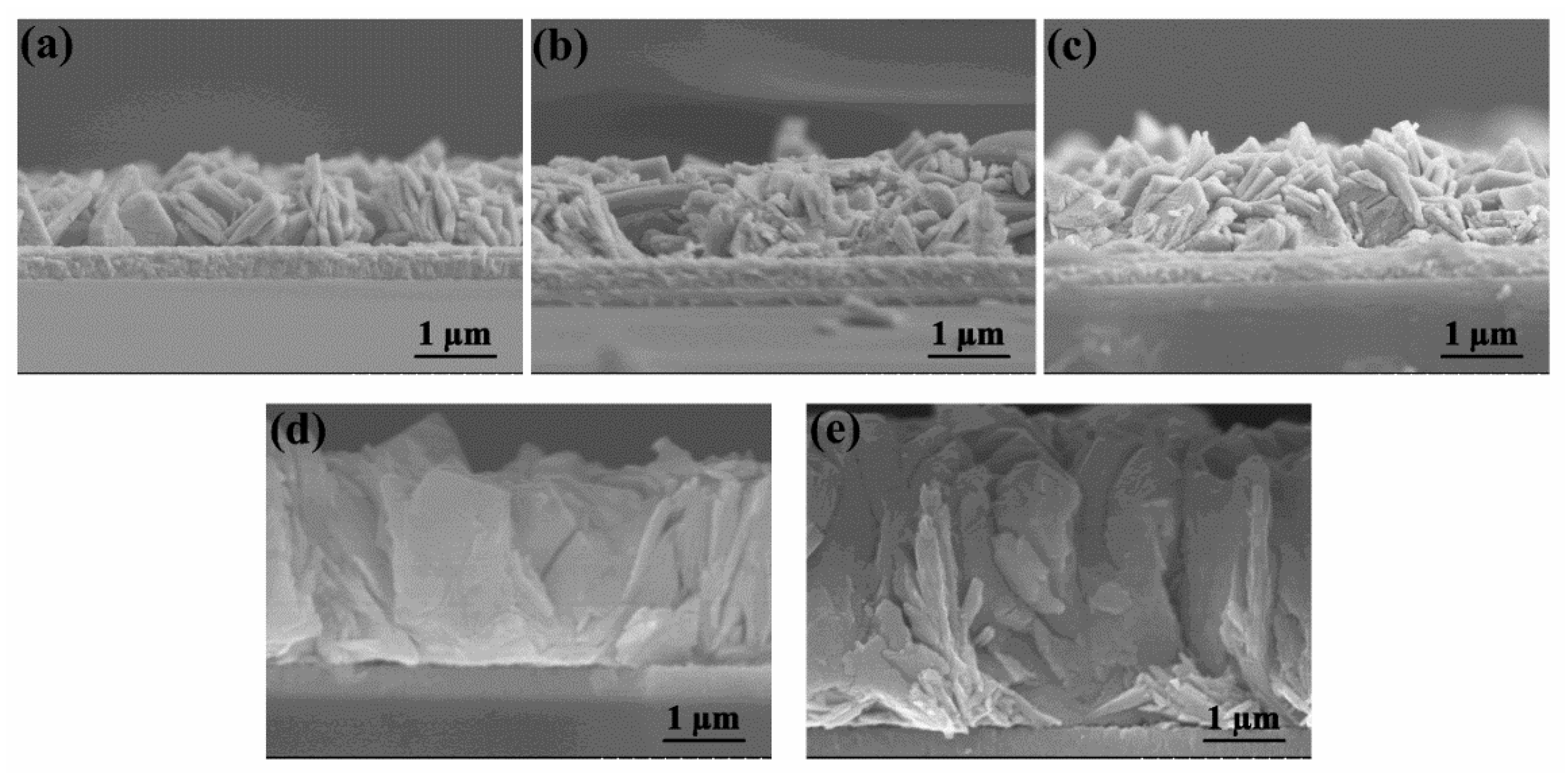
2.1. Structure and Properties of WO3 Nanoflake Arrays

Firstly, the WO3 morphology was optimized by changing the concentration of hydrothermal precursors. Figure 1 and Figure 2 exhibit SEM images of different WO3 films from the top and cross-sectional view, respectively. It can be seen that all of the WO3 films are featured with nanoflake structure, which are arranged directly onto the FTO substrate. When the concentration of sodium tungstate in precursor solution is low (10 mM), nanoflower clusters assembled by thin nanoflakes appear in WO3-a, which are uniformly distributed on FTO substrate with a relatively large exposed FTO space. As seen in Figure 2a, the thickness of the WO3-a array is about 1.2 μm. As for WO3-b, the distribution of the WO3 nanoflower structure gets distinctly denser with less exposed area of FTO (Figure 1(b1–b3)) and the thickness of the nanoflake array increases slightly to 1.3 μm (Figure 2b). When the concentration of sodium tungstate solution is increased to 20 mM, no nanoflowers appeared in WO3-c, where the morphology in a wide field of vision is the uniform nanoflake array. There is no FTO substrate exposed. As seen in Figure 2c, the thickness of WO3-c is about 1.5 μm. When the concentration of sodium tungstate solution is further increased to 50 or 80 mM, the WO3-c and WO3-d nanoflakes seen from the top view do not change much, with a slightly denser arrangement of the WO3 nanoflakes (Figure 1(d1–d3,e1–e3)). However, the thickness of the nanoflake arrays changes significantly.
As seen in Figure 2d, the thickness of WO3-d is about 3.2 μm, which is almost twice that of WO3-c. When the concentration of the sodium tungstate solution further increases to 80 mM, the thickness of the WO3-e array increases to 4.0 μm (Figure 2e). Combined with the images from Figure 1 and Figure 2, it can be concluded that the increase in precursor concentration in the initial stage mainly causes changes in the coverage of the film and the density of the nanoflakes, while the thickness of the WO3 array changes little. Whereas, when the nanoflakes completely cover the FTO substrate, further increase in precursor concentration mainly causes the increase in the thickness of the WO3 nanoflake array. Moreover, the morphology of nanoflake arrays directly grown on FTO substrates can not only provide a large specific surface area, but also facilitate the efficient transfer of photogenerated electrons to the FTO collector.
To confirm the phase composition of the WO3 arrays, Figure 3 gives the XRD patterns of WO3 arrays obtained through the hydrothermal process before and after heat treatment. Taking WO3-d in Figure 3a as an example, before heat treatment, strong diffraction peaks appear at 16.5°, 19.3°, 23.8°, 25.7°, 30.5°, 35.1°, 38.9°, 49.2° and 52.9°, which respectively can be corresponded to the crystal faces of (020), (011), (120), (111), (031), (002), (022), (042) and (222) from WO3·H2O (JCPDS No. 43-0679). The diffraction peaks marked by black dots are from the FTO substrate. The XRD patterns of WO3 arrays prepared after calcination are given in Figure 3b. There are no diffraction peaks corresponding to WO3·H2O, indicating that all of the WO3·H2O phase has inversed after heat treatment at 500 °C. Instead, all of the peaks are from monoclinic tungsten oxide (JCPDS 43-1035), where the respective peaks at 23.1°, 23.6°, 24.4°, 34.2° and 50.0° can, respectively, be ascribed to the (002), (020), (200), (202) and (140) crystal planes [44]. In addition, it can be seen that after the same synthesis process, the intensity of WO3 diffraction peak gradually increases with the increase in the precursor concentration. These results are consistent with the SEM images that as the concentration of sodium tungstate solution increases, WO3 nanoflakes gradually cover the FTO substrate and then increase in thickness.
The photoelectrochemical water splitting performance of different WO3 nanoarrays was studied by using them as the working electrodes and the results are shown in Figure 4. According to the linear sweep voltammograms curve (LSV) in Figure 4a, under illumination the onset potential of each WO3 array is similar, which is about 0.69 V (vs. RHE). For WO3-a, it has the lowest water splitting performance with a photocurrent at 1.23 V (vs. RHE) being 0.92 mA cm−2. According to the UV-Visible light absorption performance (Supplementary Figure S1), WO3-a has limited absorption of incident light. The insufficient photogenerated electrons and holes lead to the lowest photocurrent. With the increase in precursor concentration, the photocurrent gradually increases, where the photocurrent of WO3-b, WO3-c and WO3-d is 1.26, 1.50 and 1.69 mA cm−2, respectively. When the concentration of precursor solution is further increased, the photocurrent of WO3-e decreased to 1.63 mA cm−2. Combined with the SEM images, the WO3 nanoflake arrays initially get denser and thicker with the increase in the precursor solution concentration, which can increase the light absorption and photocarrier generation so as to improve the photocurrent of photoelectrochemical water oxidation. On the contrary, the thick film of WO3-e could extend the distance of photogenerated electrons to the FTO collector, which increases the probability of carrier recombination and is not conducive to the effective separation of carriers. Thus, the WO3-d shows the largest photocurrent as a result of a balance of photocarrier generation and separation. Figure 4b shows the curves of applied bias photon-to-current (ABPE) conversion efficiency at the applied bias of 0.98 V (vs. RHE). Among them, the ABPE of WO3-d reaches the maximum value at about 0.23%, indicating that it has a good photon-to-current conversion efficiency.

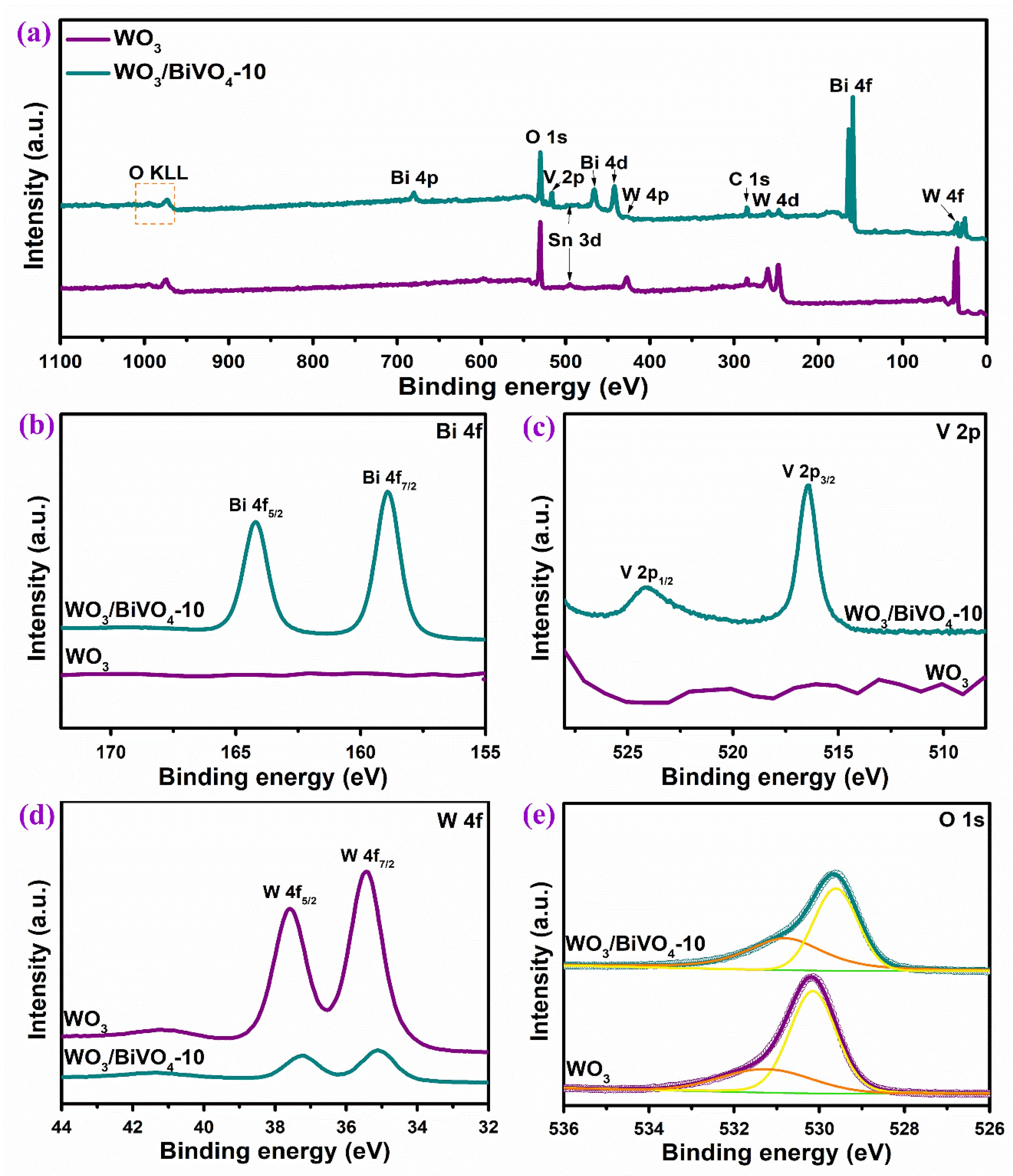
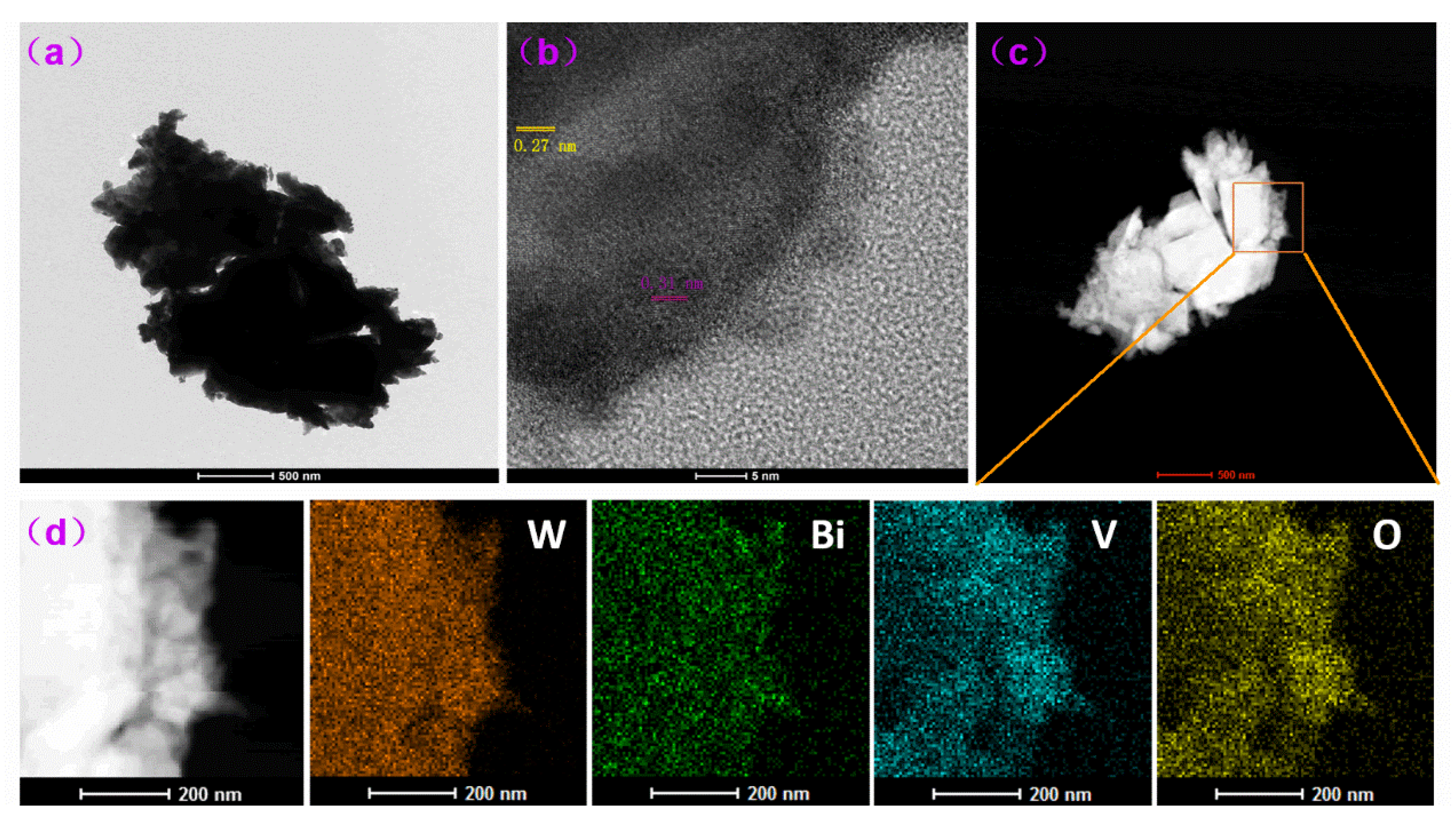
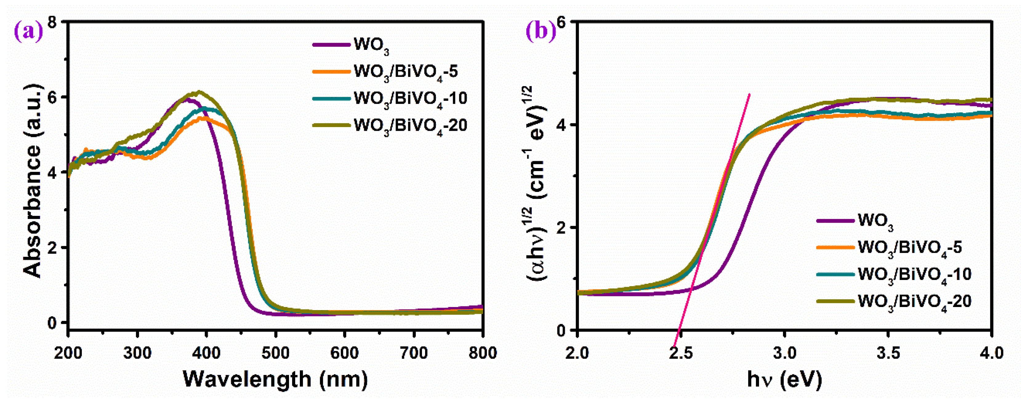
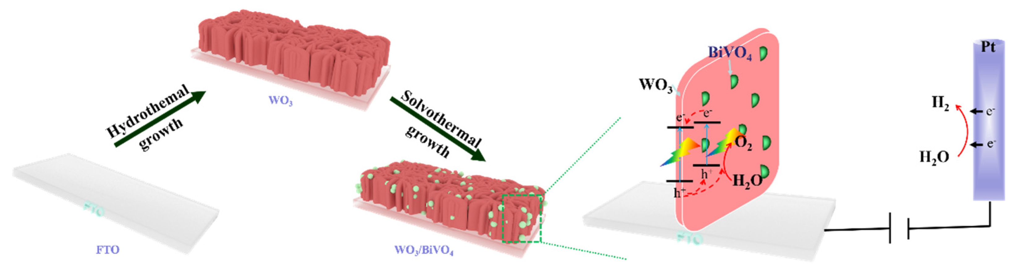
2.2. Structure and Properties of WO3/BiVO4 Nanoarrays

Based on the structure and properties of the WO3 arrays, WO3-d was chosen to composite BiVO4 for further research. Figure 5 gives the XRD patterns of the WO3/BiVO4 composite array prepared with different concentrations of BiVO4 precursors. In addition to the peaks of WO3 and FTO substrate (marked with black circles), new weak peaks appear, and the intensity of these peaks gradually increases with the increase in the concentration of BiVO4 precursor solution. Taking WO3 and WO3/BiVO4-10 as an example, it can be seen from the magnified XRD in Figure 5b that new diffraction peaks at 18.7°, 28.6°, 28.8°, 28.9° and 30.5° in WO3/BiVO4-10 can, respectively, be corresponded to the (110), (−130), (−121), (121) and (040) crystal faces of monoclinic scheelite BiVO4 (JCPDS No. 14-0688) [45]. Therefore, the existence of BiVO4 is proved, and the relatively weak diffraction peaks of BiVO4 might be ascribed to the low content of BiVO4. The small peak around 27.8° can be assigned to the (011) crystal face of the tiny VO2 (JCPDS No. 43-1051) after the hydrothermal route.
The morphology of the WO3/BiVO4 composite prepared with different concentrations of BiVO4 precursor solution were observed by SEM. As shown in Figure 6, the nanoflake structure of the WO3 array was still maintained after solvothermal reaction. From the morphology of WO3/BiVO4-5 in Figure 6b, small nanoparticles can be clearly verified on the WO3 nanoflake with a particle size of ~20 nm, which are uniformly attached to the WO3 nanoflakes. As the reaction concentration of precursors increases, the distributed BiVO4 on the surface of the WO3 nanoflake becomes denser. For WO3/BiVO4-10, it can be seen from Figure 6c that the size of BiVO4 nanoparticles increases to ~50 nm and there is a uniform dispersion of BiVO4 nanoparticles on the surface of the entire WO3 nanoflake array. When the reaction concentration further rises to 20 mM, as shown in Figure 6d, WO3/BiVO4-20 is covered with not only uniform BiVO4 nanoparticles but also aggregated nanoparticles. As shown in Supplementary Figure S2, the size of large BiVO4 particles in WO3/BiVO4-20 can be as large as ~1 μm. Therefore, by controlling the proper precursor concentration, the surface dispersed morphology of BiVO4 nanoparticles on the surface of WO3 nanoflakes is fabricated, which is conducive to expanding the interfacial surface area and increasing the reactive sites.
The cross-sectional SEM image of WO3/BiVO4-10 is illustrated in Supplementary Figure S3. The thickness of WO3/BiVO4-10 is similar to that of the pure WO3 arrays, which means the solvothermal progress does not change the morphology of WO3 arrays. BiVO4 nanoparticles can also be verified from the cross-sectional view, further indicating the formation of the surface dispersed morphology of BiVO4-nanoparticle@WO3-nanoflake. Sn distribution is consistent with the position of FTO substrate. From the element mapping, Bi, V, W and O elements are distributed uniformly, indicating that BiVO4 particles are uniformly loaded on the entire longitudinal WO3 nanoflakes.
Representative XPS spectra were tested to study the chemical elemental composition and the corresponding elemental valence states of the WO3 and WO3/BiVO4 arrays. The survey spectrum in Figure 7a proves that WO3 contains W and O elements, while WO3/BiVO4-10 contains Bi, V, W and O elements. From the high-resolution spectra of Bi 4f and V 2p in Figure 7b,c, the WO3 array shows basically a straight line. After BiVO4 loaded, WO3/BiVO4-10 showed two peaks at 164.2 and 158.9 eV, ascribed to the binding energy of Bi 4f5/2 and Bi 4f7/2, respectively. This indicates that the Bi element is presented in the form of Bi3+ [46]. The binding energies at 524.1 and 516.5 eV indicate the existence of V 2p1/2 and V 2p3/2 [47]. According to the high-resolution XPS spectra of W 4f in Figure 7d, the binding energies of W 4f5/2 and W 4f7/2 in the WO3 nanoarrays are located at 35.4 and 37.6 eV, which proves the chemical state of W element in the form of W6+ [44]. For the WO3/BiVO4 composite array, the intensity of W 4f spectrum is obviously weakened after the deposition of BiVO4 on WO3. In addition, the binding energy of W 4f moves towards the lower energy direction, which proves that there is a strong interaction between WO3 and BiVO4, which is beneficial for electron conduction. The high-resolution XPS spectra of O 1s shown in Figure 7e can be fitted into two peaks located at 530.1 and 531.4 eV, corresponding to lattice oxygen and defect sites with low oxygen coordination (i.e., hydroxyl), respectively.
The WO3/BiVO4-10 composite array was scraped off the substrate for TEM test. A representative image is shown in Figure 8a and its corresponding HRTEM image is shown in Figure 8b, where the lattice spacing from the nanoflake structure is around 0.27 nm, ascribed to the (022) interplanar spacing of monoclinic WO3. The lattice spacing of surface loaded particles is ~0.31 nm, which is consistent with the (−121) crystal plane of BiVO4. In addition, the tight lattice connection between BiVO4 and WO3 further indicates a good binding between BiVO4 and WO3. From Figure 8c, the nanoflake structure of WO3 can be distinguished. As shown in the element distribution images (Figure 8d), W element can be seen in the whole field of vision, while Bi and V elements are relatively distributed in the marginal region corresponding to small particles. The distribution of Bi, V, W and O elements indicates that BiVO4 is evenly distributed on the surface of WO3.
Figure 9 is the optical absorption performance of WO3 and WO3/BiVO4 arrays. Pure WO3 exhibits a light response to ultraviolet light and part of visible light. After loading BiVO4, the light response range of the WO3/BiVO4 array shows an obvious red shift, but the light absorption intensity is similar in the ultraviolet region. The results show that the absorbed light of 400–480 nm is mainly due to the contribution of BiVO4, and the utilization of visible light by WO3/BiVO4 is significantly improved after loading BiVO4. The corresponding Tauc curve is given in Figure 9b, where the band gap can be estimated by extending the linear part of the curve. The band gap of the WO3/BiVO4 composite array is about 2.50 eV, which is significantly reduced compared with that of the pure WO3 array (2.64 eV), indicating a wider light spectrum of the WO3/BiVO4 composite.
The performance of WO3 and WO3/BiVO4 toward photoelectrochemical water oxidation was measured by using the WO3 and WO3/BiVO4 arrays as photoanodes. As shown in the linear sweep voltammograms curves (Figure 10a), the properties of WO3/BiVO4 are significantly improved compared with pure WO3. The dashed line represents the LSV curve of WO3/BiVO4 in the dark, which indicates the significant photoresponse of all photoanodes. As mentioned above, the photocurrent at 1.23 V (vs. RHE) of pure WO3 is 1.69 mA cm−2. After loading BiVO4, the photocurrent of WO3/BiVO4-5 was significantly increased to 2.57 mA cm−2. According to the above analysis, the absorption of visible light in the WO3/BiVO4 composite array is significantly increased, and the formation of the heterojunction structure between WO3 and BiVO4 is conducive to the effective separation of photogenerated carriers. As for the WO3/BiVO4-10 photoanode, the highest photocurrent at 3.53 mA cm−2 is observed. This performance may be due to the appropriate loading amount and excellent dispersion of BiVO4 in WO3/BiVO4-10, which enables the sufficient light absorption and effective carrier separation at the same time. As a result, more carriers can effectively transfer to the electrode surface for PEC OER reactions to take place. The key characteristics of recent reported WO3/BiVO4 heterojunction photoanodes without an additional catalyst or doping for solar water oxidation are summarized in Table 1. Considering that the photocurrent can be significantly improved if there is the hole scavenge in the electrolyte, the performance of the surface dispersed WO3/BiVO4 nanoplates in our work are among the best. In the case of WO3/BiVO4-20, the photocurrent then decreases to 2.95 mA cm−2. It has been reported that the short life of photogenerated electrons is the main drawback of the PEC performance of BiVO4. The agglomeration and the existence of large size BiVO4 in WO3/BiVO4-20 might hinder the effective carrier transfer, resulting in the decreased photocurrent in spite of the increased BiVO4 loading. Figure 10b shows the i–t curves of WO3 and the WO3/BiVO4 arrays measured with chopped light illumination. All the photoelectrodes exhibit prompt response toward light, indicating that the photoanode material has excellent transfer ability of photogenerated electrons and holes. The photocurrents of WO3, WO3/BiVO4-5, WO3/BiVO4-10 and WO3/BiVO4-20 photoanodes are 1.69, 2.84, 3.92 and 2.30 mA cm−2, which is consistent with the trend of LSV results.
The electrochemical impedance spectra of WO3 and WO3/BiVO4 arrays are shown in Figure 10c to characterize the impedance at the semiconductor/electrolyte interface. The corresponding equivalent circuit is provided in Supplementary Figure S4. RS stands for the series resistance. CPE is constant phase element and Rct represents the charge transfer resistance of the electrode/electrolyte interface. The radius of the arc in the impedance spectrum indicates the charge transfer ability of the photoanodes, where the smaller the radius means the smaller the impedance and a better charge transfer ability. Compared with pure WO3, the charge transfer impedance of WO3/BiVO4 decreases significantly, indicating that compositing BiVO4 can effectively reduce the charge transfer impedance of the photoelectrode due to the formation of the heterojunction. Among the WO3/BiVO4 composite arrays, WO3/BiVO4-10 has the lowest charge transfer impedance, which is the most favorable for photogenerated carriers to transfer to the electrode surface to oxidize water. The arc radius of WO3/BiVO4-20 is larger than that of WO3/BiVO4-10, which further indicates that the larger charge transfer impedance of WO3/BiVO4-20 limits its PEC water oxidation performance. This is consistent with the morphology analysis results. Figure 10d is the photocurrent stability test of WO3 and WO3/BiVO4-10 measured at 1.23 V (vs. RHE). Since WO3 is easily oxidized, the stability is poor. After loading BiVO4, the stability of WO3/BiVO4-10 was significantly improved; there was no significant drop during subsequent tests except for the initial current drop. The protective effect of the BiVO4 layer for WO3 can be verified. The formation of the WO3/BiVO4 heterojunction contributes to the enhanced separation of charge carriers and relieves the charge accumulation on the WO3 surface.
The fabrication and the PEC water oxidation mechanism of the surface dispersed WO3/BiVO4 heterojunction is schematically illustrated in Figure 11. The BiVO4-nanoparticle@ WO3-nanoflake structure, verified by the SEM and TEM measurements, can be prepared by carefully controlling the hydrothermal and solvothermal conditions. When used as photoanodes, both WO3 and BiVO4 can absorb light and generate an enhanced charge carrier. Subsequently, the WO3/BiVO4 heterojunction promotes the directional migration of photogenerated carriers and, thus, improves charge separation across the WO3 and BiVO4 interface, where the WO3 layer with better charge transfer ability has proper thickness to work as a skeleton to optimize the light absorption and provide the electron pathway to the FTO substrate at the same time. Meanwhile, the BiVO4 nanoparticles with little size promote light absorption and facilitate charge carrier transfer. In addition, the surface dispersed structure of the BiVO4-nanoparticle@ WO3-nanoflake ensures that the photogenerated holes from both WO3 and BiVO4 can contribute to PEC water oxidation, which greatly helps to suppress the accumulation and recombination of charge carriers at the semiconductor interface, as confirmed by the increased photocurrent as well as stability.

3. Materials and Methods

3.1. Preparation of the WO3 Nanoflake Arrays

All chemical reagents used in this work are analytical reagent. The tungsten trioxide nanoflake arrays were grown directly on the surface of F doped tin oxide (FTO) glass by the hydrothermal method, with sodium tungstate as tungsten source and oxalic acid as morphology control agent. Specifically, a certain amount of sodium tungstate and oxalic acid was weighed and dissolved completely in deionized water, where the molar ratio of Na2WO4 and H2C2O4 was controlled at 1:2. Then, 0.5 mL of concentrated HCl was dropwise added into the above mixed solution. A piece of FTO conductive glass was placed in a reaction kettle and a certain amount of the above precursor solution was added. After the hydrothermal treatment at 150 °C for 4 h, we can observe a yellow film on the surface of the FTO. Finally, the WO3 nanoflake arrays were obtained by heat treatment at 500 °C for 2 h in air. In order to optimize the synthesis conditions of the WO3 film, precursors with different concentrations of sodium tungstate of 10, 15, 20, 50 and 80 mM were prepared and the corresponding WO3 films were denoted as WO3-a, WO3-b, WO3-c, WO3-d and WO3-e.

3.2. Preparation of the WO3/BiVO4 Nanoflake Arrays

The WO3/BiVO4 composite films were further prepared by the solvothermal method. A certain amount of Bi(NO3)3·5H2O was weighed and dissolved in ethylene glycol to obtain a colorless transparent solution. Afterwards, the equal molar mass NH4VO3 was added and stirred at an accelerated speed for another 20 min to form a uniform yellow suspension. The above-obtained WO3 film on FTO was placed in a reaction kettle. After the solvothermal reaction at 160 °C for 4 h, the film was fully rinsed with distilled water, dried in the oven at 60 °C and changed into the WO3/BiVO4 composite film by heat treatment at 500 °C in air. By controlling the concentration of Bi(NO3)3·5H2O and NH4VO3 solution at 5, 10 and 20 mM, the WO3/BiVO4 films with different amounts of BiVO4 were prepared, which were abbreviated as WO3/BiVO4-5, WO3/BiVO4-10 and WO3/BiVO4-20, respectively.

3.3. Characterization

The X-ray diffraction (XRD) data of all samples were collected on Bruker’s D8 advance diffractometer (Karlsruhe, Germany). The surface chemical composition of sample was analyzed by the X-ray photoelectron spectra (XPS) on an ESCALab220i-XL electron spectrometer (Thermo Scientific, Waltham, MA, USA). The Hitachi S4800 (Tokyo, Japan) was used to obtain the scanning electron microscope (SEM) images. The transmission electron microscopy (TEM) images and the elemental mapping images were measured on Philips Tecnai G2 (Thermo Fisher, Waltham, MA, USA). UV-vis diffuse reflectance spectra were reflected by the UV-3600 spectrophotometer (Shimadzu, Tokyo, Japan).

3.4. Photoelectrochemical Tests

The photoelectrochemical tests of the photoanodes were measured by the three-electrode system on photoelectrochemical workstation (Zahner IM6, Zahner, Kronach, Germany), where the photoanode was used as the working electrode, Pt electrode as the counter electrode and saturated calomel electrode as the reference electrode. The simulated standard sunlight was the light source. The 0.2 mol L−1 potassium phosphate buffer solution (pH = ~7) was used as electrolyte. PEC water oxidation was evaluated by the linear sweep voltammograms (LSV). The electrochemical impedance spectra (EIS) were measured from a frequency of 100,000 Hz to 0.1 Hz with a disturbing current voltage of 10 mV.

4. Conclusions

The WO3/BiVO4 composite photoanode with a structure of surface dispersed heterojunction was constructed, where a monoclinic WO3 nanoflake array was grown on FTO substrate, with optimized morphology and thickness by controlling the appropriate concentration of precursor solution. The BiVO4 nanoparticles were then uniformly loaded on the WO3 nanoflakes using the solvothermal method. When used as photoanode, the WO3/BiVO4 composite exhibits superior PEC water oxidation performance with photocurrent of 3.53 mA cm−2, which is twice that of pure WO3 photoanode. This improved performance comes from the advantages of the unique surface dispersed WO3/BiVO4 array structure, as follows: (1) the proper thickness of the WO3/BiVO4 composites balanced the light absorption and the charge separation, contributing to more charge carriers reaching the interface; (2) the formation of the heterojunction immensely improves the separation efficiency of interfacial charge carriers; and (3) the surface dispersed heterojunction structure of BiVO4-nanoparticle@WO3-nanoflake provides a large heterojunction interface, which offers a large surface area and improves the stability of the photoelectrode.

Supplementary Materials

The following supporting information can be downloaded at: https://www.mdpi.com/article/10.3390/molecules29020372/s1, Figure S1: (a) UV-vis absorption spectra and (b) Tauc plots of WO3 arrays; Figure S2: SEM images of WO3/BiVO4 composite arrays, (a) WO3/BiVO4-5, (b) WO3/BiVO4-10, (c) WO3/BiVO4-20; Figure S3: Cross-sectional view SEM image of WO3/BiVO4-10 and the corresponding elemental mapping; Figure S4: The equivalent circuit of the electrochemical impedance spectra.

Author Contributions

Conceptualization, T.W. and J.H.; methodology, X.F.; validation, B.G. and L.S.; formal analysis, B.G.; writing—original draft preparation, X.F. and Q.C.; writing—review and editing, X.F., Q.C., F.Z. and T.W.; supervision, J.H.; project administration, X.F.; funding acquisition, X.F. All authors have read and agreed to the published version of the manuscript.

Funding

The authors express their great appreciation of the financial support from the Scientific Research Foundation of Nanjing Institute of Technology (YKJ202007), and the Natural Science Foundation of Jiangsu Province (BK20190413 and BK20210616), the China Postdoctoral Science Foundation (2019M661825), Jiangsu Key Laboratory of Electrochemical Energy-Storage Technologies (EEST2021-2).

Institutional Review Board Statement

Not applicable.

Informed Consent Statement

Not applicable.

Data Availability Statement

Data are contained within the article and Supplementary Materials.

Conflicts of Interest

The authors declare no conflicts of interest.

References

  1. Samuel, E.; Joshi, B.; Kim, M.W.; Swihart, M.T.; Yoon, S.S. Morphology engineering of photoelectrodes for efficient photoelectrochemical water splitting. Nano Energy 2020, 72, 104648. [Google Scholar] [CrossRef]
  2. Mushtaq, M.A.; Kumar, A.; Yasin, G.; Arif, M.; Tabish, M.; Ibraheem, S.; Cai, X.; Ye, W.; Fang, X.; Saad, A.; et al. 3D interconnected porous Mo-doped WO3@CdS hierarchical hollow heterostructures for efficient photoelectrochemical nitrogen reduction to ammonia. Appl. Catal. B Environ. 2022, 317, 121711. [Google Scholar] [CrossRef]
  3. Daulbayev, C.; Sultanov, F.; Bakbolat, B.; Daulbayev, O. 0D, 1D and 2D nanomaterials for visible photoelectrochemical water splitting. A Review. Int. J. Hydrogen Energy 2020, 45, 33325–33342. [Google Scholar] [CrossRef]
  4. Marwat, M.A.; Humayun, M.; Afridi, M.W.; Zhang, H.; Karim, M.R.A.; Ashtar, M.; Usman, M.; Waqar, S.; Ullah, H.; Wang, C.; et al. Advanced catalysts for photoelectrochemical water splitting. ACS Appl. Energy Mater. 2021, 4, 12007–12031. [Google Scholar] [CrossRef]
  5. Tang, J.; Durrant, J.R.; Klug, D.R. Mechanism of photocatalytic water splitting in TiO2. Reaction of water with photoholes, importance of charge carrier dynamics, and evidence for four-hole chemistry. J. Am. Chem. Soc. 2008, 130, 13885–13891. [Google Scholar] [CrossRef] [PubMed]
  6. Yao, B.; Zhang, J.; Fan, X.; He, J.; Li, Y. Surface engineering of nanomaterials for photo-electrochemical water splitting. Small 2019, 15, 1803746. [Google Scholar] [CrossRef]
  7. Zhang, X.; Wang, X.; Wang, D.; Ye, J. Conformal BiVO4-layer/WO3-nanoplate-array heterojunction photoanode modified with cobalt phosphate cocatalyst for significantly enhanced photoelectrochemical performances. ACS Appl. Mater. Interfaces 2019, 11, 5623–5631. [Google Scholar] [CrossRef]
  8. Li, H.; Lin, C.; Yang, Y.; Dong, C.; Min, Y.; Shi, X.; Wang, L.; Lu, S.; Zhang, K. Boosting Reactive Oxygen Species Generation Using Inter-Facet Edge Rich WO3 Arrays for Photoelectrochemical Conversion. Angew. Chem. Int. Ed. 2023, 62, e202210804. [Google Scholar] [CrossRef]
  9. Han, H.; Riboni, F.; Karlický, F.; Kment, S.; Goswami, A.; Sudhagar, P.; Yoo, J.; Wang, L.; Tomanec, O.; Petr, M.; et al. α-Fe2O3/TiO2 3D hierarchical nanostructures for enhanced photoelectrochemical water splitting. Nanoscale 2017, 9, 134–142. [Google Scholar] [CrossRef]
  10. Wang, L.; Si, W.; Ye, Y.; Wang, S.; Hou, F.; Hou, X.; Cai, H.; Dou, S.X.; Liang, J. Cu-ion-implanted and polymeric carbon nitride-decorated TiO2 nanotube array for unassisted photoelectrochemical water splitting. ACS Appl. Mater. Interfaces 2021, 13, 44184–44194. [Google Scholar] [CrossRef]
  11. Chaulagain, N.; Alam, K.M.; Kadian, S.; Kumar, N.; Garcia, J.; Manik, G.; Shankar, K. Synergistic enhancement of the photoelectrochemical performance of TiO2 nanorod arrays through embedded plasmon and surface carbon nitride co-sensitization. ACS Appl. Mater. Interfaces 2022, 14, 24309–24320. [Google Scholar] [CrossRef]
  12. Han, J.; Liu, Z. Optimization and modulation strategies of zinc oxide-based photoanodes for highly efficient photoelectrochemical water splitting. ACS Appl. Energy Mater. 2021, 4, 1004–1013. [Google Scholar] [CrossRef]
  13. Xie, X.; Wang, R.; Ma, Y.; Chen, J.; Cui, Q.; Shi, Z.; Li, Z.; Xu, C. Photothermal-effect-enhanced photoelectrochemical water splitting in MXene-nanosheet-modified ZnO nanorod arrays. ACS Appl. Nano Mater. 2022, 5, 11150–11159. [Google Scholar] [CrossRef]
  14. Zhang, Y.; Zhang, H.; Ji, H.; Ma, W.; Chen, C.; Zhao, J. Pivotal role and regulation of proton transfer in water oxidation on hematite photoanodes. J. Am. Chem. Soc. 2016, 138, 2705–2711. [Google Scholar] [CrossRef] [PubMed]
  15. Wang, P.; Wang, S.; Gao, L.; Long, X.; Chai, H.; Li, F.; Wang, Q.; Jin, J. Achieving surface-sealing of hematite nanoarray photoanode with controllable metal–organic frameworks shell for enhanced photoelectrochemical water oxidation. J. Catal. 2022, 413, 398–406. [Google Scholar] [CrossRef]
  16. Yuan, S.Y.; Jiang, L.W.; Hu, J.S.; Liu, H.; Wang, J.J. Fully dispersed irox atomic clusters enable record photoelectrochemical water oxidation of hematite in acidic media. Nano Lett. 2023, 23, 2354–2361. [Google Scholar] [CrossRef]
  17. Kong, W.; Zhang, X.; Liu, S.; Zhou, Y.; Chang, B.; Zhang, S.; Fan, H.; Yang, B. N doped carbon dot modified WO3 nanoflakes for efficient photoelectrochemical water oxidation. Adv. Mater. Interfaces 2019, 6, 1801653. [Google Scholar] [CrossRef]
  18. Wu, H.; Liu, Q.; Zhang, L.; Tang, Y.W.; Wang, G.; Mao, G.B. Novel nanostructured WO3@prussian blue heterojunction photoanodes for efficient photoelectrochemical water splitting. ACS Appl. Energy Mater. 2021, 4, 12508–12514. [Google Scholar] [CrossRef]
  19. Bu, Y.; Ren, J.; Zhang, H.; Yang, D.; Chen, Z.; Ao, J.P. Photogenerated-carrier separation along edge dislocation of WO3 single-crystal nanoflower photoanode. J. Mater. Chem. A 2018, 6, 8604–8611. [Google Scholar] [CrossRef]
  20. Kim, J.H.; Lee, J.S. Elaborately modified BiVO4 photoanodes for solar water splitting. Adv. Mater. 2019, 31, 1806938. [Google Scholar] [CrossRef]
  21. Lin, J.; Han, X.; Liu, S.; Lv, Y.; Li, X.; Zhao, Y.; Li, Y.; Wang, L.; Zhu, S. Nitrogen-doped cobalt-iron oxide cocatalyst boosting photoelectrochemical water splitting of BiVO4 photoanodes. Appl. Catal. B Environ. 2023, 320, 121947. [Google Scholar] [CrossRef]
  22. Jiang, W.; An, Y.; Wang, Z.; Wang, M.; Bao, X.; Zheng, L.; Cheng, H.; Wang, P.; Liu, Y.; Zheng, Z.; et al. Stress-induced BiVO4 photoanode for enhanced photoelectrochemical performance. Appl. Catal. B Environ. 2022, 304, 121012. [Google Scholar] [CrossRef]
  23. Grigioni, I.; Stamplecoskie, K.G.; Selli, E.; Kamat, P.V. Dynamics of photogenerated charge carriers in WO3/BiVO4 heterojunction photoanodes. J. Phys. Chem. C 2015, 119, 20792–20800. [Google Scholar] [CrossRef]
  24. Afroz, K.; Moniruddin, M.; Bakranov, N.; Kudaibergenov, S.; Nuraje, N. A heterojunction strategy to improve the visible light sensitive water splitting performance of photocatalytic materials. J. Mater. Chem. A 2018, 6, 21696–21718. [Google Scholar] [CrossRef]
  25. Tateno, H.; Chen, S.Y.; Miseki, Y.; Nakajima, T.; Mochizuki, T.; Sayama, K. Photoelectrochemical oxidation of glycerol to dihydroxyacetone over an acid-resistant Ta: BiVO4 photoanode. ACS Sustain. Chem. Eng. 2022, 10, 7586–7594. [Google Scholar] [CrossRef]
  26. Kim, J.-H.; Kim, D.H.; Yoon, J.W.; Dai, Z.; Lee, J.-H. Rational design of branched WO3 nanorods decorated with BiVO4 nanoparticles by all-solution processing for efficient photoelectrochemical water splitting. ACS Appl. Energy Mater. 2019, 2, 4535–4543. [Google Scholar] [CrossRef]
  27. Hong, S.J.; Lee, S.; Jang, J.S.; Lee, J.S. Heterojunction BiVO4/WO3 electrodes for enhanced photoactivity of water oxidation. Energy Environ. Sci. 2011, 4, 1781–1787. [Google Scholar] [CrossRef]
  28. Rao, P.M.; Cai, L.; Liu, C.; Cho, I.S.; Lee, C.H.; Weisse, J.M.; Yang, P.; Zheng, X. Simultaneously efficient light absorption and charge separation in WO3/BiVO4 core/shell nanowire photoanode for photoelectrochemical water oxidation. Nano Lett. 2014, 14, 1099–1105. [Google Scholar] [CrossRef]
  29. Shi, X.; Choi, Y.; Zhang, K.; Kwon, J.; Kim, D.Y.; Lee, J.K.; Oh, S.H.; Kim, J.K.; Park, J.H. Efficient photoelectrochemical hydrogen production from bismuth vanadate-decorated tungsten trioxide helix nanostructures. Nat. Commun. 2014, 5, 4775. [Google Scholar] [CrossRef]
  30. Ma, Z.; Song, K.; Wang, L.; Gao, F.; Tang, B.; Hou, H.; Yang, W. WO3/BiVO4 type-II heterojunction arrays decorated with oxygen-deficient ZnO passivation layer: A highly efficient and stable photoanode. ACS Appl. Mater. Interfaces 2019, 11, 889–897. [Google Scholar] [CrossRef]
  31. Ma, M.; Kim, J.K.; Zhang, K.; Shi, X.; Kim, S.J.; Moon, J.H.; Park, J.H. Double-deck inverse opal photoanodes: Efficient light Absorption and charge separation in heterojunction. Chem. Mater. 2014, 26, 5592–5597. [Google Scholar] [CrossRef]
  32. Ma, M.; Shi, X.; Zhang, K.; Kwon, S.; Li, P.; Kim, J.K.; Phu, T.T.; Yi, G.-R.; Park, J.H. A 3D triple-deck photoanode with a strengthened structure integrality: Enhanced photoelectrochemical water oxidation. Nanoscale 2016, 8, 3474–3481. [Google Scholar] [CrossRef] [PubMed]
  33. Zeng, Q.; Li, J.; Li, L.; Bai, J.; Xia, L.; Zhou, B. Synthesis of WO3/BiVO4 photoanode using a reaction of bismuth nitrate with peroxovanadate on WO3 film for efficient photoelectrocatalytic water splitting and organic pollutant degradation. Appl. Catal. B Environ. 2017, 217, 21–29. [Google Scholar] [CrossRef]
  34. Park, E.; Patil, S.S.; Lee, H.; Kumbhar, V.S.; Lee, K. Photoelectrochemical H2 evolution on WO3/BiVO4 enabled by single-crystalline TiO2 overlayer modulations. Nanoscale 2021, 13, 16932–16941. [Google Scholar] [CrossRef] [PubMed]
  35. Patil, S.S.; Lee, J.; Park, E.; Nagappagari, L.R.; Lee, K. Interstitial M+ (M+ = Li+ or Sn4+) doping at interfacial BiVO4/WO3 to promote photoelectrochemical hydrogen production. ACS Appl. Energy Mater. 2021, 4, 13636–13645. [Google Scholar] [CrossRef]
  36. Grigioni, I.; Liberto, G.D.; Dozzi, M.V.; Tosoni, S.; Pacchioni, G.; Selli, E. WO3/BiVO4 photoanodes: Facets matching at the heterojunction and BiVO4 layer thickness effects. ACS Appl. Energy Mater. 2021, 4, 8421–8431. [Google Scholar] [CrossRef]
  37. Quang, N.D.; Van, P.C.; Majumder, S.; Jeong, J.-R.; Kim, D.; Kim, C. Optimization of photogenerated charge transport using type-II heterojunction structure of CoP/BiVO4:WO3 for high efficient solar-driver water splitting. J. Alloys Compd. 2022, 899, 163292. [Google Scholar] [CrossRef]
  38. Li, Y.; Mei, Q.; Liu, Z.; Hu, X.; Zhou, Z.; Huang, J.; Bai, B.; Liu, H.; Ding, F.; Wang, Q. Fluorine-doped iron oxyhydroxide cocatalyst: Promotion on the WO3 photoanode conducted photoelectrochemical water splitting. Appl. Catal. B Environ. 2022, 304, 120995. [Google Scholar] [CrossRef]
  39. Kalanur, S.S.; Yoo, I.-H.; Park, J.; Seo, H. Insights into the electronic bands of WO3/BiVO4/TiO2, revealing high solar water splitting efficiency. J. Mater. Chem. A 2017, 5, 1455–1461. [Google Scholar] [CrossRef]
  40. Lee, M.G.; Kim, D.H.; Sohn, W.; Moon, C.W.; Park, H.; Lee, S.; Jang, H.W. Conformally coated BiVO4 nanodots on porosity-controlled WO3 nanorods as highly efficient type II heterojunction photoanodes for water oxidation. Nano Energy 2016, 28, 250–260. [Google Scholar] [CrossRef]
  41. Kumbhar, V.S.; Lee, H.; Lee, J.; Lee, K. Interfacial growth of the optimal BiVO4 nanoparticles onto self-assembled WO3 nanoplates for efficient photoelectrochemical water splitting. J. Colloid Interface Sci. 2019, 557, 478–487. [Google Scholar] [CrossRef] [PubMed]
  42. Chi, Z.; Zhao, J.; Zhang, Y.; Yu, H.; Yu, H. Coral-like WO3/BiVO4 photoanode constructed via morphology and facet engineering for antibiotic wastewater detoxifcation and hydrogen recovery. Chem. Eng. J. 2022, 428, 131817. [Google Scholar] [CrossRef]
  43. Guo, H.; Zhang, Y.; Wang, S.; Li, L.; Wang, W.; Sun, Q. In-situ generation of Bi2S3 to construct WO3/BiVO4/Bi2S3 heterojunction for photocathodic protection of 304SS. J. Electroanal. Chem. 2022, 907, 116033. [Google Scholar] [CrossRef]
  44. Li, L.; Xiao, S.; Li, R.; Cao, Y.; Chen, Y.; Li, Z.; Li, G.; Li, H. Nanotube array-like WO3 photoanode with dual-layer oxygen evolution cocatalysts for photoelectrocatalytic overall water splitting. ACS Appl. Energy Mater. 2018, 1, 6871–6880. [Google Scholar] [CrossRef]
  45. Baek, J.H.; Kim, B.J.; Han, G.S.; Hwang, S.W.; Kim, D.R.; Cho, I.S.; Jung, H.S. BiVO4/WO3/SnO2 double-heterojunction photoanode with enhanced charge separation and visible-transparency for bias-free solar water-splitting with a perovskite solar cell. ACS Appl. Mater. Interfaces 2017, 9, 1479–1487. [Google Scholar] [CrossRef]
  46. Gao, Y.; Li, Y.; Yang, G.; Li, S.; Xiao, N.; Xu, B.; Liu, S.; Qiu, P.; Hao, S.; Ge, L. Fe2TiO5 as an efficient co-catalyst to improve the photoelectrochemical water splitting performance of BiVO4. ACS Appl. Mater. Interfaces 2018, 10, 39713–39722. [Google Scholar] [CrossRef]
  47. Chen, H.-Q.; Lin, L.-Y.; Chen, S.-L. Direct growth of BiVO4/Bi2S3 nanorod array on conductive glass as photocatalyst for enhancing the photoelectrochemical performance. ACS Appl. Energy Mater. 2018, 1, 6089–6100. [Google Scholar] [CrossRef]
Figure 1. Top view SEM images of different WO3 arrays: (a1a3) WO3-a, (b1b3) WO3-b, (c1c3) WO3-c, (d1d3) WO3-d and (e1e3) WO3-e.
Molecules 29 00372 g001
Figure 2. Cross-sectional view SEM images of the WO3 arrays: (a) WO3-a, (b) WO3-b, (c) WO3-c, (d) WO3-d and (e) WO3-e.
Molecules 29 00372 g002
Figure 3. X-ray diffraction (XRD) patterns of WO3 arrays (a) before and (b) after heat treatment.
Molecules 29 00372 g003
Figure 4. (a) Linear sweep voltammograms (LSV) and (b) the applied bias photon-to-current efficiency (ABPE) curves of WO3 arrays.
Molecules 29 00372 g004
Figure 5. (a) X-ray diffraction (XRD) patterns of WO3 and WO3/BiVO4 nanoarrays and (b) enlarged X-ray diffraction (XRD) patterns of WO3 and WO3/BiVO4-10.
Molecules 29 00372 g005
Figure 6. SEM images of WO3 and WO3/BiVO4 composite arrays; (a) WO3, (b) WO3/BiVO4-5, (c) WO3/BiVO4-10 and (d) WO3/BiVO4-20.
Molecules 29 00372 g006
Figure 7. XPS spectra of WO3 and WO3/BiVO4-10, (a) survey spectrum where the orange square and the black arrows represent the binding energy of the corresponding element. High-resolution XPS spectra of (b) Bi 4p, (c) V 2p, (d) W 4f and (e) O 1s.
Molecules 29 00372 g007
Figure 8. (a) TEM, (b) HRTEM and (c,d) EDS element distribution images of WO3/BiVO4-10 arrays ((d) zooms in of marked square region in (c)).
Molecules 29 00372 g008
Figure 9. (a) UV-vis absorption spectra and (b) Tauc plots of WO3 and WO3/BiVO4 arrays.
Molecules 29 00372 g009
Figure 10. (a) Linear sweep voltammograms (LSV), (b) amperometric i–t curves under chopped light illumination, (c) electrochemical impedance spectra (EIS) and (d) the stability of WO3 and WO3/BiVO4 arrays.
Molecules 29 00372 g010
Figure 11. Schematic illustration of the formation and the PEC water oxidation mechanism of the WO3/BiVO4 arrays. The red flakes represent WO3 and the green particles represent BiVO4.
Molecules 29 00372 g011
Table 1. Recent reports on the WO3/BiVO4 heterojunction photoanodes for solar water oxidation.
Structure of PhotoelectrodesMethodElectrolytePhotocurrent Density at 1.23 V vs. RHE
(mA cm−2)
Ref.
BiVO4 layer/nanoplate-like WO3hydrothermal method + spin coating
(20 cycles)
0.5 M Na2SO40.43[34]
BiVO4 layer/WO3 nanoplateshydrothermal method + spin coating0.5 M Na2SO40.62[35]
BiVO4 layers/a WO3 layerspin-coating + repeated spin-coating0.5 M Na2SO41.25[36]
BiVO4 layer/WO3 nanoplateshydrothermal method + spin-coating deposition (4 cycles)0.5 M Na2SO41.93[37]
WO3 nanoplates coated by BiVO4 nanoparticleshydrothermal + spinning calcination0.1 M KPi buffer solution1.2[38]
Island-like BiVO4/Plate-like WO3hydrothermal + spin coating0.1 M Na2SO44.2[39]
BiVO4 nanodot/WO3 nanorodsglancing angle deposition + Pulsed electrodeposition0.5 M KPi + 1 M Na2SO34.55[40]
BiVO4 nanoparticles/WO3 nanoplateshydrothermal method + chemical bath deposition (20 times)0.5 M Na2SO41.7[41]
coral-like BiVO4/WO3hydrothermal method + electrodeposition process0.5 M phosphate buffer solution2.9[42]
BiVO4 nanoparticles/WO3 nanoplateshydrothermal method + hydrothermal method0.5 M (Na2SO4 + Na2SO3)1.35[43]
surface dispersed BiVO4/WO3 nanoplateshydrothermal method + solvothermal method0.2 M KPi buffer solution 3.53 This work
Disclaimer/Publisher’s Note: The statements, opinions and data contained in all publications are solely those of the individual author(s) and contributor(s) and not of MDPI and/or the editor(s). MDPI and/or the editor(s) disclaim responsibility for any injury to people or property resulting from any ideas, methods, instructions or products referred to in the content.

