Article

Exploration on Electronic Properties of Self-Assembled Indium Nitrogen Nanosheets and Nanowires by a Density Functional Method

1
School of Arts and Sciences, Shanghai Dianji University, Shanghai 201306, China
2
National Synchrotron Radiation Laboratory, University of Science and Technology of China, Hefei 230029, China
*
Authors to whom correspondence should be addressed.
Molecules 2023, 28(21), 7358; https://doi.org/10.3390/molecules28217358
Submission received: 9 October 2023 / Revised: 23 October 2023 / Accepted: 28 October 2023 / Published: 31 October 2023
(This article belongs to the Section Computational and Theoretical Chemistry)

Abstract

:
Equilibrium geometries and properties of self-assembled (InN)12n (n = 1–9) nanoclusters (nanowires and nanosheets) are studied using the GGA-PBE (general gradient approximation with Perdew–Burke–Ernzerh) method. The relative stabilities and growth patterns of semiconductor (InN)12n nanoclusters are investigated. The odd-numbered nano-size (InN)12n (n is odd) have weaker stabilities compared with the neighboring even-numbered (InN)12n (n is even) ones. The most stable (InN)48 nanosheet is selected as a building unit for self-assembled nano-size film materials. In particular, the energy gaps of InN nanoclusters show an even–odd oscillation and reflect that (InN)12n (n = 1–9) nanoclusters are good optoelectronic materials and nanodevices due to their energy gaps in the visible region. Interestingly, the calculated energy gaps for (InN)12n nanowires varies slightly compared with that of individual (InN)12 units. Additionally, the predicted natural atomic populations of In atoms in (InN)12n nanoclusters show that the stabilities of (InN)12n nanoclusters is enhanced through the ionic bonding and covalent bonding of (InN)12n (n = 1–9) nanoclusters.

1. Introduction

In order to develop future novel nanomaterials, the semiconducting nanostructures of materials play key roles because they uncover unique behaviors and possess widespread potential applications in energy materials and electronic and optoelectronic nanodevices [1,2,3,4,5,6,7,8,9,10,11,12,13,14,15,16,17,18]. In particular, self-assembled nanowires, which can address fundamental issues related to dimensionality, have widespread applications in optoelectronic and nano-electronic devices. The interesting properties of size-specific self-assembled nanosheets or cluster-assembled nanowires [6,8,12] allow new nanomaterials and nanodevices to be generated that can be applied to different nanoscience fields [1,2,3,6,8,10,11,12,13,14,15,16,17,18,19,20,21]. The individual properties of the magic stable cluster being used as a building unit for these self-assembled nanosheets, nanowires, or nanomembranes are actually maintained. It should be pointed out that cluster self-assembly is a spontaneous formation of well-defined and ordered structural forms; thus, reliable self-assembly techniques are surely suitable for different purposes for developing nanomaterials. However, these self-assembled nanostructures hold unique electronic properties and may acquire different properties or functions that differ from those observed for macroscale counterpart materials. The specific geometrical forms and electronic properties of self-assembled nanostructures have very important potential applications in energy nanomaterials and electronic nanomaterials [1,10,11,12,13,14,15,16,17,18,19,20,21]. Thus, semiconductor structured nanomaterials hold the potential to promote advancements in the rapidly growing technological fields.
It has been found that metal oxides (ZnO, Al2O3, and MgO), metal sulfides (Cu3S3, CdS, and ZnS), and transition metal nitrides (GaN, AlN, and InN), together with their cluster-assembled nanomaterials, are of very high interest and have been widely investigated [1,2,3,4,5,7,8,9,10,11,12,13,14,15,16,17,19,20,21], and the possible geometries and energy gaps of inner hollow semiconductor (GaN)2n nanocages have been confirmed [21]. It has been found that the stable GaN and InN nanocages are good semiconductor materials with stronger electron mobility, which is consistent with experimental values [9,11,13,14]. Moreover, the relative stabilities of nano-size (InN)2n and (CdS)2n (n = 5–27) clusters have been studied, and the photon-to-current conversion efficiency related to the energy conversion of inner hollowed nano-size Cd2nS2n (n = 5–27) clusters has been discussed [7,9]. Among these structured nanomaterials, ultrathin two-dimensional (2D) nanomaterials and quantum size effects have received attention because of their applications and new properties [12]. (GaN)n, (AlN)n (n = 4–6), and (InN)n clusters, together with bulk and 2D InN crystals, have been predicted theoretically [1,8,12]. The density functional theory (DFT) method confirms that AlP material, with high photoelectron absorption, is an indirect semiconductor material, whereas GaP, GaN, and AlN are direct semiconductor nanomaterials with energy band gaps predicted to be 4.51, 2.36, 1.84, and 2.01 eV, respectively. Moreover, AlP/GaP/AlN/GaN materials demonstrate potential applications [21]. Single-crystalline AlN nanotubes and nanowires, with diameter regions from 2.2 to 0.7 nm, have been explored theoretically [12]. Consequently, significant progress has been achieved in structure determination and electronic property evacuation for nanosheets and nanowires, particularly for self-assembled (InN)12n superclusters or nanomembranes. Stable (InN)12n units can self-assemble 2D atomic mono-layer nanosheets, nanowires, and In12N12 aggregated superclusters, with important applications for microelectronic and optoelectronic nanodevices. Interestingly, InN nanosheets, with the highest electron mobility and the lowest effective electron mass, are suitable for high-frequency and high-power nanodevices [14].
The computational simulations and experimental measurements of properties for self-assembled (InN)12n superclusters originating from the (InN)12 units have not been fully studied due to the current experimental challenges in identifying their geometries. In order to obtain all of the possible properties and growth patterns of self-assembled (InN)12n nanosheets or nanowires, to clarify the relationship between electronic structures and geometrical configurations, and to explore their important applications, a number of self-assembled (InN)12n nanosheets and nanowires originating from (InN)12 units were designed and predetermined with DFT methods. However, geometries and electronic structures of self-assembled (In12N12)n nanoclusters linked by six-membered rings had not been carried out previously. Consequently, this computational investigation focuses on the predictions and determinations of the favorable growth patterns, stabilities, geometries, and electronic properties, as well as the driving forces, of self-assembled semiconductor (InN)12n nanosheets and nanowires formed by individual (InN)12 units bonded together by six-membered rings using established density functional methods.

2. Computational Details

Geometrical and electronic properties of self-assembled (InN)12n nanoclusters (nanowires and nanosheets) with elemental (InN)12 units were combined by means of a six-membered ring, performed by DFT (density functional theory) simulations with the gradient-corrected PBE (Perdew–Burke–Ernzerh) [22] of the exchange–correlation functional within the Kohn–Sham framework of the density functional theory, as implemented in the GAUSSIAN09 RevD.01 package [23]. The exchange and the correlation part in PBE1PBE were specified as follows: The “1” stands for “1 parameter hybrid”, i.e., the functional consists of 25% from Hartree–Fock and 75% from PBE for the exchange part, and then the correlation maintains the PBE part (it is the same as PBE0 [24]). This means that the hybrid PBE0 functional compensates for part of the inaccuracy of the PBE XC by adding a fraction of the exact exchange, allowing for more accurate results in the evaluation of the energy gap. Energy gaps are calculated with increased accuracy with this method compared to “standard” PBE. The accurate electronic properties and geometries of self-assembled semiconductor (InN)12n superclusters can be determined by adopting 6-31G(d) and LanL2DZ basis sets for nitrogen and indium atoms, respectively. Moreover, the PBE method is suitable for calculating the metal complexes and provides a reasonable explanation of the geometries and electronic properties.
The PBE1PBE exchange–correlation functional with 6-31G(d) and LanL2DZ basis sets for N and In atoms, respectively, is already conformed to best describing the electronic structures of InN nanomaterials [9]. Using this reliable theoretical method, the electronic and geometrical properties of inner hollowed nanoscale (InN)2n (n= 6–27, 45, 54) clusters can be successfully determined [9,25]. One can surely ascertain that this method is suitable for investigating self-assembled (InN)12n superclusters (or nanoclusters) and provides reliable geometrical forms and reasonable electronic properties. The optimized geometries of all self-assembled (InN)12n nanoclusters were systematically determined. In addition, zero-point vibrational energy was taken into account, and the total energy of (InN)12n was calculated. In order to test the stabilities of (InN)12n nanoclusters (nanosheets and nanowires), their harmonic vibrational frequencies were considered and evaluated to determine the clusters’ stabilities. Zero-point vibrational energy (ZPVE) was included in the total energy and all calculations were carried out at 298.15 K under a 1 atmosphere. In addition, it is well known that the HOMO-LUMO gaps of nanoclusters can be influenced by their size; it is difficult to predict the quantum size effect by using the PBE1PBE method accurately. However, range-separated functionals can yield slight corrections of the calculated HOMO-LUMO gaps of (InN)12n nanoclusters [26,27]. In this article, the simulations of HOMO, LUMO, and HOMO-LUMO gaps at the PBE1PBE level considering range-separated functionals is ignored due to the extensive computational time.

3. Results and Discussion

Recent experimental measurements exhibited that InN nanosheets or nanowires with the highest electron mobility and the lowest effective electron mass are widely suitable for high-power and high-frequency devices and have significant applications in optoelectronic nanodevices [1,8,28]. Consequently, studies of newly self-assembled (InN)12n nanosheets and nanowires are opening interesting research fields for developing next-generation nanomaterials with unique properties. In order to self-assemble (InN)12n nanoclusters with the aid of DFT methods, the selected linking or bonding atoms connecting individual (InN)12 units are very critical for forming specific nanomaterials with unique electronic properties. That is to say, the selected linking ligands or bonds between two individual (InN)12 units can lead to different geometrical structures of self-assembled (InN)12n nanowires and nanosheets, resulting in different properties and applications. In order to form more stable self-assembled (InN)12n nanowires and nanosheets connected by six-membered rings of individual (InN)12 units, in this study, the selected linking atoms in six-membered rings of an (InN)12 cage differed from the atom types in other six-membered rings of (InN)12 units. As far as the self-assembled (InN)12n superclusters connected by six-membered rings are concerned, detailed studies of the self-assembled (InN)12n nanosheets and nanowires were taken into account by using the PBE1PBE method.

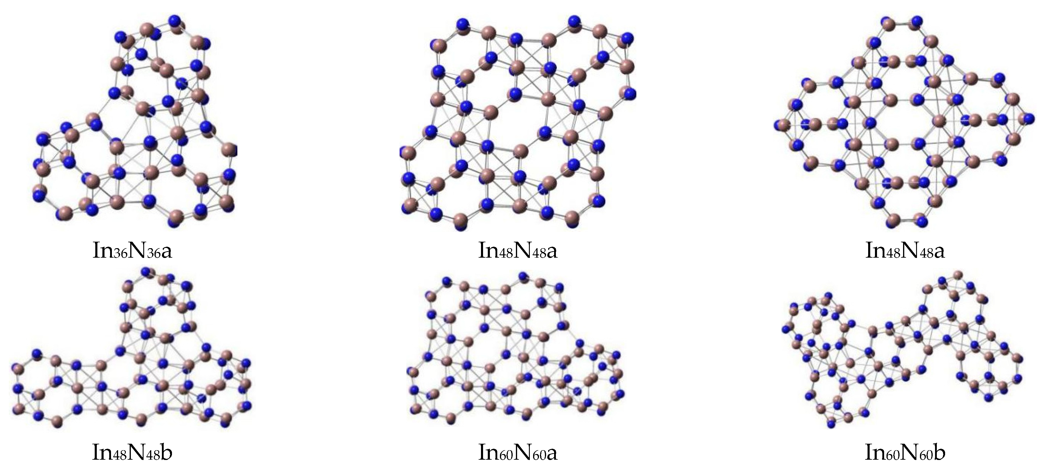
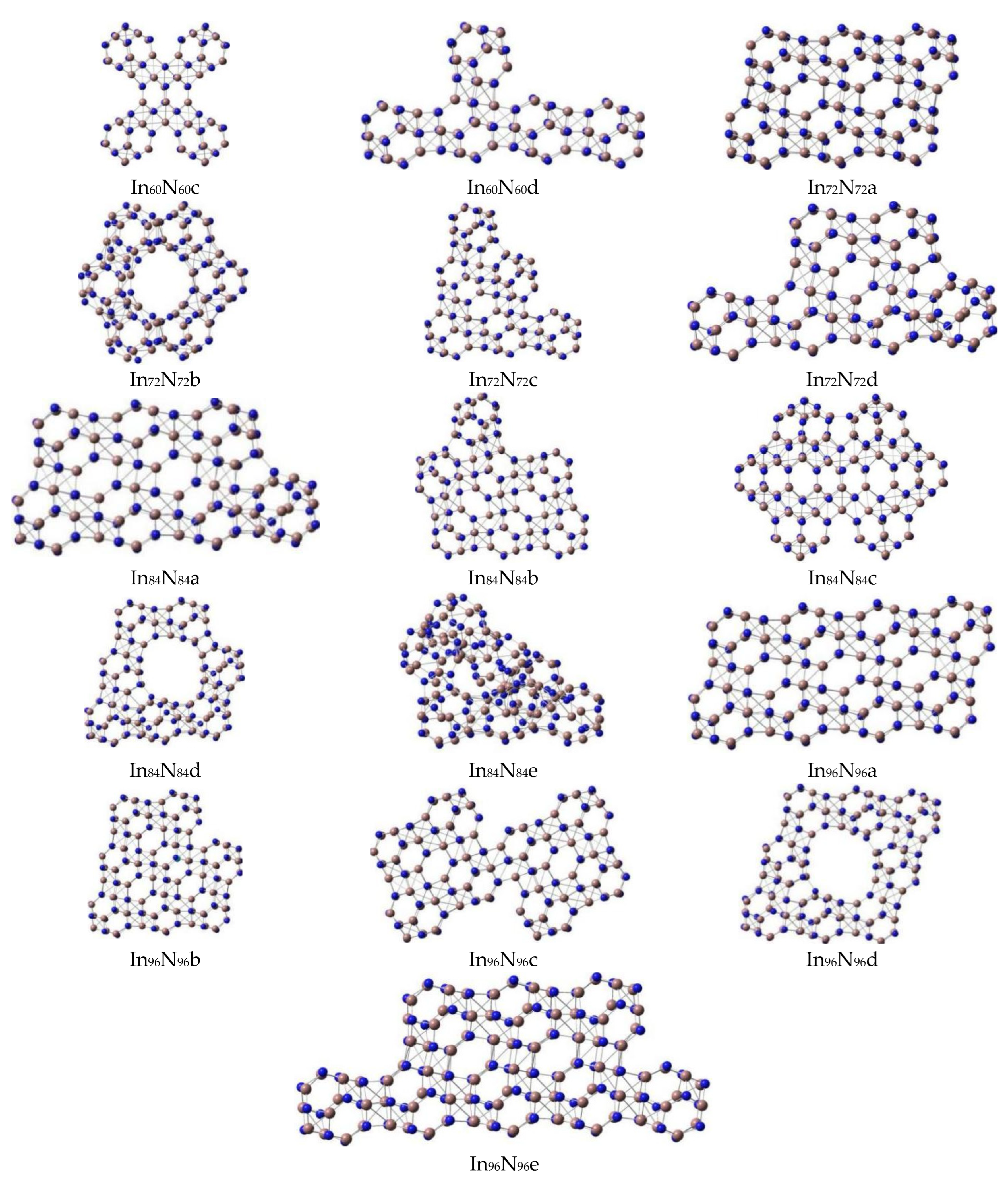
3.1. Geometries and Stabilities

In order to provide an accurate understanding of the geometrical and electronic properties of (InN)12n nanosheets with n = 1–8 (Figure 1 and Table 1) and (InN)12n nanowires with n = 1–9 (Table 2 and Figure 2), beginning with the predictions of the accurate geometrical forms of (InN)12n (n = 1–9) nanoclusters is required. Thus, the stable In12N12 unit was selected as an ideal building block [9] for designing various possible initial geometries of self-assembled (InN)12n nanowires and nanosheets.
All possible geometries of (InN)12n (n = 1–9) nanowires and (InN)12n (n = 1–8) nanosheets were optimized at the PBE1PBE level with a size in the regions of 5.1~63.4 Å. The (InN)12n (n = 1–9) nanoclusters (nanosheets and nanowires) were composed of many stable individual (InN)12 units (Figure 1 and Figure 2) connected by hexagonal prisms formed by six-membered rings in different (InN)12 units. In particular, the stable geometries of the (InN)12n (n = 1–9) nanowires formed by self-assembly of a number of (InN)12 units (Figure 2) were optimized to be stable linear forms with zero dipole moments and higher point group symmetry (Table 2).
According to the calculated dipole moment of the In24N24 unit in Table 1, the optimized geometry of the In24N24 nanowire is presented as a linear structure, which was composed of two (InN)12 units. The N-In bond lengths in each (InN)12 unit of In24N24 nanowire were predicted to be 2.27 (four-membered ring) and 2.12 Å (six-membered ring). The In-N connecting distance between two (InN)12 units was 2.14 Å, and these values demonstrate that the stable geometry of each (InN)12 unit in the In24N24 nanowire was slightly changed under the interactions between two (InN)12 units after both (InN)12 units were combined. In particular, the stable (InN)12 geometry near the connecting part deviated slightly from its original individual form. However, the (InN)12 geometry, which was not involved in the connecting section, being 2.01 (or 2.00) Å for hexagons (six-member rings) and 2.09 Å for squares (four-member rings), maintained the geometrical form of its individual isolated (InN)12 unit. As far as the In36N36 isomers are concerned, two possible In36N36 isomers were considered and optimized as stable structures. The energetically favorable In36N36 geometry with a zero dipole moment was the linear form, which was lower in total energy than the triangle form and slightly deformed the higher point-group symmetry, reflecting that linear In36N36 geometry was the most stable one. The linear geometry of In36N36a is shown in Figure 2, and its total energy was higher than that of In36N36b, which is shown in Figure 1.
A variety of possible initial geometrical forms were optimized for In48N48 geometries. The four stable In48N48 geometries are illustrated in Figure 1 and Figure 2. For the optimized In48N48 geometries, the most stable rhombus In48N48a geometry was selected as the ground state and its dipole moment was calculated to be 0.01 Debye. The In48N48b was seen to be an (InN)12 cage capped on the linear In36N36 geometry. This geometry was slightly bigger in total energy than the linear In48N48c cluster. After one (InN)12 unit was capped on the In48N48a rhombus geometry, the newly formed nonlinear In60N60a nanosheet was generated, which was the lowest-energy structure. The In60N60b, In60N60c, and In60N60d isomers were yielded by inserting one In12N12 unit into the In48N48b structure. Moreover, the total energies of these geometries were higher than those of the linear In60N60e isomer, reflecting that the linear In60N60e structure was more stable than those of the In60N60b, In60N60c, and In60N60d isomers; however, it was less stable than that of the In60N60a nanosheet.
According to the optimized stable In72N72 geometries, the newly formed rhombus In72N72a geometry was the most stable geometry, and its dipole moment was predicted to be 0.01 Debye, which was generated from the In60N60a nanosheets via the addition of a new In12N12 unit; moreover, this geometry deviated slightly to the higher point-group symmetry. It should be mentioned that the linear In72N72e geometry was less stable energetically than the In72N72b, In72N72c, In72N72d, and In72N72e geometries.
Following these procedures, In84N84a and In84N84b isomers, which were generated from the In72N72a geometry, were investigated. As seen in Table 1 and Table 2, it is exhibited that the calculated total energy difference between In84N84a and In84N84b was 0.092 eV, and the total energy of the In84N84b geometry was slightly higher than that of In84N84a. Consequently, In84N84a was more stable than the In84N84b nanosheet, and the In84N84a nanosheet was confirmed to be the most stable geometry. In particular, the In84N84c nanosheet was obtained by combining two In48N48a units together, and it was less stable than the In84N84b nanosheet. The In84N84e nanosheet, which deformed the plane-like form, was only higher in total energy than the linear In84N84f geometry. However, the energy gap of the linear In84N84f geometry (2.60 eV) was bigger than that (2.45 eV) of the most stable In84N84a structure. Eventually, the distinct characteristic of the energy gap of linear geometry was increased with the size of the cluster being extended. In particular, an energy gap of an In84N84f nanowire being 2.60 eV is in the range suitable for optoelectronic devices that emit in the visible region. The formation of semiconductor nanowires with an energy gap in the visible region of 1.62~3.11 eV has potential applications in the fields of nanophotonics, nanoelectronics, and medicine, which are consistent with the experimental results.
All possible In96N96 isomers were considered, and six possible In96N96 nanoclusters were optimized to be stable geometries. The stable In96N96a nanosheet was generated by capping one In12N12 unit on the In84N84a or In84N84b isomers. The In96N96a nanosheet with a dipole moment of 0.04 Debye was lower in total energy by 1.104 eV than the In96N96b nanosheet. Consequently, the In96N96a nanosheet was more stable than the In96N96b nanosheet; the formation of the In96N96c nanosheet was based on the combination of two In48N48 units, and the In96N96c nanosheet was less stable than both In84N84a and the In84N84b isomers. The interesting rhombus In96N96d nanosheet yielded a big hole in the center; this stable isomer can be suitable for hosting new clusters or molecules for application in porous nanomaterials. According to the calculated results in Table 1 and Figure 1, the In96N96e nanosheet was also obtained from the In84N84a nanosheet, and this structure was more stable than both the In96N96c and the In96N96d nanosheets. Finally, the linear In96N96 geometry is mentioned, and this isomer had the same energy gap (2.60 eV) as the linear In72N72 and In84N84 isomers (Figure 2 and Table 2). In particular, the energy gap of the In108N108 nanowire was determined to be 2.59 eV, which was slightly smaller than those of the In72N72, In84N84, and In96N96 nanowires.

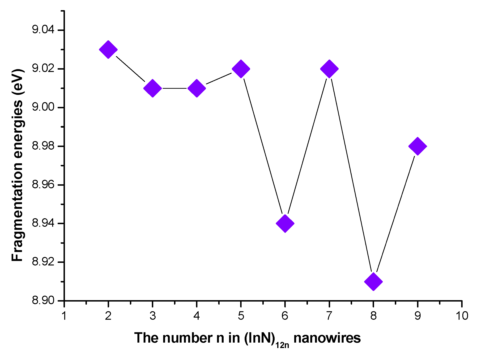
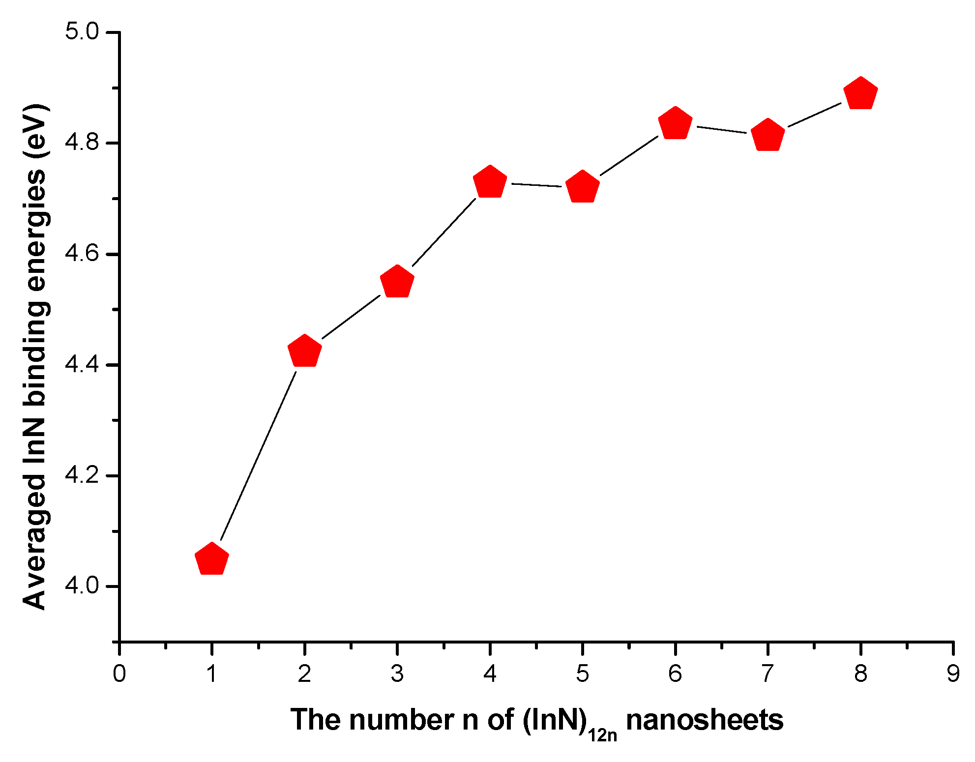
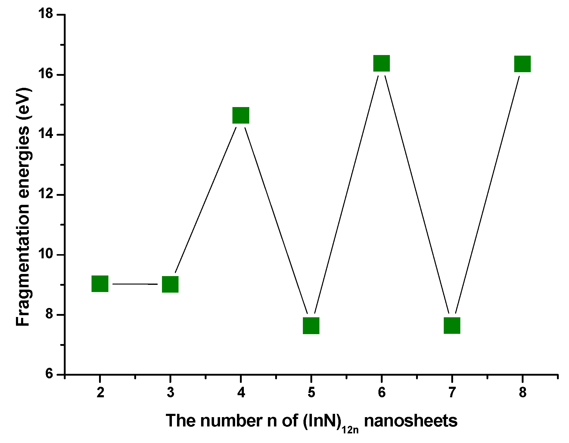
3.2. Relative Stabilities
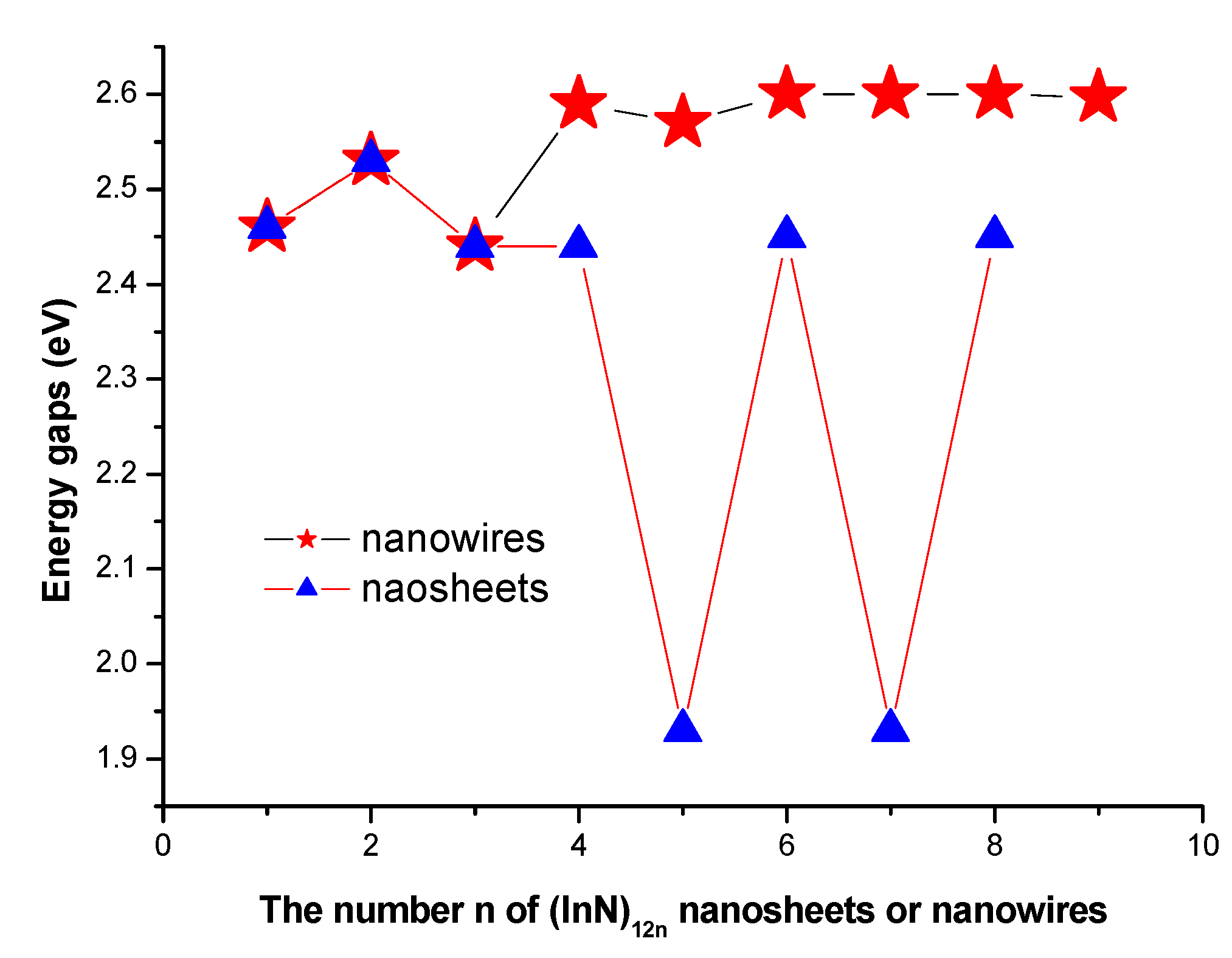
The relative stabilities of (InN)12n nanoclusters consisting of different In and N atoms were investigated based on the average InN diatomic binding energies (Eb(n)) as well as the calculated fragmentation energies (D(n, n−1)), which are defined as
E b ( n ) = 12 n E T ( I n N ) E T [ ( I n N ) 12 n ] 12 n
D ( n , n 1 ) = E T [ ( I n N ) 12 ( n 1 ) ] + E T ( I n N ) 12 E T [ ( I n N ) 12 n ]
where ET[(InN)12n], ET(InN), and ET[(InN)12(n−1)] are the calculated total energies of the respective (InN)12n and (InN)12(n−1) nanoclusters, together with the InN dimer, with zero-point vibration energies being taken into accounts. The total energy of the InN diatom was predicted to be −56.424257 Hartree.
Although the (InN)12n nanowires were relative weak in stability compared to the (InN)12n nanosheets, the promising potential applicability of (InN)12n nanowires is very unique because a newly type of semiconductor (InN)12n nanowire in a radius within the region of a few tens of nanometers is considered to be the ideal candidate for further developing optoelectronic and electronic nanodevices. Thus, the relative stabilities of (InN)12n nanowires are considered and discussed in detail in this study due to their unique semiconductor properties. According to our calculated relative stabilities of (InN)12n nanowires connected by six-membered rings, the average InN diatomic binding energy (Eb(n)) of (InN)12n nanowires increased continually to the maximum value of 4.714 eV when the size of (InN)12n nanowires varied from n = 1 to n = 9. In order to demonstrate the reliability of the averaged InN diatomic binding energies of (InN)12n nanowires, the fragmentation energies (D(n,n−1)) of (InN)12n nanowires were also taken into accounts. As seen from the curves of the fragmentation energies as a function of size (Figure 3 for (InN)12n nanowires), the apparent tendency for (InN)12n nanowires was that their fragmentation energies decreased as the size of (InN)12n nanowires varied from n = 1 to n = 9 (Figure 3). In general, the calculated values of the fragmentation energies for the (InN)12n nanowires exhibited an alternating even–odd oscillation, with the even-numbered (InN)12n nanowire (n is even) being smaller in fragmentation energy than its odd-numbered neighboring (InN)12n nanowires (n is odd), reflecting that the odd-numbered semiconductor (InN)12n nanowires had stronger stability than their neighboring even-numbered semiconductor (InN)12n nanowires.
The average InN diatomic binding energies of the stable (InN)12n nanoclusters (including nanowires and nanosheets) are listed in Table 1 and Table 2 and shown in Figure 4. Based on the calculated average InN diatomic binding energy for (InN)12n nanoclusters, the magic numbers of stabilities for (InN)12n nanoclusters were assigned at n = 2, 4, 6, and 8, reflecting that the even-membered semiconductor (InN)12n nanoclusters (n is even) were apparently more stable compared with their neighboring odd-numbered n in (InN)12n (n > 2) units.
Based on the calculated D(n,n−1) of (InN)12n nanoclusters (nanowires and nanosheets) shown in the curve in Figure 5, the calculated fragmentation energies for (InN)12n nanoclusters had the same tendency as those of (InN)12n nanowires mentioned above, with the calculated values of fragmentation energies for (InN)12n nanoclusters generally showing an appealing even–odd oscillation. On the contrary, the even-numbered semiconductor (InN)12n nanoclusters (where n is even) had higher fragmentation energy than the odd-numbered ones, suggesting that the even-numbered nano-size (InN)12n (where n is even) clusters had stronger stability compared with their odd-numbered (InN)12n neighbors. The remarkable peaks were n = 4, 6, and 8. Interestingly, the In72N72 and In96N96 nanosheets, with n = 6 and 8, respectively, were composed of individual (InN)48 (n = 4) units, indicating that In72N72 and In96N96 nanosheets were generated by the primarily newly formed In48N48 nanosheets; thus, one can infer that even-numbered (InN)12n can be detected more easily with mass spectroscopy experimental measurements with remarkably large abundances than the neighboring odd-numbered (InN)12n ones. More importantly, the (InN)12n nanosheet with n = 4 was assigned as a newly formed self-assembled building block for new film nanosheets. Eventually, the (InN)48a nanosheet was selected as the newly formed building block for self-assembled (InN)12n semiconductor film nanosheets (or nanomembranes), which have an important application in microelectronic and optoelectronic nanodevices. They can form the magnetic nanomembrane after magnetic metal atoms or ions are inserted in a suitable hole in (InN)12n nanosheets.

3.3. HOMO-LUMO Gaps

The electronic properties of self-assembled (InN)12n nanoclusters (including both nanowires and nanosheets) associated with the calculated energy gap values between HOMO (the highest occupied molecular orbital level) and LUMO (the lowest unoccupied molecular orbital level) were investigated. The predicted HOMO-LUMO energy gaps of (InN)12n nanoclusters are summarized in Table 1 and Table 2 and shown in Figure 6.
Based on a theoretical point of view, the advantages of (InN)12n nanowires are that they are ideal models for further investigation and development of optoelectronic and electronic nanodevices. In order to reveal the geometrical and electronic properties of (InN)12n nanowires, DFT studies were performed. According to the calculated energy gaps of (InN)12n nanowires listed in Table 1 and shown in Figure 6, it is obvious that the obtained energy gap values of (InN)12n nanowires were oscillatory, increasing at the small size and finally reaching a maximum of 2.60 eV at the large size region of n = 9. Obviously, the calculated energy gap values of (InN)12n nanowires connected by six-membered rings varied slightly when the size of (InN)12n nanowires changed from n = 1 to n = 9. This varying tendency of the energy gaps in semiconductor (InN)12n (n = 1–9) nanowires is actually consistent with that of inner hollow InN nanoclusters [9]. Therefore, the (InN)12n nanowires almost maintained the energy gap properties of an individual In12N12 unit; consequently, the variations in the energy gaps in (InN)12n (n = 1–9) nanowires were indeed small when the size n of (InN)12n nanowires varied from n = 1 to n = 9. The varying tendency of the energy gaps in (InN)12n nanowires may have directly led to a quantum size effect. Moreover, the slight variations in the energy gaps for the semiconductor (InN)12n (n = 1–9) nanowires revealed that the (InN)12n nanowires possessed the analogue characteristics and properties of individual (InN)12 units [9]. The calculated energy gaps of the semiconductor (InN)12n nanowires at the approved 2.44~2.60 eV regions were obviously within the visible light region, indicating that the size of the nanowires generated small influences on their energy gaps and reflecting that this kind of (InN)12n nanowire can give rise to the widespread applications in the fields of nanophotonics and nanoelectronics. Moreover, the unique HOMO-LUMO properties of semiconductor (InN)12n nanowires are receiving extremely noteworthy attention and promoted research, resulting in the opportunity for the widespread development of nanodevices and surface sciences.
The energy gap values for (InN)12n nanoclusters (nanowires and nanoclusters) were calculated and are shown in Figure 6. According to the calculated energy gap values of (InN)12n nanoclusters, it is exhibited that the obtained energy gaps of (InN)12n nanosheets within the range of 1.93~2.53 eV depended on the varied size of the nanosheets, reflecting that cluster-assembled (InN)12n nanosheets are good semiconductor optoelectronic or energy nanomaterials and give rise to attractive optical and electrooptical properties. The variation in the HOMO-LUMO gaps of (InN)12n nanowires was smaller than that of (InN)12n nanosheets as their size was extended. The HOMO-LUMO gaps (energy gaps) of even-numbered (InN)12n nanosheets were bigger than those of the neighboring odd-numbered (InN)12n nanosheets. The maximum value of the energy gap (2.53 eV) was assigned as n = 2, and the corresponding (InN)24 nanosheet had the strongest chemical stability. The minimum values of energy gaps (1.93 eV) were assigned as n = 5 and n = 7, and the (InN)60 and (InN)72 nanosheets had the weakest chemical stability and the strongest chemical activity, respectively. Moreover, the relative stabilities of (InN)12n nanosheets with n = 5 and n = 7 were weakened compared to the neighboring (InN)12n nanosheets in that their nanostructures could be elucidated as smaller energy gaps with stronger chemical activity, reflecting that the surfaces of the (InN)12n nanosheets with n = 5 and n = 7 could react easily with a new (InN)12 unit, and stable (InN)12(n+1) nanosheets were achieved. This process is a cluster–cluster chemical reaction. In fact, the growth and formation of new nanoclusters (nanosheets and nanowires) are deeply involved in the catalytic process; in the other words, the cluster-assembled nanoclusters (nanosheets and nanowires) on the surface of film actually undergo chemical processes. Thus, (InN)12n with n = 4, 6, and 8 had remarkably larger abundances in experimental measurements due to their chemical stabilities. This finding is consistent with our discussions on relative stabilities in this manuscript. Moreover, the energy gaps of (InN)12n nanosheets are more favorable for optoelectronic applications than the reported experimental and theoretical findings [14,15,16,17]. These dimensionally uniform self-assembled (InN)12n nanosheets or nanowires may surmount the difficulties of lower efficiency, lower power, and lower quantum effect in monolayer (InN)12n nanosheets.

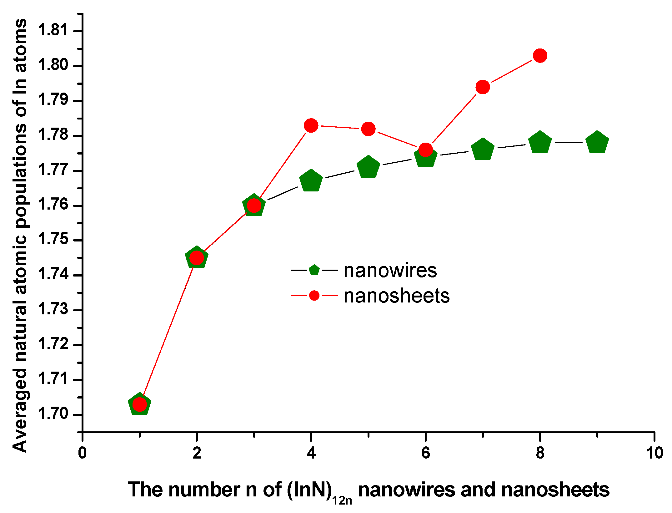
3.4. Natural Charge Population Analysis

The average natural atomic charge populations of indium atoms in the (InN)12n nanowires and nanosheets were obtained at the PBE1PBE level. The calculated average natural atomic charge populations for indium atoms are plotted in Figure 7. Based on the average natural atomic charge populations of indium atoms for all sizes of (InN)12n nanoclusters (including nanowires and nanosheets) tabulated in Table 1 and Table 2, it is evident that the charges in the self-assembled (InN)12n nanoclusters were transferred from the indium atoms to their neighboring nitrogen atoms, reflecting that the surface In atom in (InN)12n nanoclusters behaved like a Lewis acid site, whereas the electronegative nitrogen atoms behaved as a Lewis base site, and that they are appropriate sites for possible carbonylation by a CO2 molecule. The In and N atoms in the (InN)12n nanoclusters were chemically bonded with oxygen and carbon atoms, respectively, in CO2. Thus, (InN)12n nanoclusters are suitable for decomposing a CO2 molecule. As can be seen from Table 1 and Table 2 and Figure 7, there was an increasing trend of the average natural atomic charge population of indium atoms in (InN)12n nanoclusters with the increasing size of (InN)12n nanoclusters; the electronic charges in the N atoms originated from the neighboring In atoms. As far as the average natural atomic charge populations of indium atoms in (InN)12n nanowires are concerned, the maximum average natural atomic charge population values of In atoms of 1.774 and 1.778 corresponded to two remarkable peaks of (InN)12n nanowires with n = 6 and n = 8, respectively, at the curve in Figure 7. However, the local maximum average natural atomic charge population values for indium atoms in (InN)12n nanosheets of 1.783 and 1.803 corresponded to two remarkable peaks with n = 4 and n = 8, respectively, in Figure 7. Electrostatic interactions among all In and N atoms in (InN)12n nanoclusters resulting from charge transfers increased when the size of (InN)12n nanoclusters increased; therefore, the electrostatic interaction enhanced the stabilities of (InN)12n nanoclusters. Furthermore, the ionic bonding formed between the In and N atoms in (InN)12n nanowires or nanosheets eventually enhanced the stabilities of (InN)12n nanowires or nanosheets.

4. Conclusions

As for the (InN)12n nanoclusters consisting of numerous In12N12 units that were connected by six-membered rings, a series of (InN)12n nanowires or nanosheets was taken into account and their molecular structures and properties were elucidated and investigated at the PBE1PBE level. According to the calculated average InN diatomic binding energy and fragmentation energy, the relative stabilities of (InN)12n nanoclusters (nanowires and nanosheets) were studied, exhibiting that the even-numbered (InN)12n nanoclusters were obviously stronger in stability than their odd-numbered (InN)12n neighbors. The remarkable peaks were shown at n = 4, 6, and 8. Interestingly, the most stable In72N72 and In96N96 nanosheets consisted of (InN)48 nanosheets (n = 4); consequently, the (InN)48 nanosheet was confirmed to be a newly formed elemental building unit for cluster-assembled nanoscale film materials. With the nanowire size increasing from n = 1 to n = 9, a number of changes in the energy gaps of the (InN)12n nanowires were noted. Interestingly, the HOMO-LUMO gaps of (InN)12n nanowires at the region of 2.44~2.60 eV were within the visible light region. Furthermore, the slight variation in HOMO-LUMO gaps for (InN)12n nanowires reflect that (InN)12n nanowires maintained their property of an individual (InN)12 unit and reveal an important implication for the development of nanodevice prototypes. In summary, the energy gaps for (InN)12n nanosheets and nanowires were calculated, and the gaps of even-numbered (InN)12n nanoclusters were bigger compared with those of their odd-numbered (InN)12n neighbors. In addition, the obtained averaged natural atomic populations of In atoms in (InN)12n nanowires or nanosheets exhibited that charge transfers, together with ionic bonding, generally increased when the size of (InN)12n nanoclusters increased, and ionic bonding in (InN)12n nanoclusters existed with covalent bonding. The obtained charge transfers in (InN)12n nanoclusters reflect that the In atoms of (InN)12n nanoclusters behaved like a Lewis acid site, whereas the electronegative N atoms acted like a Lewis base site, and they can be appropriate sites for possible carbonylation of CO2 molecules.

Author Contributions

Conceptualization, R.Z.; methodology, R.Z., H.Z. and F.L.; software, R.Z.; validation, R.Z.; formal analysis, R.Z.; investigation, R.Z. and J.-G.H.; resources, R.Z.; data curation, R.Z. and R.C.; writing—original draft preparation, R.Z.; writing—review and editing, J.-G.H.; visualization, R.Z. and R.C.; supervision, J.-G.H.; project administration, R.Z. and J.-G.H.; funding acquisition, R.Z. All authors have read and agreed to the published version of the manuscript.

Funding

This research received no external funding.

Institutional Review Board Statement

Not applicable.

Informed Consent Statement

Not applicable.

Data Availability Statement

The data available are published the Tables of this article.

Acknowledgments

All computations were performed in the Supercomputing Center of the University of Science and Technology of China.

Conflicts of Interest

The authors declare no conflict of interest.

References

  1. Jimenez-Izal, E.; Ugalde, J.M.; Matxain, J.M. Nanocluster-Assembled Materials, Computational Modeling of Inorganic Nanomaterials; Taylor & Francis Group, LLC: New York, NY, USA, 2016. [Google Scholar]
  2. Gu, Y.B.; Xu, N.X.; Lin, M.H.; Tan, K. Structures, stabilities and properties of hollow (Al2O3)n clusters (n = 10, 12, 16, 18, 24 and 33): Studied with density functional theory. Comput. Theor. Chem. 2015, 1063, 29–34. [Google Scholar]
  3. Yeganeh, M.; Kafi, F.; Boochani, A. Thermoelectric properties of InN graphene-like nanosheet: A first principle study. Micro. Nanostruct. 2020, 138, 106367. [Google Scholar]
  4. Castillo, R.M.d.; Salcedo, E.; Martínez, A.; Ramos, E.; Sansores, L.E. Electronic Peculiarities of a Self-Assembled M12L24 Nanoball (M = Pd+2, Cr, or Mo). Molecules 2019, 24, 771. [Google Scholar] [CrossRef] [PubMed]
  5. Orek, C.; Keser, S.; Kaygili, O.; Zuchowski, P.; Bulut, N. Structures and optical properties of zinc oxide nanoclusters: A combined experimental and theoretical approach. J. Mol. Model. 2023, 29, 227. [Google Scholar]
  6. Duan, X.; Huang, Y.; Cui, Y.; Wang, J.; Lieber, C.M. Indium phosphide nanowires as building blocks for nanoscale electronic and optoelectronic devices. Nature 2001, 409, 66–69. [Google Scholar] [CrossRef]
  7. Zhao, R.N.; Chen, R.; Li, Q.; Duan, Y.H. Geometries, stabilities and electronic properties of photo sensitized (CdS)2n (n = 5–27) nanoclusters. J. Alloy Compd. 2018, 762, 754–762. [Google Scholar]
  8. Zhao, R.N.; Chen, R.; Han, J.G. Geometrical and electronic properties of the plane-like selfassembled structured (In12N12)n (n = 1–9) nanomaterials based on In12N12 cages connecting with four-membered rings. Micropor. Mesopor. Mat. 2021, 318, 111041. [Google Scholar]
  9. Zhao, R.N.; Han, J.G.; Duan, Y.H. A density functional prediction of geometries and stabilities and electronic properties of nanosize cagelike (InN)2n (n = 6–27, 45, 54) semiconducor material. Adv. Theor. Simul. 2018, 1, 1800001. [Google Scholar] [CrossRef]
  10. Inushima, T. Electronic structure of superconducting InN. Sci. Technol. Adv. Mater. 2006, 7, S112–S116. [Google Scholar]
  11. Zhang, Q.F.; Wang, L.S.; Zheng, H.F.; Su, A.M.; Liu, X.; Xie, X.J.; Chen, Y.Z.; Peng, D.L. Effect of in situ low-temperature annealing on anomalous Hall effect in Co nanocluster-assembled granular film. J. Alloy Compd. 2018, 748, 922–928. [Google Scholar]
  12. Zhao, M.; Xia, Y.; Liu, X.; Tan, Z.; Huang, B.; Song, C.; Mei, L. First-Principles Calculations of AlN Nanowires and Nanotubes:  Atomic Structures, Energetics, and Surface State. J. Phys. Chem. B 2006, 110, 8764–8768. [Google Scholar] [CrossRef] [PubMed]
  13. Romero, C.P.; Volodin, A.; Vece, M.D.; Paddubrouskaya, H.; Wang, H.; Vantomme, A.; Haesendonck, C.V.; Lievens, P. Passivation of cobalt nanocluster assembled thin films with hydrogen. Thin Solid Film. 2012, 520, 5584–5588. [Google Scholar] [CrossRef]
  14. Farzan, M.; Elahi, S.M.; Salehi, H.; Abolhassani, M.R. An investigation of electronic and optical properties of InN nanosheet by first principle study. Opt. Commun. 2017, 395, 293. [Google Scholar] [CrossRef]
  15. Podlipskas, Z.; Jurkevicius, J.; Kadys, A.; Kolenda, M.; Kovalevskij, V.; Dobrovolskas, D.; Aleksiejunas, R.; Tamulaitis, G. Extreme radiation resistance in InN. J. Alloy Compd. 2019, 789, 48–55. [Google Scholar] [CrossRef]
  16. Nagai, K.; Akiyama, T.; Nakamura, K.; Ito, T. A Simple Approach to Growth Mode of InN and InGaN Thin Films on GaN(0001) Substrate. ECS Trans. 2020, 98, 155–164. [Google Scholar] [CrossRef]
  17. An, Y.; He, Y.; Wei, H.; Liu, S.; Li, M.; Song, Y.; Qiu, P.; Rehman, A.; Zheng, X.; Peng, M. Metallic indium segregation control of InN thin films grown on Si(100) by plasma-enhanced atomic layer deposition. Results Phys. 2019, 12, 804–809. [Google Scholar] [CrossRef]
  18. Ma, S.; He, C.; Sun, L.Z.; Lin, H.; Li, Y.; Zhang, K.W. Stability of two-dimensional PN monolayer sheets and their electronic properties. Phys. Chem. Chem. Phys. 2015, 17, 32009–32015. [Google Scholar] [CrossRef]
  19. Dong, L.H.; Liu, Y.; Zhuo, Y.J.; Chu, Y.; Wang, Y.P. Effect of alien cations on the growth mode and self-assemble fashion of ZnO nanostructures. J. Alloy Compd. 2010, 509, 2021–2030. [Google Scholar] [CrossRef]
  20. Wu, X.; Li, K.; Wang, H. Facile synthesis of ZnS nanostructured spheres and their photocatalytic properties. J. Alloy Compd. 2009, 487, 537–544. [Google Scholar] [CrossRef]
  21. Zhang, Z.R.; Chai, C.; Song, Y.; Kong, L.; Yang, Y. A DFT study on physical properties of III-V compounds (AlN, GaN, AlP, and GaP) in the P3(1)21 phase. Mater. Res. Express 2021, 8, 025908. [Google Scholar] [CrossRef]
  22. Ernzerhof, M.; Scuseria, G.E. Assessment of the Perdew—Burke—Ernzerhof exchange-correlation functional. J. Chem. Phys. 1999, 110, 5029–5036. [Google Scholar]
  23. Frisch, M.J.; Trucks, G.W.; Schlegel, H.B.; Scuseria, G.E.; Robb, M.A.; Cheeseman, J.R.; Scalmani, G.; Barone, V.; Mennucci, B.; Petersson, G.A.; et al. Gaussian09; Gaussian, Inc.: Wallingford, CT, USA, 2009. [Google Scholar]
  24. Adamo, C.; Barone, V. Toward Reliable Density Functional Methods without Adjustable Parameters: The PBE0 Model. J. Chem. Phys. 1999, 110, 6158–6170. [Google Scholar] [CrossRef]
  25. Lin, L.H.; Yang, J.C.; Ning, H.M.; Hao, D.S.; Fan, H.W. Silicon–sodium binary clusters SinNa (n < 10) and their anions: Structures, thermochemistry, and electron affinities. Theochem 2008, 851, 197–206. [Google Scholar]
  26. Foster, E.; Wong, B.M. Nonempirically Tuned Range-Separated DFT Accurately Predicts Both Fundamental and Excitation Gaps in DNA and RNA Nucleobases. J. Chem. Theory Comput. 2012, 8, 2682–2687. [Google Scholar] [CrossRef]
  27. Wong, B.M.; Hsieh, T.H. Optoelectronic and Excitonic Properties of Oligoacenes: Substantial Improvements from Range-Separated Time-Dependent Density Functional Theory. J. Chem. Theory Comput. 2010, 6, 3704–3712. [Google Scholar] [CrossRef]
  28. Chang, C.; Lin, Y.; Niu, J.; Lour, W.; Tsai, J.; Liu, W. High-Performance AlGaN/GaN Enhancement-Mode High Electron Mobility Transistor by Two-Step Gate Recess and Electroless-Plating Approaches. Sci. Adv. Mater. 2021, 13, 30–35. [Google Scholar] [CrossRef]
Figure 1. The stable (InN)12n (n = 1–8) nanosheets with In12N12 units combined by their six-membered rings.
Molecules 28 07358 g001aMolecules 28 07358 g001b
Figure 2. The stable (In12N12)n (n = 1–9) nanowires connected by six-membered rings.
Molecules 28 07358 g002
Figure 3. The calculated fragmentation energies of (InN)12n nanowires.
Molecules 28 07358 g003
Figure 4. The calculated average InN diatomic binding energies of (InN)12n nanosheets.
Molecules 28 07358 g004
Figure 5. The calculated fragmentation energies of (InN)12n nanosheets.
Molecules 28 07358 g005
Figure 6. Energy gaps of (InN)12n nanowires or nanosheets as a function of the size of the nanowires or nanosheets, respectively.
Molecules 28 07358 g006
Figure 7. The average natural atomic populations of In atoms in (InN)12n nanosheets or nanowires.
Molecules 28 07358 g007
Table 1. Symmetry point groups (sym), average natural charges of In atoms (NC), dipole moment (Dip), isomers (iso), HOMO and LUMO gaps (Egap), average InN diatomic binding energies (Eb(n)), fragmentation energies (D(n, n–1)), lowest frequencies (Freq), and total energies (ET) of the most stable (InN)12n (n = 1–8) nanosheets. The stable geometries with In12N12 connected by six-membered rings.
SystemsSymIsoNCDipHOMOLUMOFreqEgapETEb(n)D(n, n−1)
DebyeHartreeHartreecm−1eVHartreeeVeV
In12N12Tha1.7030.00−0.22082−0.1305071.32.46−678.8763394.048
In24N24C1a1.7450.00−0.21941−0.1262635.52.53−1358.0844154.4249.03
In36N36S6a1.7600.01−0.22161−0.1317720.32.44−2037.2918264.5499.01
C1b1.7555.21−0.20426−0.1352126.4 −2037.234748
In48N48C1a1.7830.01−0.21476−0.1251527.82.44−2716.7064044.72914.645
C1b1.7645.61−0.20392−0.1339617.3 −2716.439412
In60N60C1a1.7824.96−0.20447−0.1336118.01.93−3395.8633204.7207.635
C1b1.5986.99−0.20888−0.1355210.2 −3395.596897
C1c1.7670.01−0.21577−0.1299810.9 −3395.595081
C1d1.7691.69−0.21508−0.1264210.0 −3395.652494
In72N72C1a1.7760.01−0.21425−0.1241518.42.45−4075.3415474.83516.377
C1b1.7765.02−0.23520−0.1228413.0 −4074.968946
C1c1.7816.22−0.20437−0.1334414.3 −4075.029513
C1d1.7834.05−0.20435−0.1335112.9 −4075.067931
In84N84C1a1.7944.88−0.20397−0.1330412.51.93−4754.4988714.8147.646
C1b1.7946.24−0.20149−0.1302815.2 −4754.495491
C1c1.6814.54−0.20426−0.1314513.2 −4754.455641
C1d1.7795.61−0.20761−0.128819.5 −4754.198775
C1e1.7767.18−0.20362−0.135579.9 −4754.111104
In96N96C1a1.8030.04−0.21351−0.1235612.02.45−5433.9766344.88916.365
C1b1.8021.91−0.21697−0.1261811.4 −5433.936053
C1c1.7910.20−0.21141−0.128036.8 −5433.655668
C1d1.7950.02−0.20682−0.1277710.6 −5433.515520
C1e1.7931.71−0.21340−0.125819.3 −5433.712151
Table 2. Symmetry point groups (sym), average natural charges of In atoms (NC), dipole moment (Dip), isomers (Iso), HOMO and LUMO gaps (Egap), average InN diatomic binding energies (Eb(n)), fragmentation energies (D(n, n−1)), lowest frequencies (Freq), and total energies (ET) of the most stable (InN)12n (n = 1–9) nanowires. The stable geometries with In12N12 connected by six-membered rings.
SystemsSymIsoNCDipHOMOLUMOFreqEgapETEb(n)D(n, n−1)
DebyeHartreeHartreecm−1eVHartreeeVeV
In12N12Tha1.7030.00−0.22082−0.1305071.32.46−678.8763394.048
In24N24C1a1.7450.00−0.21941−0.1262635.52.53−1358.0844154.4249.03
In36N36S6a1.7600.01−0.22161−0.1317720.32.44−2037.2918264.5499.01
In48N48C1c1.7670.00−0.21813−0.1232912.42.59−2716.4986274.6119.01
In60N60C1e1.7710.04−0.21783−0.122648.52.57−3395.7063524.6499.02
In72N72C1e1.7740.01−0.21772−0.122185.22.60−4074.9110664.6738.94
In84N84C1f1.7760.02−0.21755−0.121933.92.60−4754.1188334.6919.02
In96N96C1f1.7780.01−0.21741−0.121812.72.60−5433.3225074.7038.91
In108N108C1a1.7780.01−0.21724−0.121781.82.597−6112.5288884.7148.98
Disclaimer/Publisher’s Note: The statements, opinions and data contained in all publications are solely those of the individual author(s) and contributor(s) and not of MDPI and/or the editor(s). MDPI and/or the editor(s) disclaim responsibility for any injury to people or property resulting from any ideas, methods, instructions or products referred to in the content.

