Abstract
Defects in perovskite films are one of the main factors that affect the efficiency and stability of halide perovskite solar cells (PSCs). Uncoordinated ions (such as Pb2+, I−) act as trap states, causing the undesirable non-radiative recombination of photogenerated carriers. The formation of Lewis acid–base adducts in perovskite directly involves the crystallization process, which can effectively passivate defects. In this work, 4-(trifluoromethyl)-1H-imidazole (THI) was introduced into the perovskite precursor solution as a passivation agent. THI is a typical amphoteric compound that exhibits a strong Lewis base property due to its lone pair electrons. It coordinates with Lewis acid Pb2+, leading to the reduction in defect density and increase in crystallinity of perovskite films. Finally, the power conversion efficiency (PCE) of PSC increased from 16.49% to 18.97% due to the simultaneous enhancement of open-circuit voltage (VOC), short circuit current density (JSC) and fill factor (FF). After 30 days of storage, the PCE of the 0.16 THI PSC was maintained at 61.9% of its initial value, which was 44.3% for the control device. The working mechanism of THI was investigated. This work provides an attractive alternative method to passivate the defects in perovskite.
1. Introduction
In recent years, halide perovskite solar cells (PSCs) have developed rapidly, and their performance has achieved significant improvements. Their power conversion efficiency (PCE) has increased at an astonishing rate from the initial 3.8% to over 25% [1,2], which is close to that of the currently commercialized silicon-based solar cells, demonstrating the enormous commercialization prospects in the field of photovoltaics. The excellent performance of PSC is mainly due to the unique properties of halide perovskite, such as its high absorption coefficient, low binding energy, long carrier diffusion length and high carrier mobility. Meanwhile, halide perovskite thin films can be deposited through the low-temperature solution processing technology, exhibiting its great potential for flexible devices [3,4].
However, at present, PSCs face a serious challenge, which that the deep-energy-level defects in perovskite films severely limit their PCE and stability. The film quality of perovskite plays a vital role in achieving highly efficient PSCs. Despite great advances in high-quality perovskite, the inherently soft lattices of polycrystalline films deposited by the solution-processing technology present weak binding character, resulting in rich defects [5,6]. Defects were generated during the in situ crystallization of perovskite film, of which the deep-energy-level defects caused non-radiative recombination losses during device operation, leading to the performance degradation. Moreover, these defects can bring about ion migration under illumination or electric field, which reduces the stability of perovskite [7,8,9]. Therefore, it is necessary to eliminate the deep-energy-level defects in perovskite films to improve the performance of PSCs. Deep-energy-level defects in MAPbI3 thin films are mainly point defects, including uncoordinated Pb2+, uncoordinated halide ions, Pb clusters and Pb-I antisite defects [10,11]. Thus, forming chemical bonds is a promising way to eliminate uncoordinated Pb2+ or halide ions [12]. According to the soft material nature of perovskite, weak interactions such as coordination bonds, ion bonds, and hydrogen bonds are used, among which, coordination bonds based on Lewis acid–base theory are very promising [11]. Imidazole is a typical amphoteric compound, in which the nitrogen has a lone pair of electrons exhibiting strong basicity and weak acidity due to the combination of an acid proton with another nitrogen molecule. Thus, the imidazole group is likely to coordinate with Lewis acid and Lewis base defects, forming Lewis acid–base adducts. For example, imidazole was doped into the perovskite absorption layer to realize the reduction in defect density [13]; 4-iodo-1H-imidazole was introduced into the perovskite precursor solution to prevent defect formation, leading to a significant elevation in the open-circuit voltage (VOC) of PSC [14]; imidazolium iodide (ImI) applied on the surface of MAPbI3 passivated the iodide vacancies of the perovskite by occupying the vacant sides in the crystal lattice, which minimized recombination losses [15]; 4-imidazoleacetic acid hydrochloride (ImAcHCl) was employed to modify the surface of electron transport layer SnO2 [16], leading to the passivation of defects via interaction between imidazolium cation in ImAcHCl and iodide anion in perovskite; the surface modification of TiO2 was achieved using 1-butyl-3-methylimidazolium tetrafluoroborate, resulting in increased PCE and eliminated hysteresis in planar PSCs [17]; the incorporation of imidazole bromide functionalized graphene quantum dots (I-GQDs) on the surface of the electron transport layer not only reduced the interface defects but also improved the film quality of FAPbI3 perovskite [18].
In this study, imidazole derivative 4-(trifluoromethyl)-1H-imidazole (THI) was introduced into the perovskite precursor solution to passivate defects in the perovskite films. Due to its voluminous size, THI will not enter into the perovskite lattice but can act as an ionic. It was shown that THI-added perovskite films have better crystallinities and larger grain sizes, which effectively reduces the density of defect states and eliminates non-radiative recombination. The doping concentration of THI in the perovskite precursor solution was optimized, which was 0.16 wt%. The PCE of PSC was significantly enhanced from 16.49% of the control device to 18.97%. The work mechanism of THI was thoroughly investigated by using X-ray photoelectron spectroscopy (XPS), a scanning electron microscope (SEM) and an electrochemical impedance spectrum (EIS). This work provides an alternative passivate agent to passivate defects of perovskite film.
2. Results and Discussion
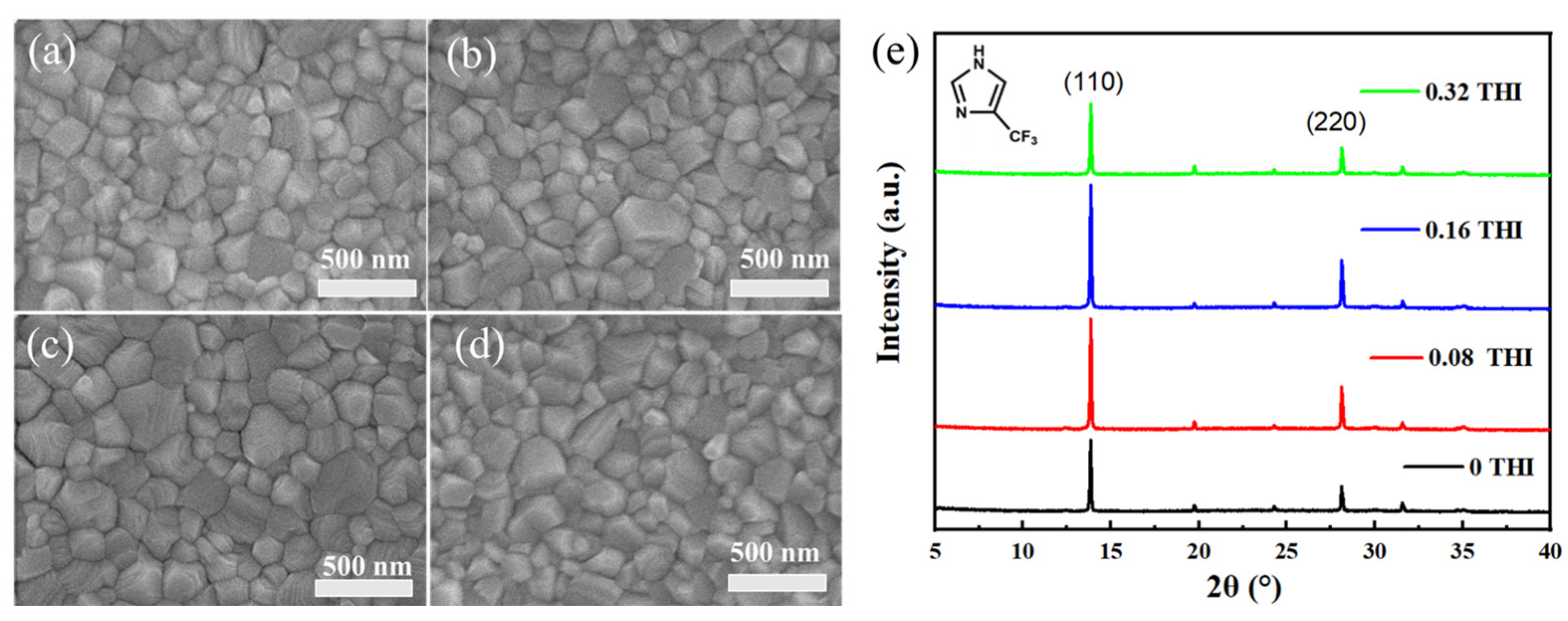
The effect of THI addition on the morphology of perovskite thin films was investigated, the SEM images of which are shown in Figure 1. The perovskite films prepared from different weight ratios of THI in the perovskite precursor solution (0 wt%, 0.08 wt%, 0.16 wt% and 0.32 wt%) were named 0 THI, 0.08 THI, 0.16 THI and 0.32 THI, respectively. It could be observed that all the perovskite films were dense and pinhole-free with full coverage on the substrate. But the grain sizes varied greatly, which were estimated using Nano Measure 1.2 software and are summarized in Table 1. It can be seen that the grain size of MAPbI3 thin films increased first and then decreased with the increasing doping ratio of THI from 0 wt%, 0.08 wt% and 0.16 wt% to 0.32 wt%. The mean grain size values of all THI-doped perovskite films were larger than that of the pristine film. The 0.16 THI perovskite film had the largest average grain size (223.78 nm), while that of the 0 THI perovskite films was 177.44 nm. The significantly increased grain size indicates that THI doping enhanced the crystallinity of the perovskite films.

Figure 1.
Top-view SEM images of perovskite films: (a) 0 THI, (b) 0.08 THI, (c) 0.16 THI and (d) 0.32 THI; (e) XRD patterns of perovskite films based on different concentration of THI; inside is the molecular structure of THI.

Table 1.
Grain size statistics, XRD peak intensity and FWHM values of diffraction peak of 13.90° for perovskite films with different doping ratios of THI.
X-ray diffraction (XRD) patterns were also collected to further study the crystal structure and crystallinity of perovskite films (Figure 1e); inside was the molecular structure of THI, which is also shown in Figure S1. All the XRD patterns show two significant peaks at 13.90° and 28.17°, corresponding to the (110) and (220) crystal planes of MAPbI3, respectively. This indicates that all MAPbI3 films had an orthorhombic crystal structure, and the addition of THI did not change the component of perovskite. Meanwhile, the intensity of the XRD peaks changed significantly after doping THI. In terms of the peak at 13.90°, the intensities of 0 THI, 0.08 THI, 0.16 THI and 0.32 THI perovskite films were 4605, 6940, 7831 and 4669, respectively. In addition, it was also found that the full width at half maximum (FWHM) of (110) diffraction peak (Table 1) was narrowed as a result of the THI doping. The uplifted peak intensity and narrowing of FWHM of XRD patterns indicate that THI doping enhanced the crystallinity of MAPbI3 films. The parabolic-shaped changing trend of peak intensity with the concentration increase in THI shows that 0.16 THI film had the strongest diffraction peak intensity. Thus, 0.16 wt% is the optimum doping concentration of THI in consideration of the crystallinity of the perovskite films. This result is in accordance with the SEM images of perovskite films.
The changes in the morphology of perovskite thin films are often accompanied by variations in their light absorbance. The ultraviolet–visible (UV-Vis) absorption spectra of perovskite films were measured, as shown in Figure 2a. The absorption spectra of MAPbI3 films with different THI doping concentrations all showed the same shapes with two distinct absorption peaks at 480 nm and 740 nm, indicating the unchanged crystal structure of MAPbI3 films, which is consistent with the XRD patterns. After doping THI, the absorbance of perovskite film was enhanced in the range of 400–700 nm, which can be attributed to the improved crystallinity of MAPbI3 films [19,20].
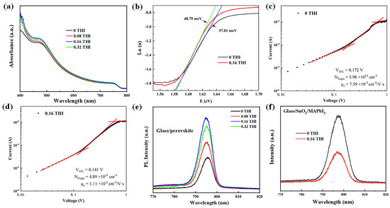
Figure 2.
(a) UV-Vis spectra of perovskite films based on different concentrations of THI in the perovskite precursor solution; (b) Urbach energy plot; J–V characterizations of electron-only devices with structure of ITO/SnO2 (20 nm) /MAPbI3 (260 nm)/PCBM (70 nm)/Ag (100 nm); (c) control device and (d) 0.16 THI device; (e) PL spectra of perovskite films on glass; (f) PL spectra of perovskite films on SnO2/glass.
The enlarged grain size of perovskite film means reduced defect density. Thus, Urbach energy (Eu) was calculated by fitting the exponential part of the absorption edge, according to Equation (1). The Urbach tail can reflect the defect density of perovskite [21], the change in which is consistent with the change in defect density. The greater the Urbach energy, the higher the defect density [22].
where α is the absorption coefficient and E is the photon energy. Eu value can be determined from the inverse of the slope of the linear fit of Ln(α) against E. The calculated Eu values are 57.01 meV and 48.79 meV for the pristine and 0.16 THI films, respectively. The decrease in the Eu value indicates the decrease in the defect density in the perovskite films after doping with THI [23].
The space-charge-limited current technique is often applied to electron- or hole-only devices to estimate the trap densities in semiconductors. Figure 2c,d show the dark I-V curves of electron-only devices in double logarithmic coordinates based on the pristine and 0.16 THI perovskite films. The structure of an electron-only device consists of indium tin oxide (ITO)/SnO2 (40 nm)/MAPbI3 (260 nm)/[6,6]-phenyl C61 butyric acid methyl ester (PCBM) (70 nm)/Ag (100 nm). The linear region at low bias voltage corresponds to the ohmic response. A trap-filling process is identified by the significant increase in the current injection in the intermediate region [24]. At high voltage, it is the space-charge-limited current (SCLC) region. The trap-filled-limited voltage (VTFL) refers to the kink point of the ohmic and TFL regions [25,26]. Typically, the density of defects () can be calculated using Equation (2) [27]:
where is the relative dielectric constant of MAPbI3 (ε = 32) [27], is the vacuum permittivity, L is the thickness of the perovskite film, e is the unit charge, and VTFL is the TFL voltage. It can be read from Figure 2c,d that the VTFL values of the control device and the 0.16 THI device are 0.172 V and 0.141 V, respectively. Accordingly, the calculated trap densities of the control device and the 0.16 THI device were 5.98 × 1015 cm−3 and 4.89 × 1015 cm−3, respectively. This further confirmed the diminishment of trap densities in perovskite film after the addition of THI.
The decrease in defect density is conducive to the transportation of charge carriers, which was verified by estimating the carrier mobility via Mottley–Gurney’s law (3) from the SCLC region [28]:
wherein Vb is the applied voltage; JD is the measured current density; μ is the mobility of charge carriers; L is the thickness of the perovskite light-absorbing layer; ε is the relative dielectric constant of MAPbI3 (ε = 32). The calculated electron mobility (μe) of the 0.16 THI device was 1.11 × 10⁻² cm2 V−1 s−1, which was much higher than the corresponding value of the control device: 7.59 × 10⁻³ cm2 V−1 s−1.
The steady-state photoluminescence (PL) spectra of perovskite films on glass were usually used to inspect the non-radiative recombination, which was shown in Figure 2e. The PL intensity of all THI-doped perovskite films was higher than that of the pristine one, implying the enhanced radiative recombination. Thus, the non-radiative recombination was reduced, which was mainly supported by the deep-level traps [29]. The 0.16 THI perovskite film had the highest PL intensity, suggesting the best film quality with the minimum trap density. This was in accordance with the SEM and XRD results. In addition, there was a small blue shift in the PL peak position after the addition of THI relative to the pristine film, which was also indicative of a reduction in defect density in the perovskite films [30]. Thus, the addition of THI passivated the defects in the MAPbI3 films. Moreover, PL is an effective method for studying the carrier dynamics at the interface. Effective carrier separation will cause a reduction in carrier radiative recombination. Thus, the lower PL intensity of the perovskite films on the charge transport layer indicates less carrier recombination, suggesting more effective carrier extraction. The PL spectra of the ITO/SnO2/MAPbI3 films were measured, where SnO2 was the electron transport layer, as shown in Figure 2f. The PL intensity of the 0.16 THI MAPbI3 film was lower than that of the pristine film, indicating the enhanced electron extraction after THI doping.
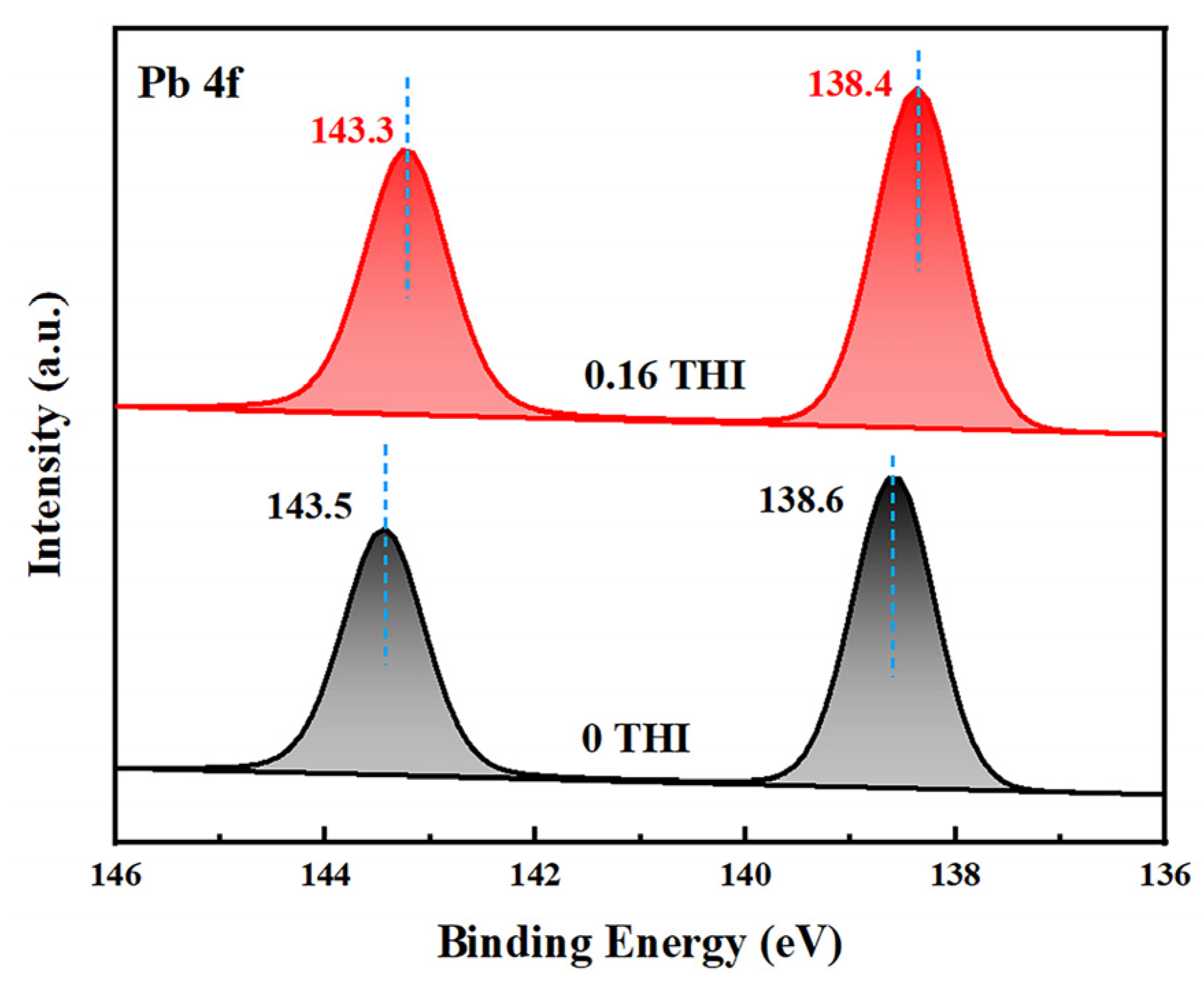
The above experimental results demonstrate that a THI additive in the precursor solution passivates the defects in perovskite films, resulting in increased light absorbance, enhanced PL intensity and more efficient electron extraction. To investigate the passivation mechanism of THI, X-ray photoelectron spectroscopy (XPS) was used to study the interaction between THI and MAPbI3. Figure 3 shows the XPS spectra of Pb 4f of the pristine and 0.16 THI MAPbI3 films. It shows two characteristic peaks corresponding to the spin–orbit splitting of the Pb 4f7/2 and Pb 4f5/2 components, respectively [31,32]. After doping 0.16 wt% THI, both the two peaks shifted downward, from 143.5 eV and 138.6 eV of the pristine film to 143.3 eV and 138.4 eV, respectively. The lower binding energy suggested the interaction between the imidazole group in THI and the uncoordinated Pb2+ in MAPbI3 [33]. In addition, the XPS spectra of I 3d of the pristine and 0.16 THI MAPbI3 films were also collected, as shown in Figure S1. The characteristic peaks of I 3d of the MAPbI3 film were 619.3 and 630.8 eV [32], which did not change after the addition of THI. This implies that there is no interaction between THI and I−, or the interaction is too weak to be detected. It can be ascribed to the weak Lewis acid property of THI.

Figure 3.
XPS spectra of Pb 4f of the pristine and 0.16 THI perovskite films.
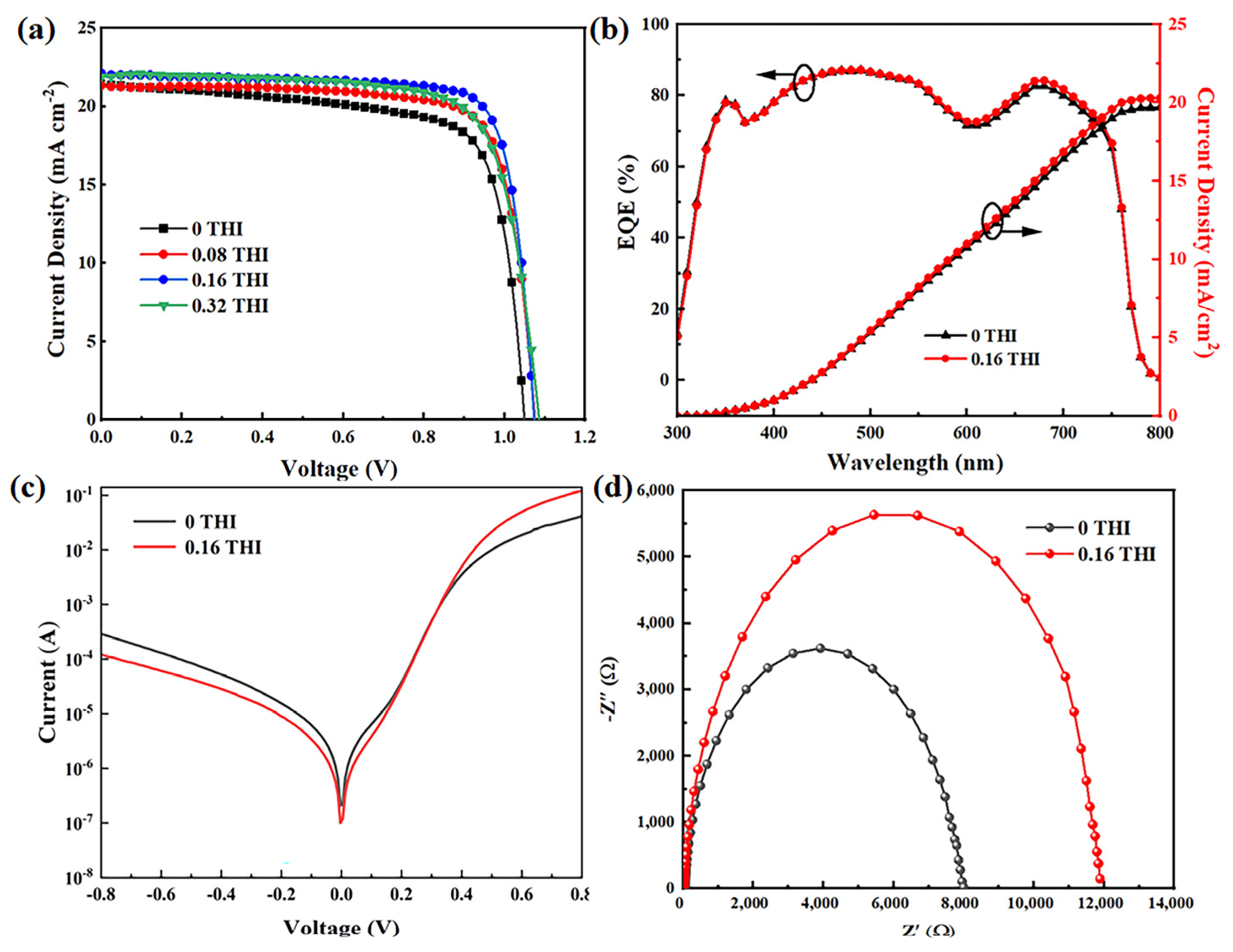
The effects of THI additives on the performance of PSCs were characterized by fabricating devices with structures of ITO/NiOx (20 nm)/MAPbI3 (260 nm)/PCBM (70 nm)/2,9-dimethyl-4,7-diphenyl-1,10-phenanthroline (BCP) (5 nm)/Ag (100 nm), which is illustrated in Figure S2. The current density–voltage (J–V) curves of PSCs based on perovskite films with different concentrations of THI are shown in Figure 4a, and the corresponding performance parameters are summarized in Table 2. It can be seen that the VOC, short circuit current density (JSC) and fill factor (FF) of PSCs were all increased after the addition of THI. With the concentration increase in THI, the performance of PSC increased first and then decreased. When the doping concentration of THI was 0.16 wt%, the device performance reached the maximum. The VOC, JSC and FF of the control device were 1.05 V, 21.39 mA cm−2 and 73.44%, respectively, which were 1.07 V, 22.04 mA cm−2 and 80.19% for the 0.16 THI-based PSC, resulting in an enhancement in PCE from 16.49% to 18.97%. The PCE statistics of PSCs are shown in Figure S3, which show narrow distributions for both the control and 0.16 THI devices. Shockley Read Hall (SRH) recombination is considered to be the dominant pathway leading to the VOC loss in PSC, which is mainly caused by deep-level defects in perovskite films [11]. Thus, the passivation of defects in perovskite films by adding THI led to the increase in the VOC of PSC. Incident photon-to-current efficiency (IPCE) data were collected to verify the increase in the JSC of PSCs, as shown in Figure 4b. The 0.16 THI PSC exhibited a stronger spectral response in the whole visible wavelength range compared with the control device. The integrated current density was 19.71 mA cm−2 and 20.30 mA cm−2 for the control and 0.16 THI device, respectively. The reduction in defects in perovskite films is beneficial for the transportation of charge carriers, which is the major factor that caused the improvement in the JSC of PSC.
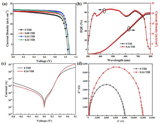
Figure 4.
(a) J−V curves of PSCs based on different THI doping concentrations; (b) IPCE curves of PSCs, (c) dark I-V curves and (d) Nyquist plots of EIS of the control and 0.16 THI devices.

Table 2.
Summary of detailed performances parameters of PSCs.
To investigate the charge carrier transport dynamic, the dark I-V and Nyquist plot of EIS of the control and 0.16 THI PSCs were collected. As shown in Figure 4c, at a negative voltage, the lower current of the 0.16 THI device compared with the control device suggested a smaller leakage current, which was in an inverse relationship with the shunt resistance (Rsh). At a high positive voltage, the current was in an inverse relationship with the series resistance (Rs). The larger current of the 0.16 THI device implied a smaller Rs, which resulted from the improved perovskite film with less defects [34]. Both the larger Rsh and smaller Rs corresponded to a higher FF [35]. Thus, the FF of PSC increased with the addition of THI.
In addition, EIS is a powerful tool to investigate properties of materials and electrode reactions. The Nyquist plots of EIS were depicted to obtain the composite resistance (Rrec) of PSCs, as shown in Figure 4d. Rrec corresponds to the low-frequency region of the Nyquist plots, which can be quantitatively evaluated. The value of the control device (6443 Ω) was much lower than that of the 0.16-THI-based device (17,637 Ω), indicating the suppressed charge carrier recombination after THI doping. Thus, it contributed to the collection of electrons and holes, and therefore the elevation in JSC [36].
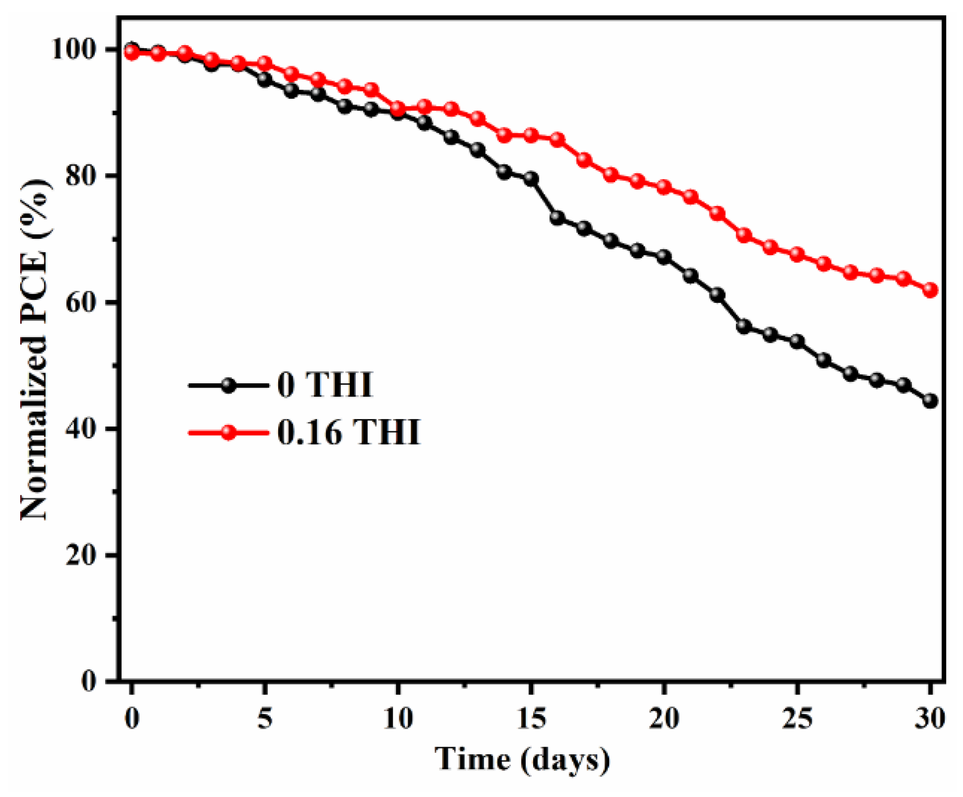
In addition to improving efficiency, device stability is also critical in achieving commercialization. The 30-day storage stability of PSCs without encapsulation was checked by storing them in a N2-filled glove box (with the content of both water and O2 being less than 1 ppm) and tested daily. The normalized PCEs as a function of time were recorded, as shown in Figure 5. The J−V curves of the PSCs after being stored for 1 day and 30 days are shown in Figure S4. After 30 days of storage, the PCE of the 0.16-THI-added device was maintained at 61.9% of its initial value, while it dropped to 44.3% for the control device. Obviously, the device based on THI-doped perovskite was more stable than the control device.
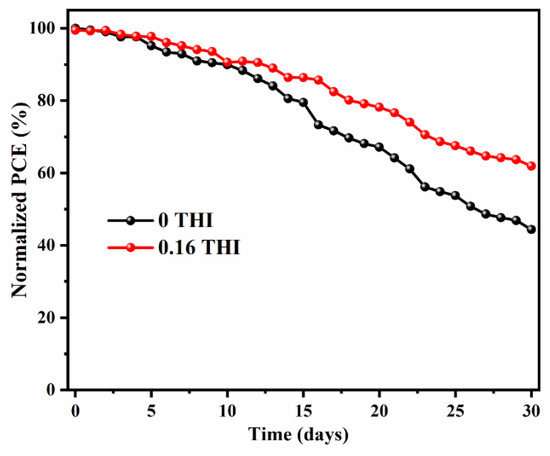
Figure 5.
Thirty-day storage stability of PSCs without encapsulation by storing in N2-filled glove box.
3. Discussion
XPS spectra demonstrated the interaction between THI and Pb2+, from which, it can be speculated that Lewis base–acid adducts were formed because of the strong Lewis base property of THI and Lewis acid property of Pb2+. The formation of Lewis base–acid adducts may slow down the perovskite crystal growth, beneficial to the formation of large grains [13]. The passivation of defects was also confirmed by the calculated defect density values from J−V of the electron-only device and EU values. The lowered defect density in perovskite films elevated the carrier mobility, which was inspected using Mottley–Gurney’s law from the J−V of electron-only device.
The improved film quality of perovskite with increased crystallinity, reduced defect density and elevated carrier mobility boosted its light absorbance and improved the extraction efficiency of electrons. Therefore, the VOC, JSC and FF of PSCs were all improved, leading to the great enhancement in PCE.
4. Materials and Methods
4.1. Materials
ITO substrate, PbI2 (99.99%), Pb(Ac)2 (99.99%), MAI (99.5%) and PCBM (99.5%) were purchased from Xi’an Polymer Light Technology Corp, Xi’an, China. BCP (99%) was purchased from Borun New Material Technology Corp, Ningbo, China. NiOx nanoparticles were synthesized in our lab according to the reference [36]. NiCl2·6H2O was purchased from MACKLIN, Shanghai, China. DMF (99.8%), chlorobenzene and DMSO were purchased from Sigma Aldrich, St. Louis, MO, USA. THI was purchased from J&K Scientific, Beijing, China. Ag (99.99%) was purchased from China New Metal, Beijing, China. SnO2 (15% in H2O colloidal dispersion) was purchased from Alfa Aesar, Thermo Fisher Scientific, Heysham, UK. All materials were used as received without further purification.
By co-dissolving MAI, PbI2 and Pb(Ac)2 powder in DMF with a molar ratio of 2.2:0.4:0.6, the perovskite precursor solution with a concentration of 1 mol/L was prepared. The addition of THI was performed by doping it in the perovskite precursor solution with weight ratios of 0.08 wt%, 0.16 wt% and 0.32 wt%, which was stirred for at least 6 h in a nitrogen-filled glove box before use. The PCBM solution was prepared by dissolving it in chlorobenzene with a concentration of 20 mg/mL. NiOx was ultrasonically dispersed in deionized water at a concentration of 20 mg mL−1 and filtered with a 0.45 µL water-based filter before using.
4.2. Device Fabrication
The device structure of PSC was composed of ITO/NiOx (20 nm)/MAPbI3 (260 nm)/PCBM (70 nm)/BCP (5 nm)/Ag (100 nm). Before use, ITO substrates were ultrasonically cleaned in sequence with detergent solution, deionized water, acetone and ethanol, taking 15 min for each step. After cleaning, the substrates were dried at 60 °C for 30 min in a bake oven. Then, O3 plasma surface treatment was applied for 4 min to remove the chemical residues on the surface of the ITO and facilitate the deposition of NiOx thin film. The NiOx solution was spin-coated on ITO at 2500 rpm for 30 s and then annealed at 130 °C for 10 min under atmospheric conditions. Following this, the ITO/NiOx samples were transferred to a nitrogen-filled glove box (with the content of both water and O2 being less than 1 ppm). The perovskite precursor solution was spin-coated at 4000 rpm for 30 s and then annealed on a hot plate at 100 °C for 15 min to form perovskite thin films. After that, the PCBM solution was spin-coated on top of the perovskite layer with a speed of 1200 rpm for 30 s and then thermal annealed on a hot plate at 100 °C for 2 min. Finally, a 5 nm thick BCP layer and a 100 nm thick Ag layer were sequentially thermally deposited under a pressure higher than 4 × 10⁻⁴ Pa. The active area defined by electrode masks was 0.09 cm2.
For the fabrication of electron-only devices with structures of ITO/SnO2/MAPbI3/ PCBM/Ag, SnO2 film was fabricated by spin-coating the SnO2 H2O colloidal dispersion on precleaned ITO at 3000 rpm for 30 s and then thermally annealing it at 150 °C for 30 min. Following this, MAPbI3, PCBM and Ag films were deposited using the above-mentioned processes.
4.3. Measurement and Characterization
XRD patterns of the perovskite films were obtained by using a Bruker D8 ADV ANCE X-ray diffractometer (Bruker Corp, Berlin, Germany) under the operation conditions of 40 kV and 40 mA. The absorption spectra were measured using a UV-visible spectrophotometer (UV3600, Shimadzu, Kyoto, Japan). The morphologies of perovskite films were observed via field emission scanning electron microscopy (FESEM, S4800 microscope, Hitachi Ltd., Tokyo, Japan). The steady-state PL was measured using an FLSP920 spectrometer (Edinburgh Instruments Ltd., Livingston, UK). X-ray photoelectron spectroscopy (XPS) was studied using a PHI Quantera SXM (ULVAC-PHI Inc., Tokyo, Japan). The current density–voltage (J−V) curves of the devices were measured using a Keithley 2400 Source Meter under an illumination of 1 sun (100 mW/cm2 AM 1.5 G, generated by a solar simulator Oriel Sol3A, Newport Corp., Irvine, CA, USA), which was calibrated with a standard Si photodiode. Incident photon-to-current efficiency (IPCE) data were collected by using a QTest Station1000 (Crowntch, Inc., Macungie, PA, USA). The electrochemical impedance spectrum (EIS) was tested using an electrochemical workstation (Zahner, Germany) under dark conditions.
Perovskite films for XRD, SEM, UV, PL and XPS tests were all prepared by spin-coating the perovskite precursor solution on ITO substrates with a concentration of 1 mol/L at 4000 rpm for 30 s. Then, the films were thermally annealed on a hot plate at 100 °C for 15 min. The films thicknesses were about 260 nm.
5. Conclusions
THI was introduced as an additive to the perovskite precursor solution. XPS spectra of Pb 4f in perovskite films verified the interaction between THI and uncoordinated Pb2+, which effectively reduced the defect density in perovskite film. Moreover, the crystallinity and grain size of perovskite films were significantly enhanced, leading to increased light absorbance, inhibited non-radiative recombination and enhanced charge carrier extraction. The doping concentration of THI was optimized in consideration of the performance of PSCs. With 0.16 wt% THI in the perovskite precursor solution, the PCE of PSCs increased from 16.49% to 18.97%. The storage stability of PSCs was also improved.
Supplementary Materials
The following supporting information can be downloaded at: https://www.mdpi.com/article/10.3390/molecules28134976/s1, Figure S1: The molecule structure of THI; Figure S2: The device configuration of PSCs. The films thicknesses were also included; Figure S3: PCE statistic of PSCs based on pristine (0 THI) and 0.16 THI perovskite film, 20 devices for each kind of device; Figure S4: J−V curves of the PSCs after being stored for one day and 30 days: (a) 0.16 THI-PSC and (b) control device.
Author Contributions
Methodology, W.H. and L.Z.; software, W.H. and L.Z.; validation, J.Y. and B.C.; formal analysis, L.Z.; investigation, W.H. and L.Z.; resources, W.Z.; data curation, Q.N.; writing—original draft preparation, W.H.; writing—review and editing, Q.N.; supervision, Q.N.; project administration, Q.N.; funding acquisition, R.X. and Y.M. All authors have read and agreed to the published version of the manuscript.
Funding
This research was funded by the National Natural Science Foundation of China (Grant Numbers: 61874058, 51861145301) and the Natural Science Foundation of NUPTSF (Grant Numbers: NY215077, NY215022).
Institutional Review Board Statement
Not applicable.
Informed Consent Statement
Not applicable.
Data Availability Statement
Data sharing not applicable.
Acknowledgments
The authors extend their appreciation to the National Natural Science Foundation of China (Grant Numbers: 61874058, 51861145301) and the Natural Science Foundation of NUPTSF (Grant Numbers: NY215077, NY215022) for funding this work.
Conflicts of Interest
The authors declare no conflict of interest.
Sample Availability
Not applicable.
References
- Lu, Q.; Yang, Z.; Meng, X.; Yue, Y.; Ahmad, M.A.; Zhang, W.; Zhang, S.; Zhang, Y.; Liu, Z.; Chen, W. A Review on Encapsulation Technology from Organic Light Emitting Diodes to Organic and Perovskite Solar Cells. Adv. Funct. Mater. 2021, 31, 2100151. [Google Scholar] [CrossRef]
- Zhang, Y.; Ma, Y.; Wang, Y.; Zhang, X.; Zuo, C.; Shen, L.; Ding, L. Lead-Free Perovskite Photodetectors: Progress, Challenges, and Opportunities. Adv. Mater. 2021, 33, e2006691. [Google Scholar] [CrossRef] [PubMed]
- Murugan, P.; Hu, T.; Hu, X.; Chen, Y. Advancements in organic small molecule hole-transporting materials for perovskite solar cells: Past and future. J. Mater. Chem. A 2022, 10, 5044–5081. [Google Scholar] [CrossRef]
- Zhuang, J.; Wang, J.; Yan, F. Review on Chemical Stability of Lead Halide Perovskite Solar Cells. Nano-Micro Lett. 2023, 15, 84. [Google Scholar] [CrossRef] [PubMed]
- Yi, F.X.; Guo, Q.Y.; Zheng, D.D.; Zhuang, R.; Zhang, J.S.; Tang, Q.W.; Duan, J.L. Multifunctional Polymer Capping Frameworks Enable High-Efficiency and Stable All-Inorganic Perovskite Solar Cells. ACS Appl. Energy Mater. 2022, 5, 6432–6441. [Google Scholar] [CrossRef]
- Guo, P.F.; Liu, C.; Li, X.L.; Chen, Z.G.; Zhu, H.F.; Zhu, L.G.; Zhang, X.H.; Zhao, W.H.; Jia, N.; Ye, Q.; et al. Laser Manufactured Nano-MXenes with Tailored Halogen Terminations Enable Interfacial Ionic Stabilization of High Performance Perovskite Solar Cells. Adv. Energy Mater. 2022, 12, 2202395. [Google Scholar] [CrossRef]
- Wu, T.; Qin, Z.; Wang, Y.; Wu, Y.; Chen, W.; Zhang, S.; Cai, M.; Dai, S.; Zhang, J.; Liu, J.; et al. The Main Progress of Perovskite Solar Cells in 2020–2021. Nano-Micro Lett. 2021, 13, 152. [Google Scholar] [CrossRef]
- Wu, T.H.; Cui, D.Y.; Liu, X.; Meng, X.Y.; Wang, Y.B.; Noda, T.; Segawa, H.; Yang, X.D.; Zhang, Y.Q.; Han, L.Y. Efficient and Stable Tin Perovskite Solar Cells Enabled by Graded Heterostructure of Light-Absorbing Layer. Solar Rrl 2020, 4, 2000240. [Google Scholar] [CrossRef]
- Ren, G.; Han, W.; Deng, Y.; Wu, W.; Li, Z.; Guo, J.; Bao, H.; Liu, C.; Guo, W. Strategies of modifying spiro-OMeTAD materials for perovskite solar cells: A review. J. Mater. Chem. A 2021, 9, 4589–4625. [Google Scholar] [CrossRef]
- Xin, D.; Tie, S.; Yuan, R.; Zheng, X.; Zhu, J.; Zhang, W.H. Defect Passivation in Hybrid Perovskite Solar Cells by Tailoring the Electron Density Distribution in Passivation Molecules. ACS Appl. Mater. Interfaces 2019, 11, 44233–44240. [Google Scholar] [CrossRef]
- Wu, T.; Li, X.; Qi, Y.; Zhang, Y.; Han, L. Defect Passivation for Perovskite Solar Cells: From Molecule Design to Device Performance. ChemSusChem 2021, 14, 4354–4376. [Google Scholar] [CrossRef] [PubMed]
- Zhou, J.; Yin, X.; Dong, Z.; Ali, A.; Song, Z.; Shrestha, N.; Bista, S.S.; Bao, Q.; Ellingson, R.J.; Yan, Y.; et al. Dithieno[3,2-b:2′,3′-d]pyrrole Cored p-Type Semiconductors Enabling 20% Efficiency Dopant-Free Perovskite Solar Cells. Angew. Chem. 2019, 58, 13717–13721. [Google Scholar] [CrossRef]
- Wang, Y.; Yang, Y.; Han, D.-W.; Yang, Q.-F.; Yuan, Q.; Li, H.-Y.; Yang, Y.; Zhou, D.-Y.; Feng, L. Amphoteric imidazole doping induced large-grained perovskite with reduced defect density for high performance inverted solar cells. Sol. Energy Mater. Sol. Cells 2020, 212, 110553. [Google Scholar] [CrossRef]
- Jia, J.B.; Shi, B.B.; Dong, J.; Jiang, Z.; Guo, S.B.; Wu, J.H.; Cao, B.Q. 4-Iodo-1H-imidazole dramatically improves the open-circuit voltages of perovskite solar cells to 1.2 V. New J. Chem. 2023, 47, 9913–9922. [Google Scholar] [CrossRef]
- Salado, M.; Jodlowski, A.D.; Roldan-Carmona, C.; de Miguel, G.; Kazim, S.; Nazeeruddin, M.K.; Ahmad, S. Surface passivation of perovskite layers using heterocyclic halides: Improved photovoltaic properties and intrinsic stability. Nano Energy 2018, 50, 220–228. [Google Scholar] [CrossRef]
- Chen, J.; Zhao, X.; Kim, S.G.; Park, N.G. Multifunctional Chemical Linker Imidazoleacetic Acid Hydrochloride for 21% Efficient and Stable Planar Perovskite Solar Cells. Adv. Mater. 2019, 31, e1902902. [Google Scholar] [CrossRef] [PubMed]
- Yang, D.; Zhou, X.; Yang, R.; Yang, Z.; Yu, W.; Wang, X.; Li, C.; Liu, S.; Chang, R.P.H. Surface optimization to eliminate hysteresis for record efficiency planar perovskite solar cells. Energy Environ. Sci. 2016, 9, 3071–3078. [Google Scholar] [CrossRef]
- Gao, Z.W.; Wang, Y.; Liu, H.; Sun, J.Y.; Kim, J.; Li, Y.; Xu, B.M.; Choy, W.C.H. Tailoring the Interface in FAPbI(3) Planar Perovskite Solar Cells by Imidazole-Graphene-Quantum-Dots. Adv. Funct. Mater. 2021, 31, 2101438. [Google Scholar] [CrossRef]
- Fei, C.; Guo, L.; Li, B.; Zhang, R.; Fu, H.; Tian, J.; Cao, G. Controlled growth of textured perovskite films towards high performance solar cells. Nano Energy 2016, 27, 17–26. [Google Scholar] [CrossRef]
- Liu, B.; Wang, S.; Ma, Z.; Ma, J.; Wang, C. High-Performance Perovskite Solar Cells with Large Grain-Size obtained by the synergy of urea and dimethyl sulfoxide. Appl. Surf. Sci. 2018, 467–468, 708–714. [Google Scholar] [CrossRef]
- Mehdizadeh-Rad, H.; Singh, J. Influence of Urbach Energy, Temperature, and Longitudinal Position in the Active Layer on Carrier Diffusion Length in Perovskite Solar Cells. Chemphyschem 2019, 20, 2712–2717. [Google Scholar] [CrossRef]
- Liu, F.; Ding, C.; Zhang, Y.S.; Ripolles, T.; Kamisaka, T.; Toyoda, T.; Hayase, S.; Minemoto, T.; Yoshino, K.; Dai, S.; et al. Colloidal Synthesis of Air-Stable Alloyed CsSn1-xPbxI3 Perovskite Nanocrystals for Use in Solar Cells. J. Am. Chem. Soc. 2017, 139, 16708–16719. [Google Scholar] [CrossRef]
- Wang, H.; Zou, W.; Ouyang, Y.; Luo, H.; Liu, X.; Li, H.; Lei, Y.; Ni, Y.; Fu, Y.; Zheng, D. Inducing crystal-oriented growth while inhibiting grain boundary migration with multifunctional ionic liquid for high-efficiency perovskite solar cells. J. Alloys Compd. 2022, 929, 167051. [Google Scholar] [CrossRef]
- Zheng, F.; Wen, X.; Bu, T.; Chen, S.; Yang, J.; Chen, W.; Huang, F.; Cheng, Y.; Jia, B. Slow Response of Carrier Dynamics in Perovskite Interface upon Illumination. ACS Appl. Mater. Interfaces 2018, 10, 31452–31461. [Google Scholar] [CrossRef]
- Choudhury, B.; Borah, B.; Choudhury, A. Extending Photocatalytic Activity of TiO2 Nanoparticles to Visible Region of Illumination by Doping of Cerium. Photochem. Photobiol. 2012, 88, 257–264. [Google Scholar] [CrossRef]
- Chen, J.; Seulgi, K.; Park, N.-G. FA0.88Cs0.12PbI3−x(PF6)x Interlayer Formed by Ion Exchange Reaction between Perovskite and Hole Transporting Layer for Improving Photovoltaic Performance and Stability. Adv. Mater. 2018, 30, 1801948. [Google Scholar] [CrossRef]
- Dong, Q.; Fang, Y.; Shao, Y.; Mulligan, P.; Qiu, J.; Cao, L.; Huang, J. Electron-hole diffusion lengths > 175 m in solution-grown CH3NH3PbI3 single crystals. Science 2015, 347, 967–970. [Google Scholar] [CrossRef]
- Bube, R. Trap Density Determination by Space-Charge-Limited Currents. J. Appl. Phys. 1962, 33, 1733–1737. [Google Scholar] [CrossRef]
- Jiang, Q.; Tong, J.; Xian, Y.; Kerner, R.A.; Dunfield, S.P.; Xiao, C.; Scheidt, R.A.; Kuciauskas, D.; Wang, X.; Hautzinger, M.P.; et al. Surface reaction for efficient and stable inverted perovskite solar cells. Nature 2022, 611, 278–283. [Google Scholar] [CrossRef]
- Kranthiraja, K.; Parashar, M.; Mehta, R.K.; Aryal, S.; Temsal, M.; Kaul, A.B. Stability and degradation in triple cation and methyl ammonium lead iodide perovskite solar cells mediated via Au and Ag electrodes. Sci. Rep. 2022, 12, 18574. [Google Scholar] [CrossRef] [PubMed]
- Emelianov, N.A.; Ozerova, V.V.; Zhidkov, I.S.; Korchagin, D.V.; Shilov, G.V.; Litvinov, A.L.; Kurmaev, E.Z.; Frolova, L.A.; Aldoshin, S.M.; Troshin, P.A. Nanoscale Visualization of Photodegradation Dynamics of MAPbI3 Perovskite Films. J. Phys. Chem. Lett. 2022, 13, 2744–2749. [Google Scholar] [CrossRef] [PubMed]
- Zhidkov, I.; Yu, M.-H.; Kukharenko, A.; Han, P.-C.; Cholakh, S.; Yu, W.-Y.; Wu, K.C.W.; Chueh, C.-C.; Kurmaev, E. The Stability of Hybrid Perovskites with UiO-66 Metal–Organic Framework Additives with Heat, Light, and Humidity. Nanomaterials 2022, 12, 4349. [Google Scholar] [CrossRef] [PubMed]
- Zhou, C.; Xu, X.; Liu, Z.; Sun, Z.; Chen, Z.; Chen, X.; Chen, L.; Fang, X.; Zhang, J.; Yang, Y.M.; et al. Bifunctional Hole-Transport Materials with Modification and Passivation Effect for High-Performance Inverted Perovskite Solar Cells. ACS Appl. Mater. Interfaces 2023, 15, 22752–22761. [Google Scholar] [CrossRef]
- Zhou, R.; Liu, X.; Li, H.; Peng, X.; Gong, X.; Ouyang, Y.; Luo, H.; Fu, Y.; Peng, Y. Multifunctional Passivation Strategy of Cationic and Anionic Defects for Efficient and Stable Perovskite Solar Cells. ACS Appl. Energy Mater. 2022, 5, 5928–5936. [Google Scholar] [CrossRef]
- Li, Y.; Ye, J.-J.; Medjahed, A.; Aldakov, D.; Pouget, S.; Djurado, E.; Xu, L.; Reiss, P. High Fill Factor and Reduced Hysteresis Perovskite Solar Cells Using Small-Molecule-Engineered Nickel Oxide as the Hole Transport Layer. ACS Appl. Energy Mater. 2023, 6, 1555–1564. [Google Scholar]
- Wang, J.; Galagan, Y.; von Hauff, E. Quantifying electrochemical losses in perovskite solar cells. J. Mater. Chem. C 2023, 11, 2911–2920. [Google Scholar] [CrossRef]
Disclaimer/Publisher’s Note: The statements, opinions and data contained in all publications are solely those of the individual author(s) and contributor(s) and not of MDPI and/or the editor(s). MDPI and/or the editor(s) disclaim responsibility for any injury to people or property resulting from any ideas, methods, instructions or products referred to in the content. |
© 2023 by the authors. Licensee MDPI, Basel, Switzerland. This article is an open access article distributed under the terms and conditions of the Creative Commons Attribution (CC BY) license (https://creativecommons.org/licenses/by/4.0/).

