
A Review on Cs-Based Pb-Free Double Halide Perovskites: From Theoretical and Experimental Studies to Doping and Applications


Abstract
1. Introduction
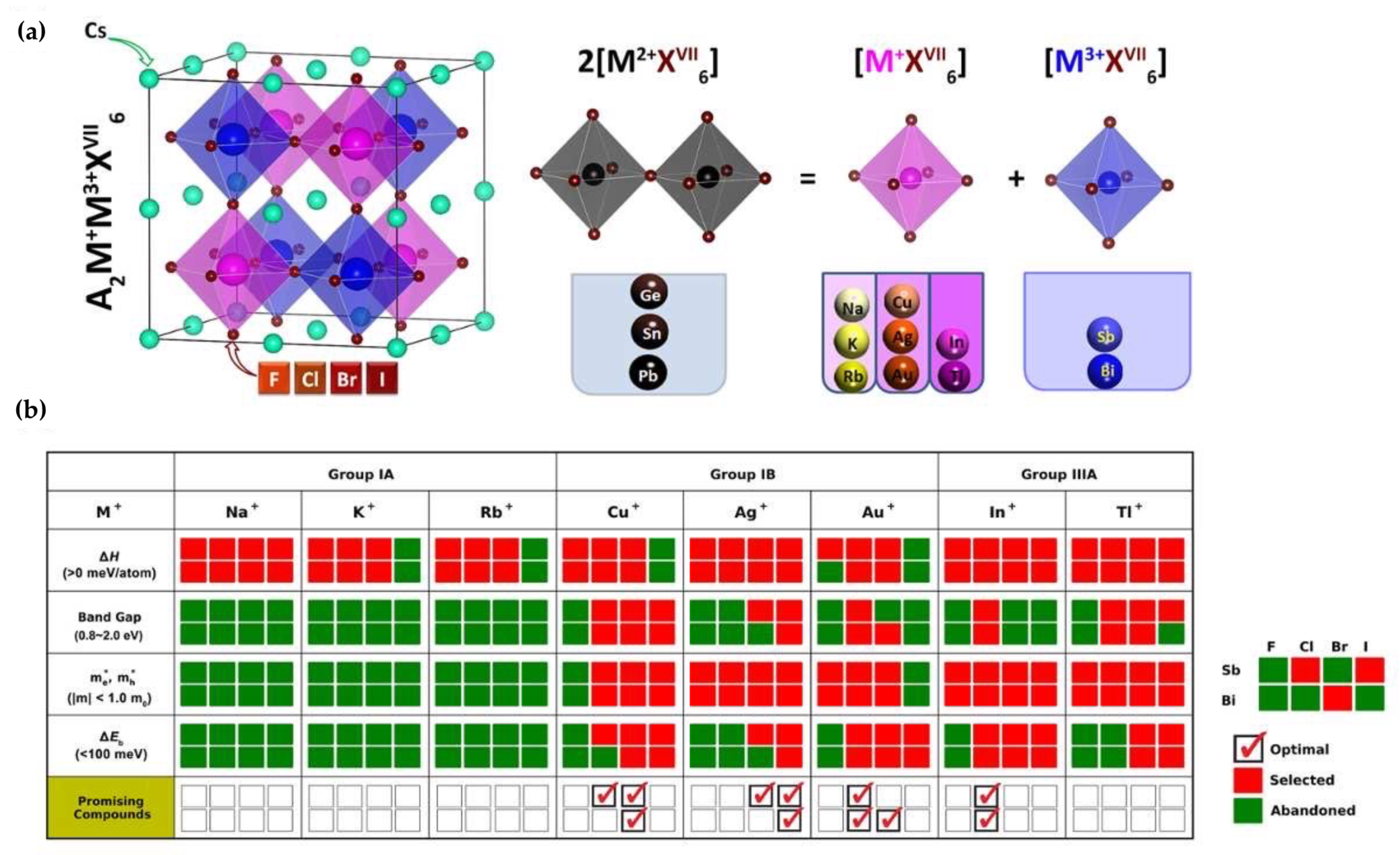
2. Double Halide Perovskites
2.1. Cs/Bi3+-Based Double Halide Perovskites
2.1.1. Cs2M+Bi3+X6: Theoretical Studies
2.1.2. Cs2M+Bi3+X6: Experimental Studies
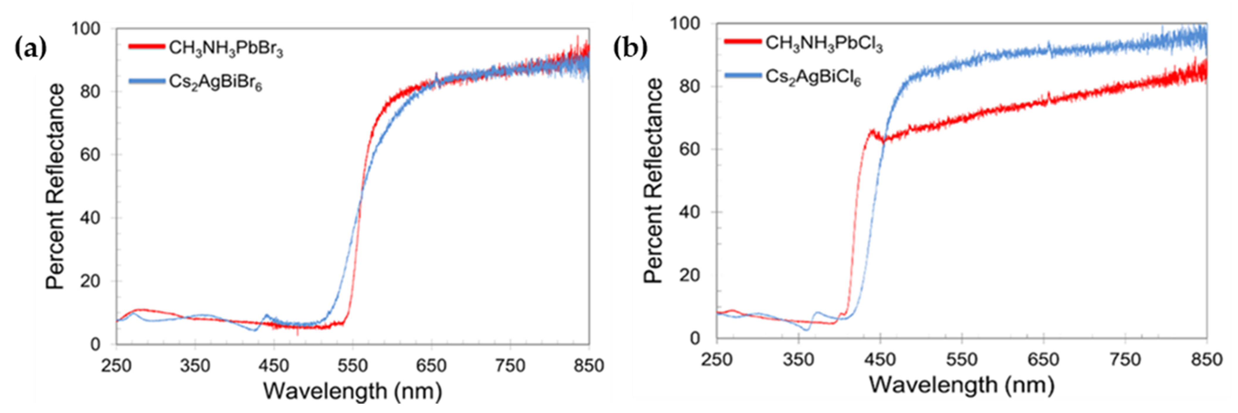
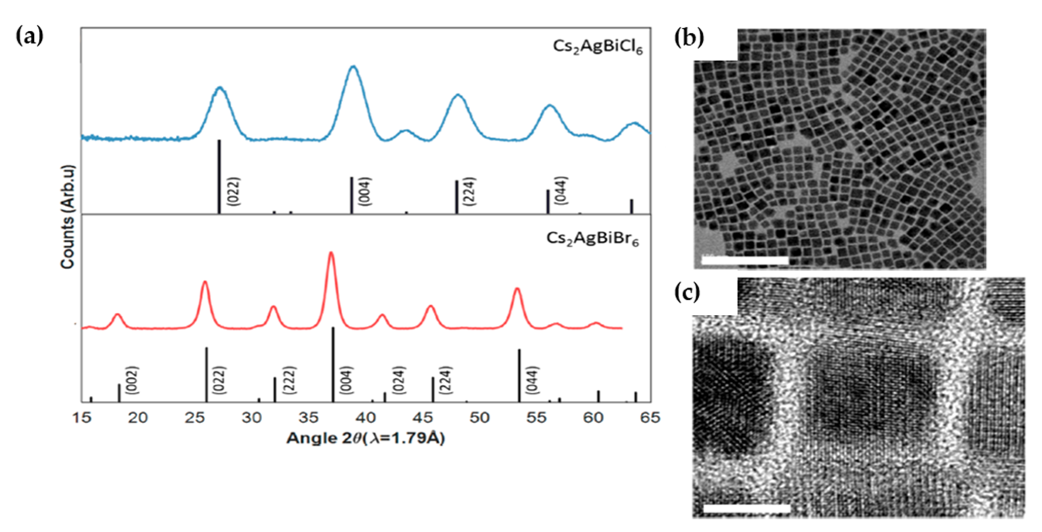
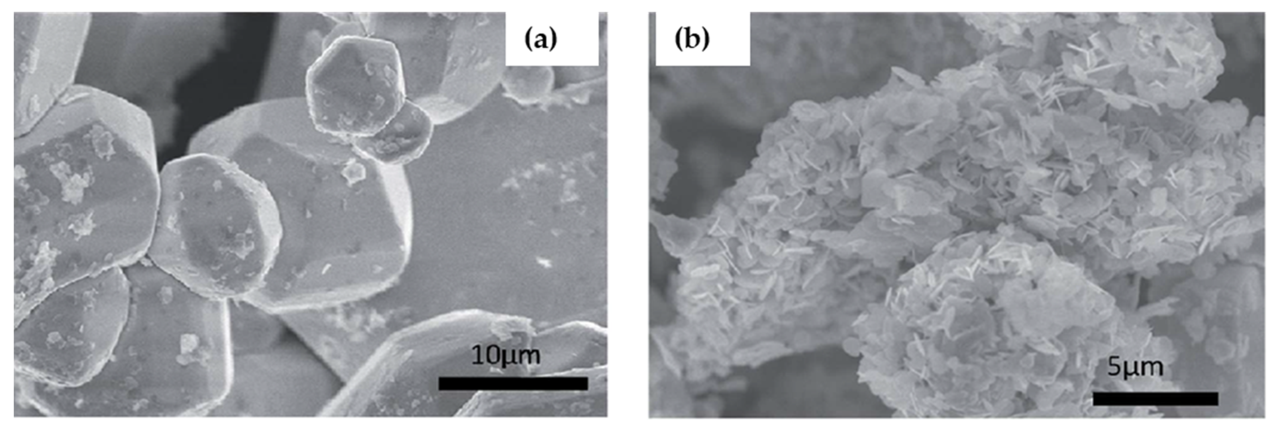
- Cs2M+Bi3+X6: Single-Crystals, Polycrystalline and Nanocrystals-Based Perovskites
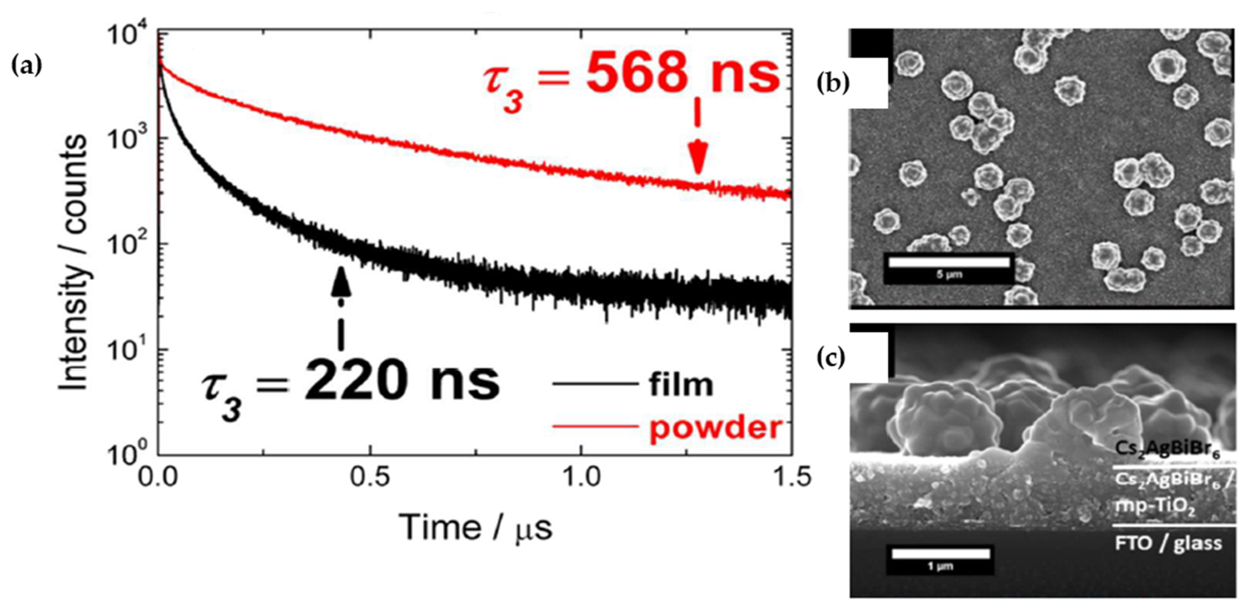
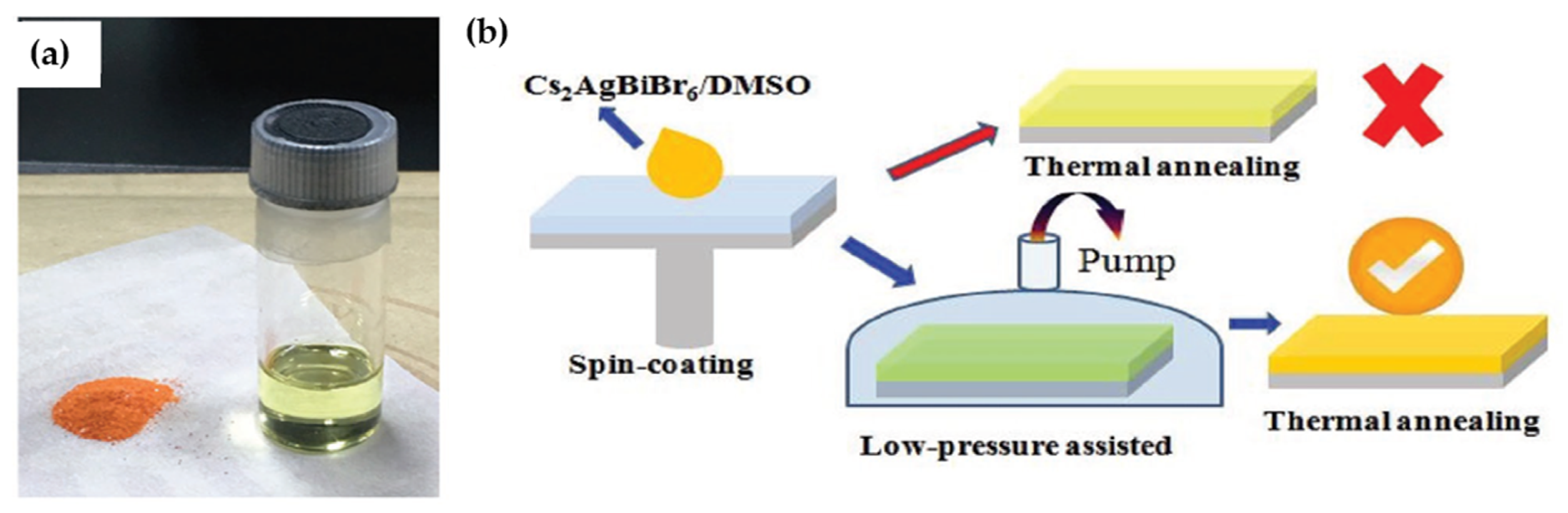
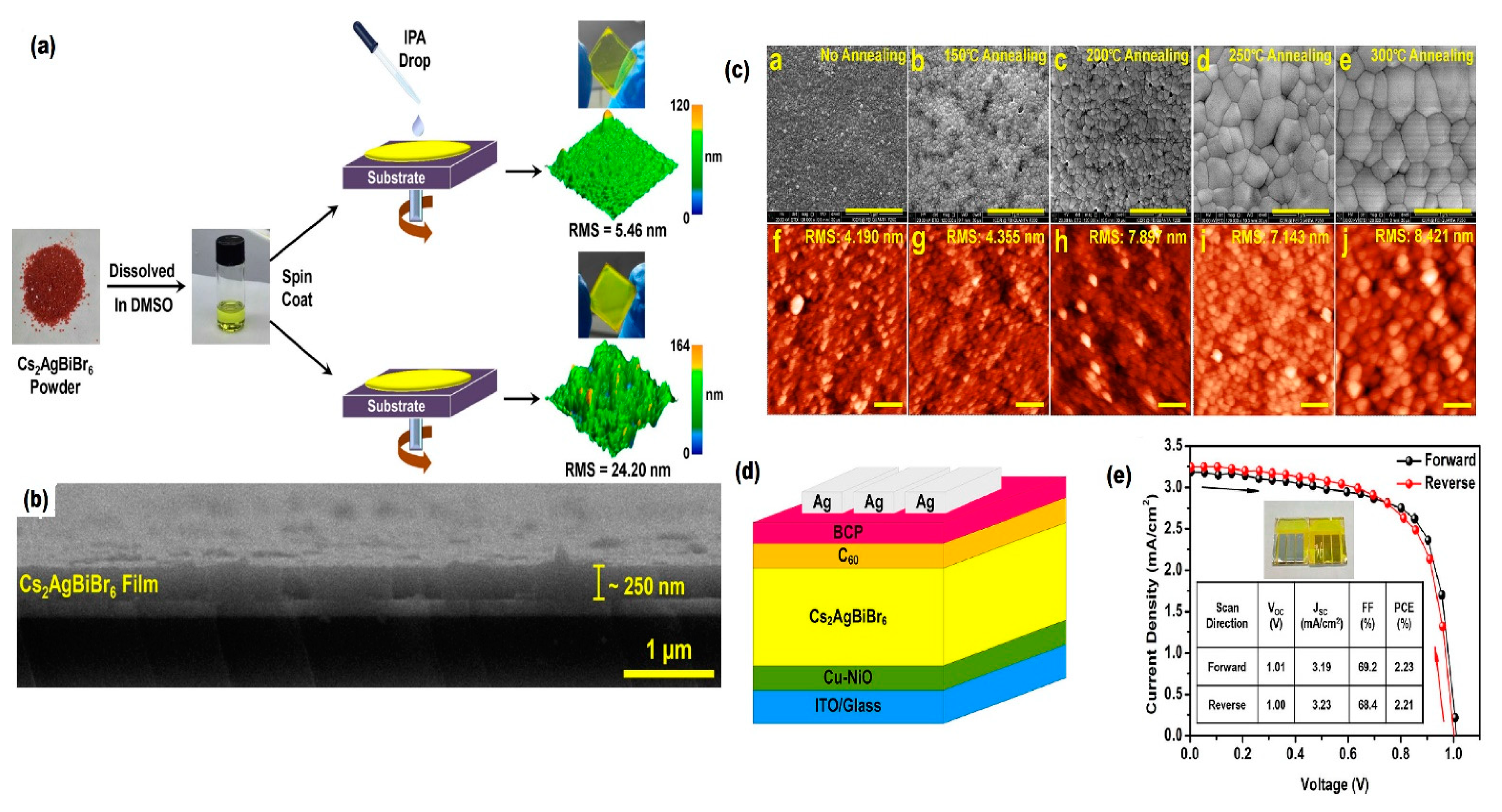
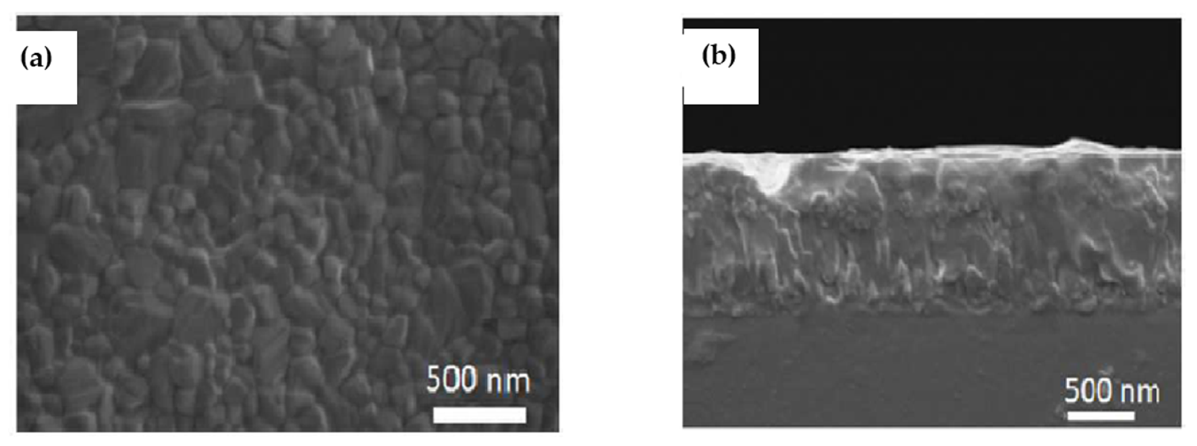
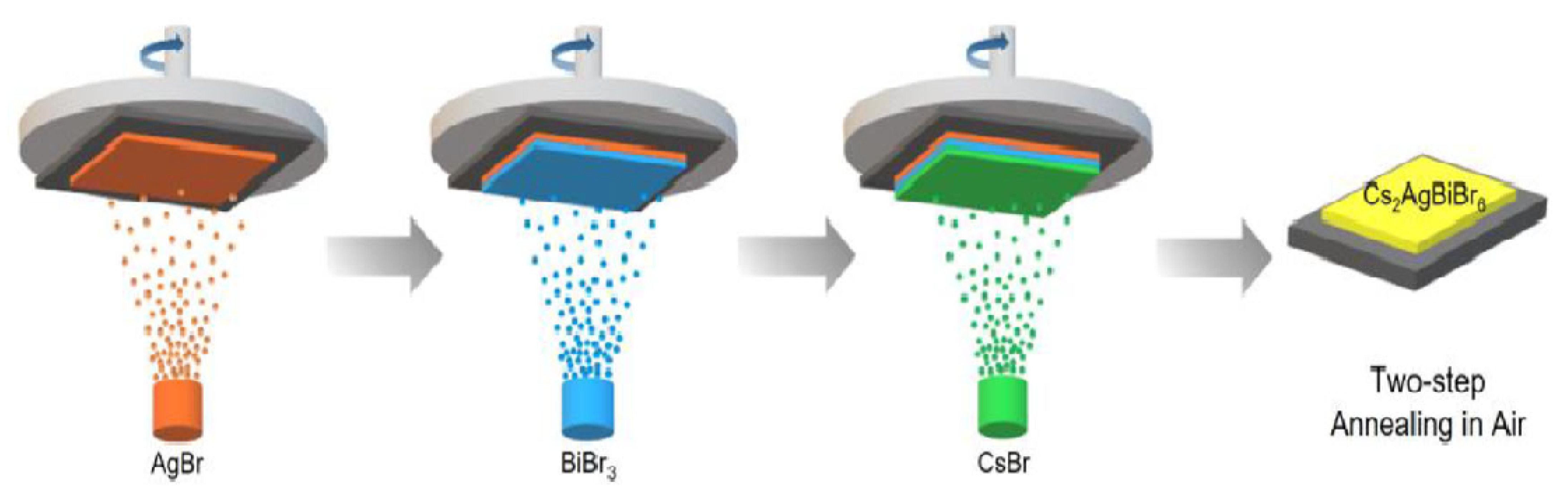
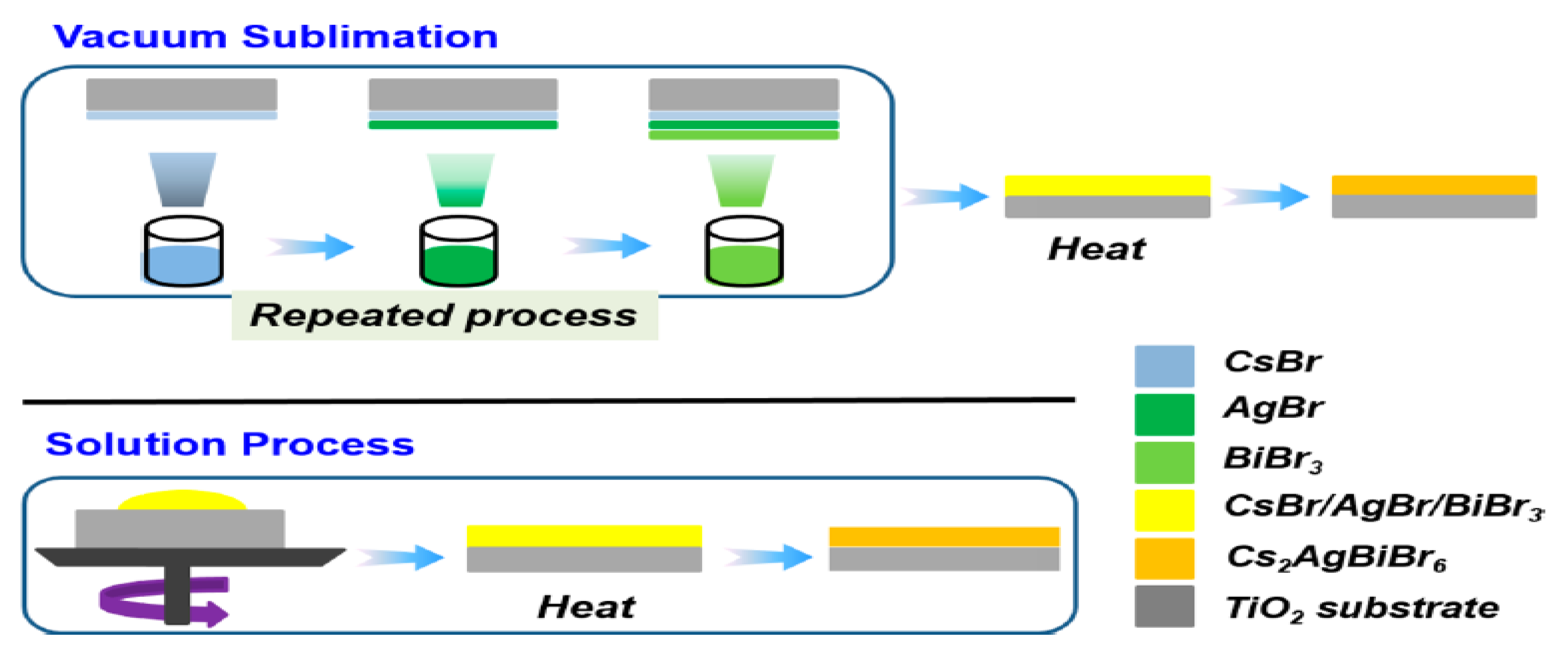
- Cs2M+Bi3+X6: Film-Based Perovskites
2.1.3. Cs2M+Bi3+X6: Doping
2.1.4. Cs2M+Bi3+X6: Applications
- Photovoltaic Applications
- Non-Photovoltaic Applications
2.2. Cs/In3+-Based Double Halide Perovskites
2.2.1. Cs2M+In3+X6: Theoretical Results
2.2.2. Cs2M+In3+X6: Experimental Results
- Cs2M+In3+X6: Single-Crystals, Polycrystalline and Nanocrystals-Based Perovskites
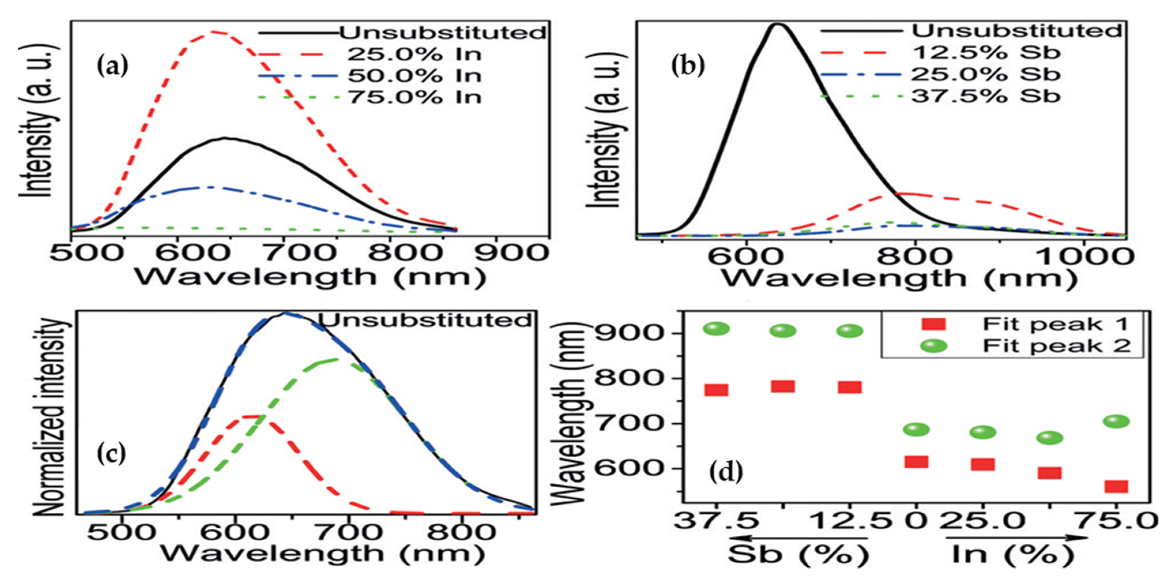
2.2.3. Cs2M+In3+X6: Doping
2.2.4. Cs2M+In3+X6: Applications
- Non-Photovoltaic Applications
2.3. Cs/Sb3+-Based Double Halide Perovskite
2.3.1. Cs2M+Sb3+X6: Theoretical Results
2.3.2. Cs2M+Sb3+X6: Experimental Results
- Cs2M+Sb3+X6: Single-Crystals, Polycrystalline and Nanocrystals-Based Perovskites
2.3.3. Cs2M+Sb3+X6: Doping
2.3.4. Cs2M+Sb3+X6: Applications
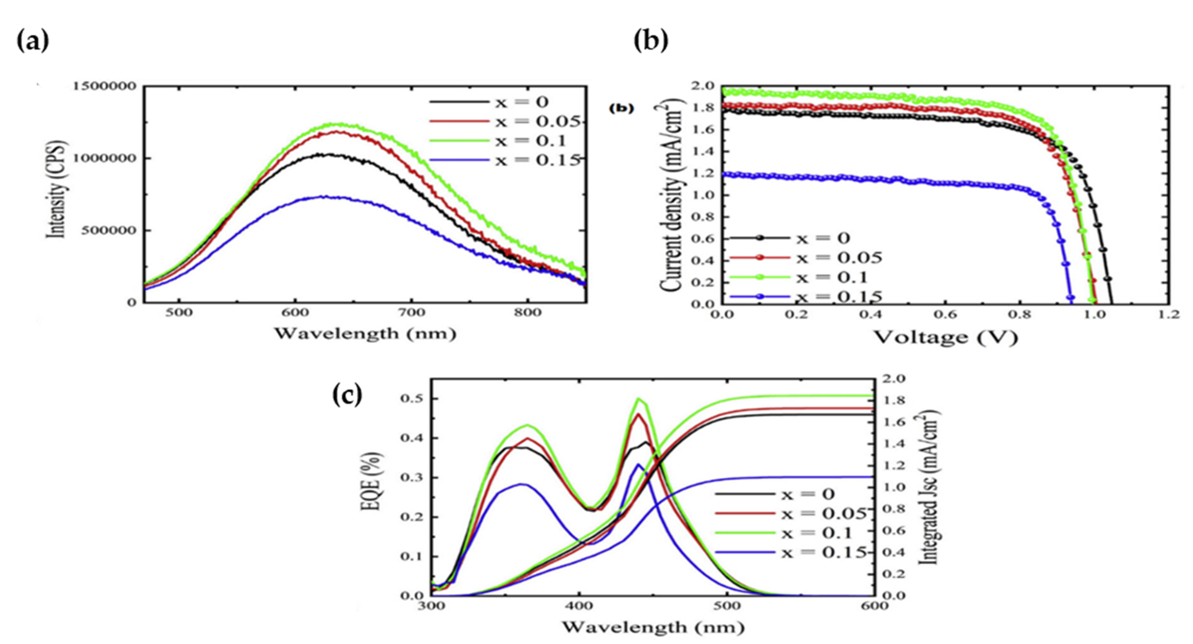
- Photovoltaic Applications
2.4. Cs-Based Vacancy-Ordered Double Halide Perovskites
2.4.1. Cs2M4+X6: Theoretical Results
2.4.2. Cs2M4+X6: Experimental Results
- Cs2M4+X6: Single-Crystals, Polycrystalline and Nanocrystals-Based Perovskites
- Cs2M4+X6: Film-Based
2.4.3. Cs2M4+X6: Doping
2.4.4. Cs2M4+X6: Applications
- Photovoltaic applications
3. Conclusions and Perspective
Author Contributions
Funding
Institutional Review Board Statement
Informed Consent Statement
Data Availability Statement
Acknowledgments
Conflicts of Interest
References
- Kojima, A.; Teshima, K.; Shirai, Y.; Miyasaka, T. Organometal halide perovskites as visible-light sensitizers for photovoltaic cells. J. Am. Chem. Soc. 2009, 131, 6050–6051. [Google Scholar] [CrossRef] [PubMed]
- Kim, H.-S.; Lee, C.-R.; Im, J.-H.; Lee, K.-B.; Moehl, T.; Marchioro, A.; Moon, S.-J.; Humphry-Baker, R.; Yum, J.-H.; Moser, J.E. Lead iodide perovskite sensitized all-solid-state submicron thin film mesoscopic solar cell with efficiency exceeding 9%. Sci. Rep. 2012, 2, 591. [Google Scholar] [CrossRef] [PubMed]
- Park, N.G. Research direction toward scalable, stable, and high efficiency perovskite solar cells. Adv. Energy Mater. 2020, 10, 1903106. [Google Scholar] [CrossRef]
- Seok, S.I.; Grätzel, M.; Park, N.G. Methodologies toward highly efficient perovskite solar cells. Small 2018, 14, 1704177. [Google Scholar] [CrossRef]
- Chu, L.; Ahmad, W.; Liu, W.; Yang, J.; Zhang, R.; Sun, Y.; Yang, J.; Li, X.A. Lead-Free Halide Double Perovskite Materials: A New Superstar Toward Green and Stable Optoelectronic Applications. Nano-Micro Lett. 2019, 11, 16. [Google Scholar] [CrossRef]
- Giustino, F.; Snaith, H.J. Toward lead-free perovskite solar cells. ACS Energy Lett. 2016, 1, 1233–1240. [Google Scholar] [CrossRef]
- De Wolf, S.; Holovsky, J.; Moon, S.-J.; Löper, P.; Niesen, B.; Ledinsky, M.; Haug, F.-J.; Yum, J.-H.; Ballif, C. Organometallic halide perovskites: Sharp optical absorption edge and its relation to photovoltaic performance. J. Phys. Chem. Lett. 2014, 5, 1035–1039. [Google Scholar] [CrossRef]
- Chin, X.Y.; Cortecchia, D.; Yin, J.; Bruno, A.; Soci, C. Lead iodide perovskite light-emitting field-effect transistor. Nat. Commun. 2015, 6, 7383. [Google Scholar] [CrossRef]
- Huang, H.; Raith, J.; Kershaw, S.V.; Kalytchuk, S.; Tomanec, O.; Jing, L.; Susha, A.S.; Zboril, R.; Rogach, A.L. Growth mechanism of strongly emitting CH3NH3PbBr3 perovskite nanocrystals with a tunable bandgap. Nat. Commun. 2017, 8, 1–8. [Google Scholar] [CrossRef]
- Tan, Z.-K.; Moghaddam, R.S.; Lai, M.L.; Docampo, P.; Higler, R.; Deschler, F.; Price, M.; Sadhanala, A.; Pazos, L.M.; Credgington, D. Bright light-emitting diodes based on organometal halide perovskite. Nat. Nanotechnol. 2014, 9, 687–692. [Google Scholar] [CrossRef]
- Zhu, H.; Fu, Y.; Meng, F.; Wu, X.; Gong, Z.; Ding, Q.; Gustafsson, M.V.; Trinh, M.T.; Jin, S.; Zhu, X. Lead halide perovskite nanowire lasers with low lasing thresholds and high quality factors. Nat. Mater. 2015, 14, 636–642. [Google Scholar] [CrossRef] [PubMed]
- Ramasamy, P.; Lim, D.-H.; Kim, B.; Lee, S.-H.; Lee, M.-S.; Lee, J.-S. All-inorganic cesium lead halide perovskite nanocrystals for photodetector applications. Chem. Commun. 2016, 52, 2067–2070. [Google Scholar] [CrossRef]
- Hu, X.; Zhang, X.; Liang, L.; Bao, J.; Li, S.; Yang, W.; Xie, Y. High-performance flexible broadband photodetector based on organolead halide perovskite. Adv. Funct. Mater. 2014, 24, 7373–7380. [Google Scholar] [CrossRef]
- Wei, H.; Fang, Y.; Mulligan, P.; Chuirazzi, W.; Fang, H.-H.; Wang, C.; Ecker, B.R.; Gao, Y.; Loi, M.A.; Cao, L. Sensitive X-ray detectors made of methylammonium lead tribromide perovskite single crystals. Nat. Photonics 2016, 10, 333. [Google Scholar] [CrossRef]
- Hoefler, S.F.; Trimmel, G.; Rath, T. Progress on lead-free metal halide perovskites for photovoltaic applications: A review. Mon. Chem. Chem. Mon. 2017, 148, 795–826. [Google Scholar] [CrossRef]
- Babayigit, A.; Ethirajan, A.; Muller, M.; Conings, B. Toxicity of organometal halide perovskite solar cells. Nat. Mater. 2016, 15, 247. [Google Scholar] [CrossRef]
- Fu, H. Review of lead-free halide perovskites as light-absorbers for photovoltaic applications: From materials to solar cells. Sol. Energy Mater. Sol. Cells 2019, 193, 107–132. [Google Scholar] [CrossRef]
- Jaishankar, M.; Tseten, T.; Anbalagan, N.; Mathew, B.B.; Beeregowda, K.N. Toxicity, mechanism and health effects of some heavy metals. Interdiscip. Toxicol. 2014, 7, 60–72. [Google Scholar] [CrossRef]
- Tchounwou, P.B.; Yedjou, C.G.; Patlolla, A.K.; Sutton, D.J. Heavy metal toxicity and the environment. In Molecular, Clinical and Environmental Toxicology; Springer: Berlin/Heidelberg, Germany, 2012; pp. 133–164. [Google Scholar]
- Abate, A. Perovskite solar cells go lead free. Joule 2017, 1, 659–664. [Google Scholar] [CrossRef]
- Aristidou, N.; Sanchez-Molina, I.; Chotchuangchutchaval, T.; Brown, M.; Martinez, L.; Rath, T.; Haque, S.A. The role of oxygen in the degradation of methylammonium lead trihalide perovskite photoactive layers. Angew. Chem. Int. Ed. 2015, 54, 8208–8212. [Google Scholar] [CrossRef]
- Hailegnaw, B.; Kirmayer, S.; Edri, E.; Hodes, G.; Cahen, D. Rain on methylammonium lead iodide based perovskites: Possible environmental effects of perovskite solar cells. J. Phys. Chem. Lett. 2015, 6, 1543–1547. [Google Scholar] [CrossRef]
- Habisreutinger, S.N.; McMeekin, D.P.; Snaith, H.J.; Nicholas, R.J. Research Update: Strategies for improving the stability of perovskite solar cells. APL Mater. 2016, 4, 091503. [Google Scholar] [CrossRef]
- Heo, J.; Im, S.; Noh, J.; Madal, T.; Lim, C.; Chang, J.; Lee, Y.; Kim, H.; Sarkar, A.; Nazeeruddin, M.K. Efficient inorganic-organic hybrid heterojunction solar cells containing perovskite compound and polymeric hole conductors. Nano Lett. 2013, 13, 1764. [Google Scholar] [CrossRef]
- Wang, Z.; Shi, Z.; Li, T.; Chen, Y.; Huang, W. Stability of perovskite solar cells: A prospective on the substitution of the A cation and X anion. Angew. Chem. Int. Ed. 2017, 56, 1190–1212. [Google Scholar] [CrossRef] [PubMed]
- Emami, S.; Andrade, L.; Mendes, A. Recent progress in long-term stability of perovskite solar cells. U. Porto J. Eng. 2015, 1, 52–62. [Google Scholar] [CrossRef]
- Liu, W.; Lin, Q.; Li, H.; Wu, K.; Robel, I.; Pietryga, J.M.; Klimov, V.I. Mn2+-doped lead halide perovskite nanocrystals with dual-color emission controlled by halide content. J. Am. Chem. Soc. 2016, 138, 14954–14961. [Google Scholar] [CrossRef]
- Abdi-Jalebi, M.; Dar, M.I.; Sadhanala, A.; Senanayak, S.P.; Franckevičius, M.; Arora, N.; Hu, Y.; Nazeeruddin, M.K.; Zakeeruddin, S.M.; Grätzel, M. Impact of monovalent cation halide additives on the structural and optoelectronic properties of CH3NH3PbI3 perovskite. Adv. Energy Mater. 2016, 6, 1502472. [Google Scholar] [CrossRef]
- Shahbazi, S.; Tsai, C.-M.; Narra, S.; Wang, C.-Y.; Shiu, H.-S.; Afshar, S.; Taghavinia, N.; Diau, E.W.-G. Ag doping of organometal lead halide perovskites: Morphology modification and p-type character. J. Phys. Chem. C 2017, 121, 3673–3679. [Google Scholar] [CrossRef]
- Yang, Y.; Zou, X.; Pei, Y.; Bai, X.; Jin, W.; Chen, D. Effect of doping of NaI monovalent cation halide on the structural, morphological, optical and optoelectronic properties of MAPbI3 perovskite. J. Mater. Sci. Mater. Electron. 2018, 29, 205–210. [Google Scholar] [CrossRef]
- Wu, M.-C.; Chen, W.-C.; Chan, S.-H.; Su, W.-F. The effect of strontium and barium doping on perovskite-structured energy materials for photovoltaic applications. Appl. Surf. Sci. 2018, 429, 9–15. [Google Scholar] [CrossRef]
- Zhao, W.; Yang, D.; Yang, Z.; Liu, S.F. Zn-doping for reduced hysteresis and improved performance of methylammonium lead iodide perovskite hybrid solar cells. Mater. Today Energy 2017, 5, 205–213. [Google Scholar] [CrossRef]
- Zhang, Z.; Ren, L.; Yan, H.; Guo, S.; Wang, S.; Wang, M.; Jin, K. Bandgap narrowing in Bi-doped CH3NH3PbCl3 perovskite single crystals and thin films. J. Phys. Chem. C 2017, 121, 17436–17441. [Google Scholar] [CrossRef]
- Oku, T.; Ohishi, Y.; Suzuki, A. Effects of antimony addition to perovskite-type CH3NH3PbI3 photovoltaic devices. Chem. Lett. 2016, 45, 134–136. [Google Scholar] [CrossRef]
- Grancini, G.; Roldán-Carmona, C.; Zimmermann, I.; Mosconi, E.; Lee, X.; Martineau, D.; Narbey, S.; Oswald, F.; De Angelis, F.; Graetzel, M. One-Year stable perovskite solar cells by 2D/3D interface engineering. Nat. Commun. 2017, 8, 1–8. [Google Scholar] [CrossRef]
- Li, H.; Luo, T.; Zhang, S.; Sun, Z.; He, X.; Zhang, W.; Chang, H. Two-dimensional metal-halide perovskite-based optoelectronics: Synthesis, structure, properties and applications. Energy Environ. Mater. 2021, 4, 46–64. [Google Scholar] [CrossRef]
- Qian, L.; Sun, Y.; Sun, M.; Fang, Z.; Li, L.; Xie, D.; Li, C.; Ding, L. 2D perovskite microsheets for high-performance photodetectors. J. Mater. Chem. C 2019, 7, 5353–5358. [Google Scholar] [CrossRef]
- Tang, S.; Huang, S.; Wilson, G.J.; Ho-Baillie, A. Progress and Opportunities for Cs Incorporated Perovskite Photovoltaics. Trends Chem. 2020, 2, 638–653. [Google Scholar] [CrossRef]
- Umari, P.; Mosconi, E.; De Angelis, F. Relativistic GW calculations on CH3NH3PbI3 and CH3NH3SnI3 perovskites for solar cell applications. Sci. Rep. 2014, 4, 4467. [Google Scholar] [CrossRef] [PubMed]
- Yin, W.J.; Shi, T.; Yan, Y. Unique properties of halide perovskites as possible origins of the superior solar cell performance. Adv. Mater. 2014, 26, 4653–4658. [Google Scholar] [CrossRef]
- Zhang, Q.; Hao, F.; Li, J.; Zhou, Y.; Wei, Y.; Lin, H. Perovskite solar cells: Must lead be replaced—And can it be done? Sci. Technol. Adv. Mater. 2018, 19, 425–442. [Google Scholar] [CrossRef]
- Stoumpos, C.C.; Malliakas, C.D.; Kanatzidis, M.G. Semiconducting tin and lead iodide perovskites with organic cations: Phase transitions, high mobilities, and near-infrared photoluminescent properties. Inorg. Chem. 2013, 52, 9019–9038. [Google Scholar] [CrossRef]
- Wu, B.; Zhou, Y.; Xing, G.; Xu, Q.; Garces, H.F.; Solanki, A.; Goh, T.W.; Padture, N.P.; Sum, T.C. Long minority-carrier diffusion length and low surface-recombination velocity in inorganic lead-free CsSnI3 perovskite crystal for solar cells. Adv. Funct. Mater. 2017, 27, 1604818. [Google Scholar] [CrossRef]
- Noel, N.K.; Stranks, S.D.; Abate, A.; Wehrenfennig, C.; Guarnera, S.; Haghighirad, A.-A.; Sadhanala, A.; Eperon, G.E.; Pathak, S.K.; Johnston, M.B. Lead-free organic–inorganic tin halide perovskites for photovoltaic applications. Energy Environ. Sci. 2014, 7, 3061–3068. [Google Scholar] [CrossRef]
- Hebig, J.-C.; Kühn, I.; Flohre, J.; Kirchartz, T. Optoelectronic properties of (CH3NH3) 3Sb2I9 thin films for photovoltaic applications. ACS Energy Lett. 2016, 1, 309–314. [Google Scholar] [CrossRef]
- Pazoki, M.; Edvinsson, T. Metal replacement in perovskite solar cell materials: Chemical bonding effects and optoelectronic properties. Sustain. Energy Fuels 2018, 2, 1430–1445. [Google Scholar] [CrossRef]
- Singh, T.; Kulkarni, A.; Ikegami, M.; Miyasaka, T. Effect of electron transporting layer on bismuth-based lead-free perovskite (CH3NH3)3Bi2I9 for photovoltaic applications. ACS Appl. Mater. Interfaces 2016, 8, 14542–14547. [Google Scholar] [CrossRef] [PubMed]
- Slavney, A.H.; Hu, T.; Lindenberg, A.M.; Karunadasa, H.I. A bismuth-halide double perovskite with long carrier recombination lifetime for photovoltaic applications. J. Am. Chem. Soc. 2016, 138, 2138–2141. [Google Scholar] [CrossRef] [PubMed]
- McClure, E.T.; Ball, M.R.; Windl, W.; Woodward, P.M. Cs2AgBiX6 (X= Br, Cl): New visible light absorbing, lead-free halide perovskite semiconductors. Chem. Mater. 2016, 28, 1348–1354. [Google Scholar] [CrossRef]
- Volonakis, G.; Filip, M.R.; Haghighirad, A.A.; Sakai, N.; Wenger, B.; Snaith, H.J.; Giustino, F. Lead-free halide double perovskites via heterovalent substitution of noble metals. J. Phys. Chem. Lett. 2016, 7, 1254–1259. [Google Scholar] [CrossRef]
- Xiao, Z.; Meng, W.; Wang, J.; Mitzi, D.B.; Yan, Y. Searching for promising new perovskite-based photovoltaic absorbers: The importance of electronic dimensionality. Mater. Horiz. 2017, 4, 206–216. [Google Scholar] [CrossRef]
- Kangsabanik, J.; Sugathan, V.; Yadav, A.; Yella, A.; Alam, A. Double perovskites overtaking the single perovskites: A set of new solar harvesting materials with much higher stability and efficiency. Phys. Rev. Mater. 2018, 2, 055401. [Google Scholar] [CrossRef]
- Meng, W.; Wang, X.; Xiao, Z.; Wang, J.; Mitzi, D.B.; Yan, Y. Parity-forbidden transitions and their impact on the optical absorption properties of lead-free metal halide perovskites and double perovskites. J. Phys. Chem. Lett. 2017, 8, 2999–3007. [Google Scholar] [CrossRef]
- Zhao, X.-G.; Yang, J.-H.; Fu, Y.; Yang, D.; Xu, Q.; Yu, L.; Wei, S.-H.; Zhang, L. Design of lead-free inorganic halide perovskites for solar cells via cation-transmutation. J. Am. Chem. Soc. 2017, 139, 2630–2638. [Google Scholar] [CrossRef]
- Mohan, R. Green bismuth. Nat. Chem. 2010, 2, 336. [Google Scholar] [CrossRef] [PubMed]
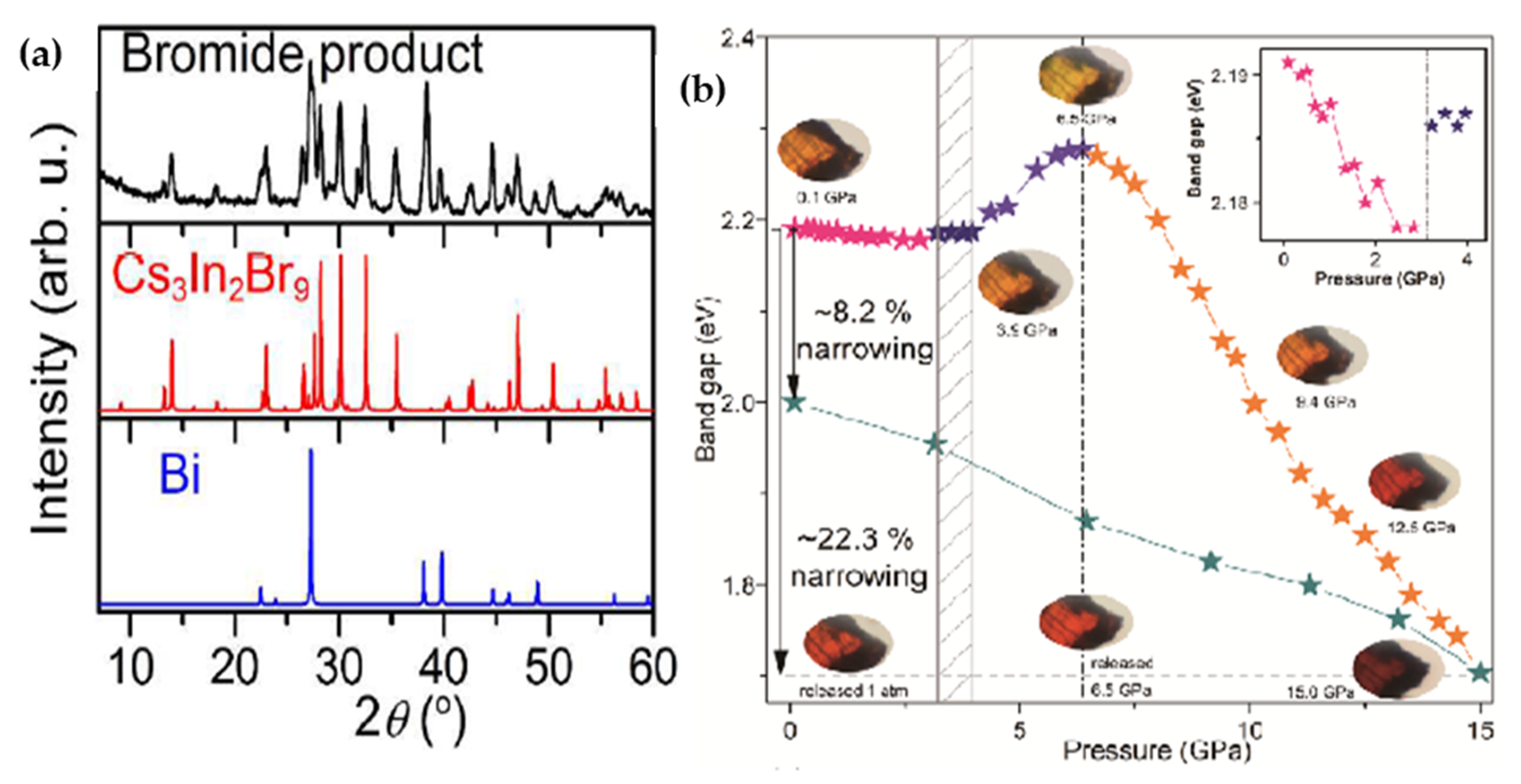
- Li, Q.; Wang, Y.; Pan, W.; Yang, W.; Zou, B.; Tang, J.; Quan, Z. High-Pressure Band-Gap Engineering in Lead-Free Cs2AgBiBr6 Double Perovskite. Angew. Chem. Int. Ed. 2017, 56, 15969–15973. [Google Scholar] [CrossRef] [PubMed]
- Filip, M.R.; Hillman, S.; Haghighirad, A.A.; Snaith, H.J.; Giustino, F. Band gaps of the lead-free halide double perovskites Cs2BiAgCl6 and Cs2BiAgBr6 from theory and experiment. J. Phys. Chem. Lett. 2016, 7, 2579–2585. [Google Scholar] [CrossRef] [PubMed]
- Yang, J.; Zhang, P.; Wei, S.-H. Band structure engineering of Cs2AgBiBr6 perovskite through order–disordered transition: A first-principle study. J. Phys. Chem. Lett. 2018, 9, 31–35. [Google Scholar] [CrossRef]
- Bekenstein, Y.; Dahl, J.C.; Huang, J.; Osowiecki, W.T.; Swabeck, J.K.; Chan, E.M.; Yang, P.; Alivisatos, A.P. The making and breaking of lead-free double perovskite nanocrystals of cesium silver-bismuth halide compositions. Nano Lett. 2018, 18, 3502–3508. [Google Scholar] [CrossRef]
- Hoye, R.L.; Eyre, L.; Wei, F.; Brivio, F.; Sadhanala, A.; Sun, S.; Li, W.; Zhang, K.H.; MacManus-Driscoll, J.L.; Bristowe, P.D. Fundamental carrier lifetime exceeding 1 µs in Cs2AgBiBr6 double perovskite. Adv. Mater. Interfaces 2018, 5, 1800464. [Google Scholar] [CrossRef]
- Zelewski, S.; Urban, J.; Surrente, A.; Maude, D.; Kuc, A.; Schade, L.; Johnson, R.; Dollmann, M.; Nayak, P.; Snaith, H. Revealing the nature of photoluminescence emission in the metal-halide double perovskite Cs2AgBiBr6. J. Mater. Chem. C 2019, 7, 8350–8356. [Google Scholar] [CrossRef]
- Wei, F.; Deng, Z.; Sun, S.; Hartono, N.T.P.; Seng, H.L.; Buonassisi, T.; Bristowe, P.D.; Cheetham, A.K. Enhanced visible light absorption for lead-free double perovskite Cs2AgSbBr6. Chem. Commun. 2019, 55, 3721–3724. [Google Scholar] [CrossRef]
- García-Espejo, G.; Rodríguez-Padrón, D.; Luque, R.; Camacho, L.; de Miguel, G. Mechanochemical synthesis of three double perovskites: Cs2AgBiBr6,(CH3NH3)2TlBiBr6 and Cs2AgSbBr6. Nanoscale 2019, 11, 16650–16657. [Google Scholar] [CrossRef]
- Wang, B.; Yang, L.; Dall’Agnese, C.; Jena, A.K.; Sasaki, S.-I.; Miyasaka, T.; Tamiaki, H.; Wang, X.-F. Photoactive Zn-chlorophyll hole transporter-sensitized lead-free Cs2AgBiBr6 perovskite solar cells. Sol. RRL 2020, 4, 2000166. [Google Scholar] [CrossRef]
- Yang, X.; Chen, Y.; Liu, P.; Xiang, H.; Wang, W.; Ran, R.; Zhou, W.; Shao, Z. Simultaneous Power Conversion Efficiency and Stability Enhancement of Cs2AgBiBr6 Lead-Free Inorganic Perovskite Solar Cell through Adopting a Multifunctional Dye Interlayer. Adv. Funct. Mater. 2020, 30, 2001557. [Google Scholar] [CrossRef]
- Wang, B.; Li, N.; Yang, L.; Dall’Agnese, C.; Jena, A.K.; Sasaki, S.-I.; Miyasaka, T.; Tamiaki, H.; Wang, X.-F. Chlorophyll Derivative-Sensitized TiO2 Electron Transport Layer for Record Efficiency of Cs2AgBiBr6 Double Perovskite Solar Cells. J. Am. Chem. Soc. 2021, 143, 2207–2211. [Google Scholar] [CrossRef]
- Xiao, Z.; Du, K.-Z.; Meng, W.; Wang, J.; Mitzi, D.B.; Yan, Y. Intrinsic instability of Cs2In(I)M(III)X6 (M = Bi, Sb; X = halogen) double perovskites: A combined density functional theory and experimental study. J. Am. Chem. Soc. 2017, 139, 6054–6057. [Google Scholar] [CrossRef]
- Lin, Y.-P.; Hu, S.; Xia, B.; Fan, K.-Q.; Gong, L.-K.; Kong, J.-T.; Huang, X.-Y.; Xiao, Z.; Du, K.-Z. Material Design and Optoelectronic Properties of Three-Dimensional Quadruple Perovskite Halides. J. Phys. Chem. Lett. 2019, 10, 5219–5225. [Google Scholar] [CrossRef]
- Xiao, Z.; Meng, W.; Wang, J.; Yan, Y. Thermodynamic Stability and Defect Chemistry of Bismuth-Based Lead-Free Double Perovskites. ChemSusChem 2016, 9, 2628–2633. [Google Scholar] [CrossRef] [PubMed]
- Dronskowski, R. In3Ti2Br9: Jahn-Teller Unstable Indium (i) and Antiferromagnetically Coupled Titanium (iii) Atoms. Chem. Eur. J. 1995, 1, 118–123. [Google Scholar] [CrossRef]
- Van den Berg, J.M. The crystal structure of the room temperature modification of indium chloride, InCl. Acta Crystallogr. 1966, 20, 905–910. [Google Scholar] [CrossRef]
- Li, B.; Bian, K.; Zhou, X.; Lu, P.; Liu, S.; Brener, I.; Sinclair, M.; Luk, T.; Schunk, H.; Alarid, L. Pressure compression of CdSe nanoparticles into luminescent nanowires. Sci. Adv. 2017, 3, e1602916. [Google Scholar] [CrossRef]
- Protesescu, L.; Yakunin, S.; Bodnarchuk, M.I.; Krieg, F.; Caputo, R.; Hendon, C.H.; Yang, R.X.; Walsh, A.; Kovalenko, M.V. Nanocrystals of cesium lead halide perovskites (CsPbX3, X= Cl, Br, and I): Novel optoelectronic materials showing bright emission with wide color gamut. Nano Lett. 2015, 15, 3692–3696. [Google Scholar] [CrossRef]
- Xu, K.; Lin, C.C.; Xie, X.; Meijerink, A. Efficient and stable luminescence from Mn2+ in core and core-isocrystalline shell CsPbCl3 perovskite nanocrystals. Chem. Mater. 2017, 29, 4265–4272. [Google Scholar] [CrossRef]
- Zhang, C.; Gao, L.; Teo, S.; Guo, Z.; Xu, Z.; Zhao, S.; Ma, T. Design of a novel and highly stable lead-free Cs2NaBiI6 double perovskite for photovoltaic application. Sustain. Energy Fuels 2018, 2, 2419–2428. [Google Scholar] [CrossRef]
- Pelant, I.; Valenta, J. Luminescence Spectroscopy of Semiconductors; Oxford University Press: Oxford, UK, 2012. [Google Scholar]
- Greul, E.; Petrus, M.L.; Binek, A.; Docampo, P.; Bein, T. Highly stable, phase pure Cs2AgBiBr6 double perovskite thin films for optoelectronic applications. J. Mater. Chem. A 2017, 5, 19972–19981. [Google Scholar] [CrossRef]
- Wu, C.; Zhang, Q.; Liu, Y.; Luo, W.; Guo, X.; Huang, Z.; Ting, H.; Sun, W.; Zhong, X.; Wei, S. The Dawn of Lead-Free Perovskite Solar Cell: Highly Stable Double Perovskite Cs2AgBiBr6 Film. Adv. Sci. 2018, 5, 1700759. [Google Scholar] [CrossRef]
- Ning, W.; Wang, F.; Wu, B.; Lu, J.; Yan, Z.; Liu, X.; Tao, Y.; Liu, J.M.; Huang, W.; Fahlman, M. Long Electron-Hole Diffusion Length in High-Quality Lead-Free Double Perovskite Films. Adv. Mater. 2018, 30, 1706246. [Google Scholar] [CrossRef]
- Pantaler, M.; Cho, K.T.; Queloz, V.I.; Garciȷa Benito, I.S.; Fettkenhauer, C.; Anusca, I.; Nazeeruddin, M.K.; Lupascu, D.C.; Grancini, G. Hysteresis-free lead-free double-perovskite solar cells by interface engineering. ACS Energy Lett. 2018, 3, 1781–1786. [Google Scholar] [CrossRef]
- Gao, W.; Ran, C.; Xi, J.; Jiao, B.; Zhang, W.; Wu, M.; Hou, X.; Wu, Z. High-Quality Cs2AgBiBr6 Double Perovskite Film for Lead-Free Inverted Planar Heterojunction Solar Cells with 2.2% Efficiency. ChemPhysChem 2018, 19, 1696–1700. [Google Scholar] [CrossRef]
- Wang, M.; Zeng, P.; Bai, S.; Gu, J.; Li, F.; Yang, Z.; Liu, M. High-Quality Sequential-Vapor-Deposited Cs2AgBiBr6 Thin Films for Lead-Free Perovskite Solar Cells. Sol. RRL 2018, 2, 1800217. [Google Scholar] [CrossRef]
- Igbari, F.; Wang, R.; Wang, Z.-K.; Ma, X.-J.; Wang, Q.; Wang, K.-L.; Zhang, Y.; Liao, L.-S.; Yang, Y. Composition stoichiometry of Cs2AgBiBr6 films for highly efficient lead-free perovskite solar cells. Nano Lett. 2019, 19, 2066–2073. [Google Scholar] [CrossRef]
- Zhang, Z.; Wu, C.; Wang, D.; Liu, G.; Zhang, Q.; Luo, W.; Qi, X.; Guo, X.; Zhang, Y.; Lao, Y. Improvement of Cs2AgBiBr6 double perovskite solar cell by rubidium doping. Org. Electron. 2019, 74, 204–210. [Google Scholar] [CrossRef]
- Dahl, J.C.; Osowiecki, W.T.; Cai, Y.; Swabeck, J.K.; Bekenstein, Y.; Asta, M.; Chan, E.M.; Alivisatos, A.P. Probing the stability and band gaps of Cs2AgInCl6 and Cs2AgSbCl6 lead-free double perovskite nanocrystals. Chem. Mater. 2019, 31, 3134–3143. [Google Scholar] [CrossRef]
- Qiu, X.; Cao, B.; Yuan, S.; Chen, X.; Qiu, Z.; Jiang, Y.; Ye, Q.; Wang, H.; Zeng, H.; Liu, J. From unstable CsSnI3 to air-stable Cs2SnI6: A lead-free perovskite solar cell light absorber with bandgap of 1.48 eV and high absorption coefficient. Sol. Energy Mater. Sol. Cells 2017, 159, 227–234. [Google Scholar] [CrossRef]
- Chen, M.; Ju, M.-G.; Carl, A.D.; Zong, Y.; Grimm, R.L.; Gu, J.; Zeng, X.C.; Zhou, Y.; Padture, N.P. Cesium titanium (IV) bromide thin films based stable lead-free perovskite solar cells. Joule 2018, 2, 558–570. [Google Scholar] [CrossRef]
- Arora, N.; Dar, M.I.; Hinderhofer, A.; Pellet, N.; Schreiber, F.; Zakeeruddin, S.M.; Grätzel, M. Perovskite solar cells with CuSCN hole extraction layers yield stabilized efficiencies greater than 20%. Science 2017, 358, 768–771. [Google Scholar] [CrossRef]
- Khalfin, S.; Bekenstein, Y. Advances in lead-free double perovskite nanocrystals, engineering band-gaps and enhancing stability through composition tunability. Nanoscale 2019, 11, 8665–8679. [Google Scholar] [CrossRef]
- Xu, L.; Yuan, S.; Zeng, H.; Song, J. A comprehensive review of doping in perovskite nanocrystals/quantum dots: Evolution of structure, electronics, optics and light-emitting diodes. Mater. Today Nano 2019, 100036. [Google Scholar] [CrossRef]
- Slavney, A.H.; Leppert, L.; Bartesaghi, D.; Gold-Parker, A.; Toney, M.F.; Savenije, T.J.; Neaton, J.B.; Karunadasa, H.I. Defect-induced band-edge reconstruction of a bismuth-halide double perovskite for visible-light absorption. J. Am. Chem. Soc. 2017, 139, 5015–5018. [Google Scholar] [CrossRef]
- Du, K.z.; Meng, W.; Wang, X.; Yan, Y.; Mitzi, D.B. Bandgap Engineering of Lead-Free Double Perovskite Cs2AgBiBr6 through Trivalent Metal Alloying. Angew. Chem. Int. Ed. 2017, 56, 8158–8162. [Google Scholar] [CrossRef]
- Yang, B.; Mao, X.; Hong, F.; Meng, W.; Tang, Y.; Xia, X.; Yang, S.; Deng, W.; Han, K. Lead-free direct band gap double-perovskite nanocrystals with bright dual-color emission. J. Am. Chem. Soc. 2018, 140, 17001–17006. [Google Scholar] [CrossRef]
- Majher, J.D.; Gray, M.B.; Strom, T.A.; Woodward, P.M. Cs2NaBiCl6: Mn2+—A New Orange-Red Halide Double Perovskite Phosphor. Chem. Mater. 2019, 31, 1738–1744. [Google Scholar] [CrossRef]
- Yao, M.M.; Wang, L.; Yao, J.S.; Wang, K.H.; Chen, C.; Zhu, B.S.; Yang, J.N.; Wang, J.J.; Xu, W.P.; Zhang, Q. Improving Lead-Free Double Perovskite Cs2NaBiCl6 Nanocrystal Optical Properties via Ion Doping. Adv. Opt. Mater. 2020, 8, 1901919. [Google Scholar] [CrossRef]
- Nag, A. Synthesis and luminescence of Mn-doped Cs2AgInCl6 double perovskites. Chem. Commun. 2018, 54, 5205–5208. [Google Scholar]
- Locardi, F.; Cirignano, M.; Baranov, D.; Dang, Z.; Prato, M.; Drago, F.; Ferretti, M.; Pinchetti, V.; Fanciulli, M.; Brovelli, S. Colloidal synthesis of double perovskite Cs2AgInCl6 and Mn-doped Cs2AgInCl6 nanocrystals. J. Am. Chem. Soc. 2018, 140, 12989–12995. [Google Scholar] [CrossRef]
- Hu, Q.; Niu, G.; Zheng, Z.; Li, S.; Zhang, Y.; Song, H.; Zhai, T.; Tang, J. Tunable Color Temperatures and Efficient White Emission from Cs2Ag1− xNaxIn1− yBiyCl6 Double Perovskite Nanocrystals. Small 2019, 15, 1903496. [Google Scholar] [CrossRef]
- Liu, Y.; Jing, Y.; Zhao, J.; Liu, Q.; Xia, Z. Design optimization of lead-free perovskite Cs2AgInCl6: Bi nanocrystals with 11.4% photoluminescence quantum yield. Chem. Mater. 2019, 31, 3333–3339. [Google Scholar] [CrossRef]
- Mahor, Y.; Mir, W.J.; Nag, A. Synthesis and near-infrared emission of Yb-doped Cs2AgInCl6 double perovskite microcrystals and nanocrystals. J. Phys. Chem. C 2019, 123, 15787–15793. [Google Scholar] [CrossRef]
- Gray, M.; Hariyani, S.; Strom, A.; Majher, J.; Brgoch, J.; Woodward, P. High-Efficiency Blue Photoluminescence in the Cs 2 NaInCl 6: Sb 3+ Double Perovskite Phosphor. J. Mater. Chem. C 2020, 8, 6797–6803. [Google Scholar] [CrossRef]
- Zeng, R.; Zhang, L.; Xue, Y.; Ke, B.; Zhao, Z.; Huang, D.; Wei, Q.; Zhou, W.; Zou, B. Highly Efficient Blue Emission from Self-Trapped Excitons in Stable Sb3+-Doped Cs2NaInCl6 Double Perovskites. J. Phys. Chem. Lett. 2020, 11, 2053–2061. [Google Scholar] [CrossRef]
- Karmakar, A.; Dodd, M.S.; Agnihotri, S.; Ravera, E.; Michaelis, V.K. Cu (II)-doped Cs2SbAgCl6 double perovskite: A lead-free, low-bandgap material. Chem. Mater. 2018, 30, 8280–8290. [Google Scholar] [CrossRef]
- Kshirsagar, A.S.; Nag, A. Synthesis and optical properties of colloidal Cs2AgSb1−xBixCl6 double perovskite nanocrystals. J. Chem. Phys. 2019, 151, 161101. [Google Scholar] [CrossRef]
- Yang, B.; Hong, F.; Chen, J.; Tang, Y.; Yang, L.; Sang, Y.; Xia, X.; Guo, J.; He, H.; Yang, S. Colloidal Synthesis and Charge-Carrier Dynamics of Cs2AgSb1− yBiyX6 (X: Br, Cl; 0 ≤ y ≤ 1) Double Perovskite Nanocrystals. Angew. Chem. 2019, 131, 2300–2305. [Google Scholar] [CrossRef]
- Maughan, A.E.; Ganose, A.M.; Almaker, M.A.; Scanlon, D.O.; Neilson, J.R. Tolerance factor and cooperative tilting effects in vacancy-ordered double perovskite halides. Chem. Mater. 2018, 30, 3909–3919. [Google Scholar] [CrossRef]
- Tan, Z.; Li, J.; Zhang, C.; Li, Z.; Hu, Q.; Xiao, Z.; Kamiya, T.; Hosono, H.; Niu, G.; Lifshitz, E. Highly Efficient Blue-Emitting Bi-Doped Cs2SnCl6 Perovskite Variant: Photoluminescence Induced by Impurity Doping. Adv. Funct. Mater. 2018, 28, 1801131. [Google Scholar] [CrossRef]
- Ma, X.X.; Li, Z.S. Influence of Sn/Ge Cation Exchange on Vacancy-Ordered Double Perovskite Cs2Sn(1−x)GexI6: A First-Principles Theoretical Study. Phys. Status Solidi (B) 2019, 256, 1800427. [Google Scholar] [CrossRef]
- Wang, F.; Bai, S.; Tress, W.; Hagfeldt, A.; Gao, F. Defects engineering for high-performance perovskite solar cells. NPJ Flex. Electron. 2018, 2, 1–14. [Google Scholar] [CrossRef]
- Volonakis, G.; Giustino, F. Surface properties of lead-free halide double perovskites: Possible visible-light photo-catalysts for water splitting. Appl. Phys. Lett. 2018, 112, 243901. [Google Scholar] [CrossRef]
- Pan, W.; Wu, H.; Luo, J.; Deng, Z.; Ge, C.; Chen, C.; Jiang, X.; Yin, W.-J.; Niu, G.; Zhu, L. Cs2AgBiBr6 single-crystal X-ray detectors with a low detection limit. Nat. Photonics 2017, 11, 726–732. [Google Scholar] [CrossRef]
- Yuan, W.; Niu, G.; Xian, Y.; Wu, H.; Wang, H.; Yin, H.; Liu, P.; Li, W.; Fan, J. In Situ Regulating the Order–Disorder Phase Transition in Cs2AgBiBr6 Single Crystal toward the Application in an X-ray Detector. Adv. Funct. Mater. 2019, 29, 1900234. [Google Scholar] [CrossRef]
- Li, H.; Shan, X.; Neu, J.N.; Geske, T.; Davis, M.; Mao, P.; Xiao, K.; Siegrist, T.; Yu, Z. Lead-free halide double perovskite-polymer composites for flexible X-ray imaging. J. Mater. Chem. C 2018, 6, 11961–11967. [Google Scholar] [CrossRef]
- Lei, L.-Z.; Shi, Z.-F.; Li, Y.; Ma, Z.-Z.; Zhang, F.; Xu, T.-T.; Tian, Y.-T.; Wu, D.; Li, X.-J.; Du, G.-T. High-efficiency and air-stable photodetectors based on lead-free double perovskite Cs2AgBiBr6 thin films. J. Mater. Chem. C 2018, 6, 7982–7988. [Google Scholar] [CrossRef]
- Wu, C.; Du, B.; Luo, W.; Liu, Y.; Li, T.; Wang, D.; Guo, X.; Ting, H.; Fang, Z.; Wang, S. Highly efficient and stable self-powered ultraviolet and deep-blue photodetector based on Cs2AgBiBr6/SnO2 heterojunction. Adv. Opt. Mater. 2018, 6, 1800811. [Google Scholar] [CrossRef]
- Zhou, L.; Xu, Y.F.; Chen, B.X.; Kuang, D.B.; Su, C.Y. Synthesis and Photocatalytic Application of Stable Lead-Free Cs2AgBiBr6 Perovskite Nanocrystals. Small 2018, 14, 1703762. [Google Scholar] [CrossRef]
- Zhang, Z.; Liang, Y.; Huang, H.; Liu, X.; Li, Q.; Chen, L.; Xu, D. Stable and Highly Efficient Photocatalysis with Lead-Free Double-Perovskite of Cs2AgBiBr6. Angew. Chem. Int. Ed. 2019, 58, 7263–7267. [Google Scholar] [CrossRef]
- Volonakis, G.; Haghighirad, A.A.; Milot, R.L.; Sio, W.H.; Filip, M.R.; Wenger, B.; Johnston, M.B.; Herz, L.M.; Snaith, H.J.; Giustino, F. Cs2InAgCl6: A new lead-free halide double perovskite with direct band gap. J. Phys. Chem. Lett. 2017, 8, 772–778. [Google Scholar] [CrossRef]
- Zhao, X.-G.; Yang, D.; Sun, Y.; Li, T.; Zhang, L.; Yu, L.; Zunger, A. Cu–In halide perovskite solar absorbers. J. Am. Chem. Soc. 2017, 139, 6718–6725. [Google Scholar] [CrossRef]
- Chirilă, A.; Buecheler, S.; Pianezzi, F.; Bloesch, P.; Gretener, C.; Uhl, A.R.; Fella, C.; Kranz, L.; Perrenoud, J.; Seyrling, S. Highly efficient Cu(In,Ga)Se2 solar cells grown on flexible polymer films. Nat. Mater. 2011, 10, 857–861. [Google Scholar] [CrossRef]
- Zhang, S.; Wei, S.-H.; Zunger, A.; Katayama-Yoshida, H. Defect physics of the CuInSe2 chalcopyrite semiconductor. Phys. Rev. B 1998, 57, 9642. [Google Scholar] [CrossRef]
- Persson, C.; Zunger, A. Anomalous Grain Boundary Physics in Polycrystalline CuInSe2: The Existence of a Hole Barrier. Phys. Rev. Lett. 2003, 91, 266401. [Google Scholar] [CrossRef]
- Xu, J.; Liu, J.-B.; Liu, B.-X.; Huang, B. Intrinsic defect physics in indium-based lead-free halide double perovskites. J. Phys. Chem. Lett. 2017, 8, 4391–4396. [Google Scholar] [CrossRef]
- Zhou, J.; Xia, Z.; Molokeev, M.S.; Zhang, X.; Peng, D.; Liu, Q. Composition design, optical gap and stability investigations of lead-free halide double perovskite Cs2AgInCl6. J. Mater. Chem. A 2017, 5, 15031–15037. [Google Scholar] [CrossRef]
- Tran, T.T.; Panella, J.R.; Chamorro, J.R.; Morey, J.R.; McQueen, T.M. Designing indirect-direct bandgap transitions in double perovskites. Mater. Horiz. 2017, 4, 688–693. [Google Scholar] [CrossRef]
- Wu, W.; Cong, W.-Y.; Guan, C.; Sun, H.; Yin, R.; Yu, G.; Lu, Y.-B. Investigation of the Mn dopant-enhanced photoluminescence performance of lead-free Cs2AgInCl6 double perovskite crystals. Phys. Chem. Chem. Phys. 2020, 22, 1815–1819. [Google Scholar] [CrossRef]
- Luo, J.; Li, S.; Wu, H.; Zhou, Y.; Li, Y.; Liu, J.; Li, J.; Li, K.; Yi, F.; Niu, G. Cs2AgInCl6 double perovskite single crystals: Parity forbidden transitions and their application for sensitive and fast UV photodetectors. ACS Photonics 2018, 5, 398–405. [Google Scholar] [CrossRef]
- Arfin, H.; Kaur, J.; Sheikh, T.; Chakraborty, S.; Nag, A. Bi3+-Er3+ and Bi3+-Yb3+ Codoped Cs2AgInCl6 Double Perovskite Near Infrared Emitters. Angew. Chem. Int. Ed. Engl. 2020, 59, 11307–11311. [Google Scholar] [CrossRef]
- Vargas, B.; Ramos, E.; Pérez-Gutiérrez, E.; Alonso, J.C.; Solis-Ibarra, D. A Direct Bandgap Copper–Antimony Halide Perovskite. J. Am. Chem. Soc. 2017, 139, 9116–9119. [Google Scholar] [CrossRef]
- Zhou, J.; Rong, X.; Molokeev, M.S.; Zhang, X.; Xia, Z. Exploring the transposition effects on the electronic and optical properties of Cs2AgSbCl6 via a combined computational-experimental approach. J. Mater. Chem. A 2018, 6, 2346–2352. [Google Scholar] [CrossRef]
- Filip, M.R.; Liu, X.; Miglio, A.; Hautier, G.; Giustino, F. Phase diagrams and stability of lead-free halide double perovskites Cs2BB′ X6: B= Sb and Bi, B′= Cu, Ag, and Au, and X= Cl, Br, and I. J. Phys. Chem. C 2018, 122, 158–170. [Google Scholar] [CrossRef]
- Deng, W.; Deng, Z.-Y.; He, J.; Wang, M.; Chen, Z.-X.; Wei, S.-H.; Feng, H.-J. Synthesis of Cs2AgSbCl6 and improved optoelectronic properties of Cs2AgSbCl6/TiO2 heterostructure driven by the interface effect for lead-free double perovskites solar cells. Appl. Phys. Lett. 2017, 111, 151602. [Google Scholar] [CrossRef]
- Kieslich, G.; Sun, S.; Cheetham, A.K. Solid-state principles applied to organic-inorganic perovskites: New tricks for an old dog. Chem. Sci. 2014, 5, 4712–4715. [Google Scholar] [CrossRef]
- Kieslich, G.; Sun, S.; Cheetham, A.K. An extended tolerance factor approach for organic-inorganic perovskites. Chem. Sci. 2015, 6, 3430–3433. [Google Scholar] [CrossRef]
- Brown, I. The crystal structure of K2TeBr6. Can. J. Chem. 1964, 42, 2758–2767. [Google Scholar] [CrossRef]
- Maughan, A.E.; Ganose, A.M.; Bordelon, M.M.; Miller, E.M.; Scanlon, D.O.; Neilson, J.R. Defect tolerance to intolerance in the vacancy-ordered double perovskite semiconductors Cs2SnI6 and Cs2TeI6. J. Am. Chem. Soc. 2016, 138, 8453–8464. [Google Scholar] [CrossRef]
- Lee, B.; Stoumpos, C.C.; Zhou, N.; Hao, F.; Malliakas, C.; Yeh, C.-Y.; Marks, T.J.; Kanatzidis, M.G.; Chang, R.P. Air-stable molecular semiconducting iodosalts for solar cell applications: Cs2SnI6 as a hole conductor. J. Am. Chem. Soc. 2014, 136, 15379–15385. [Google Scholar] [CrossRef] [PubMed]
- Debbichi, L.; Lee, S.; Cho, H.; Rappe, A.M.; Hong, K.H.; Jang, M.S.; Kim, H. Mixed Valence Perovskite Cs2Au2I6: A Potential Material for Thin-Film Pb-Free Photovoltaic Cells with Ultrahigh Efficiency. Adv. Mater. 2018, 30, 1707001. [Google Scholar] [CrossRef] [PubMed]
- Ju, M.-G.; Chen, M.; Zhou, Y.; Garces, H.F.; Dai, J.; Ma, L.; Padture, N.P.; Zeng, X.C. Earth-abundant nontoxic titanium (IV)-based vacancy-ordered double perovskite halides with tunable 1.0 to 1.8 eV bandgaps for photovoltaic applications. ACS Energy Lett. 2018, 3, 297–304. [Google Scholar] [CrossRef]
- Sakai, N.; Haghighirad, A.A.; Filip, M.R.; Nayak, P.K.; Nayak, S.; Ramadan, A.; Wang, Z.; Giustino, F.; Snaith, H.J. Solution-processed cesium hexabromopalladate (IV), Cs2PdBr6, for optoelectronic applications. J. Am. Chem. Soc. 2017, 139, 6030–6033. [Google Scholar] [CrossRef] [PubMed]
- Kong, D.; Cheng, D.; Wang, X.; Zhang, K.; Wang, H.; Liu, K.; Li, H.; Sheng, X.; Yin, L. Solution processed lead-free cesium titanium halide perovskites and their structural, thermal and optical characteristics. J. Mater. Chem. C 2020. [Google Scholar] [CrossRef]
- Prasanna, R.; Gold-Parker, A.; Leijtens, T.; Conings, B.; Babayigit, A.; Boyen, H.-G.; Toney, M.F.; McGehee, M.D. Band gap tuning via lattice contraction and octahedral tilting in perovskite materials for photovoltaics. J. Am. Chem. Soc. 2017, 139, 11117–11124. [Google Scholar] [CrossRef]


| Compounds | Morphology | Synthetic Method | Optical Transition | Theoretical Bandgap | Experimental Bandgap | Characterization Techniques | Theoretical Calculation | Reference |
|---|---|---|---|---|---|---|---|---|
| Cs2AgBiBr6 | Powder and single crystals | Solution-based process using hydrohalic acid | Indirect | - | 1.95 eV | PL, UV-Vis spectroscopy, TGA, PXRD | - | [48] |
| Cs2AgBiBr6 | polycrystalline | Solution-based process using hydrohalic acid process and solid-state reaction | Indirect | 2.06 eV | 2.19 eV | PL, UV-vis spectroscopy, XRPD | DFT-VASP | [49] |
| Cs2AgBiBr6 | Single crystals | Solution-based process using hydrohalic acid with high pressure treatment | Indirect | 2.36 eV | ~1.7 eV | UV-Vis spectroscopy, ADXRD, Raman | DFT-LDA in CASTEP | [56] |
| Cs2AgBiBr6 | Single crystals | Solution-based process using hydrohalic acid process and solid-state reaction | Indirect | 1.8 eV | 1.9 eV | PXRD, UV-Vis spectroscopy, PL | DFT-LDA+SOC, GW | [57] |
| Cs2AgBiBr6 | - | - | Pseudo- direct | 0.44 eV | - | - | DFT/VASP/PAW pseudopotentials/PBEsol, HSE06+SOC | [58] |
| Cs2AgBiBr6 | Nanocrystals | Hot-injection method | Indirect | - | 2.33 eV | TEM, HTEM, XRD, UV-Vis, PL | - | [59] |
| Cs2AgBiBr6 | Single crystals and thin film | Solution-based process using hydrohalic acid, slow precipitation method | Indirect | - | 2.0 eV | TRPL, PL, PDS, UV-Vis spectroscopy, X-ray photoemission | - | [60] |
| Cs2AgBiBr6 | Single crystals | Solution-based process using hydrohalic acid | Indirect | 2.1 eV | 2.12 eV | Raman, PLE | DFT/Crystal17 | [61] |
| Cs2AgBiBr6 | Thin film | Solution-based process | Indirect | 1.84 eV | 2.10 eV | UV-Vis spectroscopy | DFT/PAW/VASP, HSE06+SOC, QTAIM/CRITIC2 | [62] |
| Cs2AgBiBr6 | Polycrystals | Mechanochemical | Indirect | - | 2.0 eV | XRD, XPS, UV-Vis spectroscopy, TG-DSC, TCSPC, XRF | - | [63] |
| Cs2AgBiBr6 | Thin film | Solution-based process using DMSO | Indirect | - | 2.12 eV | XRD, UV-Vis spectroscopy, PL, SEM | - | [64] |
| Cs2AgBiBr6 | Thin film | Solution-based process using DMSO | Indirect | - | 2.02 eV | XRD, UV-Vis spectroscopy, PL, SEM, EDX, XPS, AFM | - | [65] |
| Cs2AgBiBr6 | Thin film | Solution-based process using DMSO | Indirect | - | 2.09 eV | XRD, UV-Vis spectroscopy, PL, SEM | - | [66] |
| Cs2InBiBr6 | Powder and single crystals | solid-state reaction | Direct | 0.33 eV | - | PXRD, SCXRD | DFT-VASP, PBE+SOC | [67] |
| Cs2AgBiCl6 | Polycrystalline | Solution-based process using hydrohalic acid process and solid-state reaction | Indirect | 2.62 eV | 2.77 eV | PL, UV-vis spectroscopy, XRPD | DFT-VASP | [49] |
| Cs2AgBiCl6 | Powder | Solid-state reaction | Indirect | 3.0 eV | 2.2 eV | PXRD, UV-Vis spectroscopy, PL | DFT-LDA Hybrid PBE0 | [50] |
| Cs2AgBiCl6 | Single crystals | Solution-based process using hydrohalic acid process and solid-state reaction | Indirect | 2.4 eV | 2.2 eV | PXRD, UV-Vis spectroscopy, PL | DFT-LDA+SOC, GW | [57] |
| Cs2AgBiCl6 | Nanocrystals | Hot-injection method | Indirect | - | 2.89 eV | TEM, HTEM, XRD, UV-Vis spectroscopy, PL | - | [59] |
| Cs2AgBiCl6 | Single crystals and thin film | Solution-based process using hydrohalic acid, slow precipitation method | Indirect | - | 2.5 eV | TRPL, PL, PDS, UV-Vis spectroscopy, X-ray photoemission | - | [60] |
| Cs2InBiCl6 | Powder and single crystals | solid-state reaction | Direct | 0.88 eV | - | PXRD, SCXRD | DFT-VASP, PBE+SOC | [67] |
| Cs2InBiCl6 | - | - | Direct | 1.02 eV | - | - | DFT, HSE+SOC, PBE+SOC | [54] |
| Cs4CdBi2Cl12 | Single crystals | Solvothermal | Direct forbidden | 3.58 eV | 3.23 eV | PXRD, SC-XRD, TGA, EDS, PL, PLE, TRPL, UV-Vis-NIR spectroscopy | DFT/VASP/PAW, GGA-PBE, HSE+SOC | [68] |
| Perovskite Material | Year | Device Architecture | Perovskite Deposition Method | Voc [V] | Jsc [mA cm−2] | FF | PCE [%] | Reference |
|---|---|---|---|---|---|---|---|---|
| Cs2AgBiBr6 | 2017 | FTO/c-TiO2/mp-TiO2/perovskite/spiro-OMeTAD/Au | One-step spin coating with preheating | 0.98 | 3.93 | 0.63 | 2.43 | [77] |
| Cs2AgBiBr6 | 2018 | ITO/SnO2/perovskite/P3HT/Au | One-step spin coating with low-pressure assisted method | 1.04 | 1.78 | 0.78 | 1.44 | [78] |
| Cs2AgBiBr6 | 2018 | ITO/ c-TiO2/perovskite/spiro-OMeTAD/Au | One-step spin coating | 1.06 | 1.55 | 0.74 | 1.22 | [79] |
| Cs2AgBiBr6 | 2018 | FTO/c-TiO2/mp-TiO2/perovskite/PTAA/Au | One-step spin coating with anti-solvent dropping methodology | 1.02 | 1.84 | 0.67 | 1.26 | [80] |
| Cs2AgBiBr6 | 2018 | ITO/Cu-NiO/perovskite/C60/BCP/Ag | One-step spin coating with anti-solvent dropping methodology and post-annealing | 1.01 | 3.19 | 0.69 | 2.23 | [81] |
| Cs2NaBiI6 | 2018 | FTO/c-TiO2/perovskite/P3HT/Au | One-step spin coating | 0.47 | 1.99 | 0.44 | 0.42 | [75] |
| Cs2AgBiBr6 | 2018 | FTO/c-TiO2/mp-TiO2/perovskite/ spiro-OMeTAD/Au | Sequential vapor deposition with two step annealing | 1.12 | 1.79 | - | 1.37 | [82] |
| Cs2AgBiBr6 | 2019 | FTO/TiO2/perovskite/SpiroOMeTAD/MoO3/Ag | Vacuum sublimation and one-step spin coating | 1.01 | 3.82 | 0.65 | 2.51 | [83] |
| Cs2AgBiBr6 | 2020 | ITO/SnO2/perovskite/Zn-Chl /Ag | One-step spin coating | 0.99 | 3.83 | 0.736 | 2.79 | [64] |
| Cs2AgBiBr6 | 2020 | FTO/c-TiO2/mp-TiO2/perovskite/ N719/spiro-OMeTAD/Au | One-step spin coating with two-step heating process. | 1.06 | 5.13 | 0.524 | 2.84 | [65] |
| Cs2AgBiBr6 | 2021 | FTO/c-TiO2/mp-TiO2/C-Chl/perovskite/spiro-OMeTAD/Au | One-step spin coating | 1.04 | 4.09 | 0.73 | 3.11 | [66] |
| (Cs1-xRbx)2AgBiBr6 | 2019 | ITO/SnO2/perovskite/spiro-OMeTAD/Au | One-step spin coating with low-pressure assisted method | 0.99 | 1.93 | 0.78 | 1.52 | [84] |
| Cs2AgSbBr6 | 2019 | FTO/c-TiO2/mp-TiO2/perovskite/spiro-OMeTAD/Au | One-step spin coating | 0.35 | 0.080 | 0.35 | 0.01 | [85] |
| Cs2SnI6 | 2017 | FTO/c-TiO2/perovskite/P3HT/Ag | Two-step sequential vapor deposition | 0.51 | 5.41 | 0.35 | 0.96 | [86] |
| Cs2TiBr6 | 2018 | FTO/TiO2/C60/perovskite/P3HT/Au | Facile low-temperature vapor deposition | 1.02 | 5.69 | 0.564 | 3.3 | [87] |
| Compound | Dopant | Morphology | Synthetic Method | Characterization Techniques | Reference |
|---|---|---|---|---|---|
| Cs2(Ag1–aBi1–b) TlxBr6 | Tl+ (0.003 < x < 0.075) | Polycrystalline Powder and single crystals | Solution-based process using hydrohalic acid | TRMC, ICP, Raman, SSRS, XPS, XAS, XANES, SC-XRD, | [91] |
| Cs2Ag (Bi1−xMx) Br6(M = In, Sb) | Sb3+ (x = 0, 0.125, and 0.375) In3+ (x = 0, 0.25, 0.5, and 0.75) | Powder | Solid-state reaction | PXRD, PL, UV-Vis spectroscopy | [92] |
| Cs2AgInxBi1–xCl6 | In3+ (x = 0, 0.25, 0.5, 0.75, and 0.9) | Nanocrystals | Anti-solvent recrystallization | XRD, TEM, PL, PLQE, HRTEM, TRPL, TCSPC, TA, XPS | [93] |
| Cs2Na1−xBi1−xMn2xCl6 | Mn2+ (x = 0, 0.002, 0.004, 0.012, 0.036) | Polycrystalline | Solution precipitation | PXRD, UV-Vis spectroscopy, EPR, PLQY, TGA, ICP-OES | [94] |
| (Cs1−xRbx)2AgBiBr6 | CsBr:RbBr at 100:0, 95:5, 90:10 and 85:15 | Thin film | Solution-based process | UV-Vis spectroscopy, XRD, PL, IPEC, TRPL, SEM | [84] |
| Cs2NaBiCl6: Ag+, Mn2+, and Eu3+ | Ag+, Mn2+, and Eu3+ | Nanocrystals | Modified hot-injection method | PXRD, TEM, HRTEM, HAADF-STEM, EDS, XPS, UV-Vis spectroscopy, PLQY, ICP-OES, | [95] |
| Cs2AgInCl6: Mn2+ | Mn2+(x = 0%, 0.1%, 0.3%, 0.9%) | Powder | Solution-based process using hydrohalic acid | ICP-AES, FESEM, XRD, TGA, PL, EPR, UV-Vis.spectroscopy, | [96] |
| Cs2AgInCl6: Mn2+ | Mn2+ (x = 0.5% and 1.5%) | Nanocrystals | Colloidal hot-injection method | PL, PLE, PLQY, TRPL, ICP-OES, UV-Vis spectroscopy, TEM, HRTEM, XRD, XPS, ESR, DTA/TG GC-MS | [97] |
| Cs2Ag1−xNaxIn1−yBiyCl6 | Bi3+ and Na1+ (x = 0–1, y = 0.03–0.16) | Nanocrystals | Room temperature recrystallization process | UV-Vis spectroscopy, TEM, HRTEM, XRD, ICP-OES, PLQY, PL, SEM-EDS, | [98] |
| Cs2AgInCl6: Bi3+ | Bi3+ (x = 0.1%) | Nanocrystals | Facile hot-injection method | XRD, EDS, TEM, HRTEM, UV-Vis spectroscopy, PL, PLE, PLQY | [99] |
| Cs2AgInCl6: Yb3+ | Yb3+ (x = 0.1 to 1.6%) | Microcrystals and Colloidal nanocrystals | Precipitation method | ICP−AES, ICP−MS, XRD, FESEM, TEM, HRTEM, PL, PLE, TRPL, UV-Vis spectroscopy, TGA, | [100] |
| Cs2NaInCl6: Sb3+ | Sb3+/In3+ (x = 0, 5.0%, 10%, 20%) | Powder | precipitation from an HCl solution | PXRD, TGA, UV-Vis spectroscopy, PLQY, PL, | [101] |
| Cs2NaInCl6: Sb3+ | (Sb/(Sb+In) (x = 0, 5.0%, 10%, 15%, 30%, 60%, 100%) | Powder | Hydrotermal | XRD, UV-Vis spectroscopy, PL, TEM, XPS, PLE, HRTEM, Raman | [102] |
| Cs2Sb1−aAg1−bCu2xCl6 | Cu2+ (a + b = 2x, x = 0.00 (i.e., parent compound), 0.01, 0.05, and 0.10) | Polycrytalline | precipitation from an HCl solution | PXRD, EPR, NMR, ICP-OES, TGA, FESEM | [103] |
| Cs2AgSb1−xBixCl6 | Bi3+ (0 ≤ x ≤ 1) | Nanocrytals | Modified hot-injection method | XRD, FESEM, EDS, TEM, HRTEM, PL, PLE, UV-Vis spectroscopy, | [104] |
| Cs2AgSb1−yBiyX6 (X = Br, Cl) | Bi3+ (0 ≤ y ≤ 1) | Nanocrytals | Modified hot-injection method | XRD, TEM, PL, Raman, TA, steady-state absorption | [105] |
| Cs2Sn1−xTexI | Te4+(0 ≤ x ≤ 1) | Powder | Solution-phase synthesis | PXRD, UV-Vis spectroscopy, PL, XPS | [106] |
| Cs2SnCl6: Bi | Bi/(Sn + Bi) x = 0%, 0.99%, 4.76%, 9.09%, 13.04%, 16.66%, and 23.08% | Single crystals | Hydrothermal | XRD, ICP-OES, XPS, TGA, UV-Vis spectroscopy, PL, PLQY, PLE, TRPL | [107] |
| Cs2Sn(1−x)GexI6 | Ge4+ (0 ≤ x ≤ 1) | - | - | [108] | |
| Compounds | Morphology | Synthetic Method | Optical Transition | Theoretical Bandgap | Experimental Bandgap | Characterization Techniques | Theoretical Calculation | Reference |
|---|---|---|---|---|---|---|---|---|
| Cs2AgInBr6 | - | - | Direct | 1.50 eV | - | - | DFT/DFT/PBE/HSE | [119] |
| Cs2AgInCl6 | Powder | Solution-based process using hydrohalic acid | Direct | 2.1 ≤ Eg ≤ 3.3 (depends on calculation method) | 3.3 eV | X-ray, UV-Vis spectroscopy, PL, TRPL, | DFT/LDA/HSE/PBE0/HSE | [118] |
| Cs2AgInCl6 | Polycrystalline and single crystals | solid-state reaction and hydrothermal reaction | Direct | 5.0 eV (without SOC) | 3.53 eV | UV-Vis spectroscopy, SC-XRD, PXRD, | DFT-LDA, FP-LAPW+LO, SOC | [125] |
| Cs2AgInCl6 | Nanocrystals | Hot-injection method | Direct | - | 3.57 eV | STEM-EDS, UV-Vis-NIR spectroscopy, PL, PLE, TEM, XRD | DFT-VASP, PBE-GGA | [85] |
| Cs2AgInCl6 | Powder | Hydrothermal method | Direct | 3.33 eV | 3.23 eV | TRPL, UV-Vis, XRD, SEM, UV-Vis spectroscopy, PL, TGA | DFT/PAW/PBE/VASP | [124] |
| Rb2AgInBr6 | - | - | Direct | 1.46 eV | - | - | DFT/DFT/PBE/HSE | [119] |
| Rb2CuInCl6 | - | - | Direct | 1.36 eV | - | - | DFT/DFT/PBE/HSE | [119] |
| Compound | Morphology | Synthetic Method | Optical Transition | Theoretical Bandgap | Experimental Bandgap | Characterization Techniques | Theoretical Calculation | Reference |
|---|---|---|---|---|---|---|---|---|
| Cs2AgSbBr6 | Single crystals and thin film | Hydrothermal and Solution-based process using hydrohalic acid | Indirect | 1.46 eV | 1.64 eV for crystals 1.89 eV for mixed-phase film | XRD, XPS, UV-Vis spectroscopy, XRF | DFT/PAW/VASP, HSE06+SOC, QTAIM/ CRITIC2 | [62] |
| Cs2AgSbBr6 | Polycrystalline | Mechanochemical | Indirect | - | 1.93 eV | XRD, XPS, UV-Vis spectroscopy, TG-DSC, TCSPC, XRF | - | [63] |
| Cs2AgSbCl6 | Polycrystalline and single crystals | Solid-state reaction and hydrothermal reaction | Indirect | 2.4 eV | 2.54 eV | UV-Vis spectroscopy, SC-XRD, PXRD, | DFT-LDA, FP-LAPW+LO, SOC | [125] |
| Cs2AgSbCl6 | Crystals | Hydrothermal | Indirect | 2.35 eV (by HSE) 1.40 eV (by PBE) | 2.24 eV ≤ Eg ≤ 2.61 eV (depends on HCl amount) | XRD, UV-Vis-NIR spectroscopy, SEM, TG-DSC | DFT-VASP, PAW, GGA-PBE, HSE | [124] |
| Cs2AgSbCl6 | Nanocrystals | Hot-injection method | Indirect | - | 2.53 eV without AgCl 2.57 eV with AgCl | STEM-EDS, UV-Vis-NIR spectroscopy, PL, PLE, TEM, XRD, | DFT-VASP, PBE-GGA | [85] |
| Cs4CuSb2Cl12 | Polycrystalline | Solution-based process using hydrohalic acid | Direct | 0.98 eV by Dmol3 1.63 eV by CASTEP 2.44 eV by VASP | 1.02 eV | PXRD, TGA, UV-Vis-NIR spectroscopy, UV stability test, SC-XRD | DFT/Dmol3/CASTEP/VASP | [129] |
| Cs4CdSb2Cl12 | Single crystals | Solvothermal | Direct forbidden | 3.29 eV | 3.0 eV | PXRD, SC-XRD, TGA, EDS, PL, PLE, TRPL, UV-Vis-NIR spectroscopy | DFT/VASP/PAW, GGA-PBE, HSE+SOC | [68] |
| Compound | Morphology | Synthetic Method | Optical Transition | Theoretical Bandgap | Experimental Bandgap | Characterization Techniques | Theoretical Calculation | Reference |
|---|---|---|---|---|---|---|---|---|
| Rb2SnI6 | Powder | Solution precipitation | Direct | 1.13 eV and 1.32 eV (depend on the calculation) | 1.32 eV | XPDF, nPDF, UV-Vis spectroscopy, PPMS, SXRD, PXRD | DFT-VASP, PAW, PBEsol, HSE06, HSE06+SOC, DFPT | [106] |
| Cs2AuI6 | - | - | Direct | 1.31 eV | - | - | DFT-VASP, PAW, PBE, HSE | [138] |
| Cs2TiBr6 | Powder | melt-crystallization method | Indirect | 2.01 eV (HSE) 1.89 eV (HSE+SOC) | 1.78 eV | UV-Vis spectroscopy, XRD | DFT-VASP, PAW, HSE06 | [139] |
| Cs2TiI2Br4 | Powder | melt-crystallization method | Indirect | 1.49 eV (HSE) 1.32 ev (HSE+SOC) | 1.38 eV | UV-Vis spectroscopy, XRD | DFT-VASP, PAW, HSE06 | [139] |
| Cs2TiI6 | Powder | melt-crystallization method | Indirect | 1.20 eV (HSE) 1.05 eV (HSE+SOC | 1.02 eV | UV-Vis spectroscopy, XRD | DFT-VASP, PAW, HSE06 | [139] |
| Cs2TiI4Br2 | Powder | melt-crystallization method | Indirect | 1.10 eV (HSE) 1.00 eV (HSE+SOC | 1.15 eV | UV-Vis spectroscopy, XRD | DFT-VASP, PAW, HSE06 | [139] |
| Cs2Ti (BrxCl1−x)6 (0 < x < 1) | Powder | Solution-based process using hydrohalic acid | Quasi-direct | ∼1.6 eV to ∼2.3 eV | ∼1.7 eV to ∼2.5 eV | SEM, EDS, XRD, TGA, UV-Vis-NIR spectroscopy, PL, PLQY | DFT-CASTEP, GGA-PBE | [141] |
Publisher’s Note: MDPI stays neutral with regard to jurisdictional claims in published maps and institutional affiliations. |
© 2021 by the authors. Licensee MDPI, Basel, Switzerland. This article is an open access article distributed under the terms and conditions of the Creative Commons Attribution (CC BY) license (https://creativecommons.org/licenses/by/4.0/).
Share and Cite
Heidari Gourji, F.; Velauthapillai, D. A Review on Cs-Based Pb-Free Double Halide Perovskites: From Theoretical and Experimental Studies to Doping and Applications. Molecules 2021, 26, 2010. https://doi.org/10.3390/molecules26072010
Heidari Gourji F, Velauthapillai D. A Review on Cs-Based Pb-Free Double Halide Perovskites: From Theoretical and Experimental Studies to Doping and Applications. Molecules. 2021; 26(7):2010. https://doi.org/10.3390/molecules26072010
Chicago/Turabian StyleHeidari Gourji, Fatemeh, and Dhayalan Velauthapillai. 2021. "A Review on Cs-Based Pb-Free Double Halide Perovskites: From Theoretical and Experimental Studies to Doping and Applications" Molecules 26, no. 7: 2010. https://doi.org/10.3390/molecules26072010
APA StyleHeidari Gourji, F., & Velauthapillai, D. (2021). A Review on Cs-Based Pb-Free Double Halide Perovskites: From Theoretical and Experimental Studies to Doping and Applications. Molecules, 26(7), 2010. https://doi.org/10.3390/molecules26072010