
Effect of Growth Temperature on the Characteristics of CsPbI3-Quantum Dots Doped Perovskite Film


Abstract
:1. Introduction
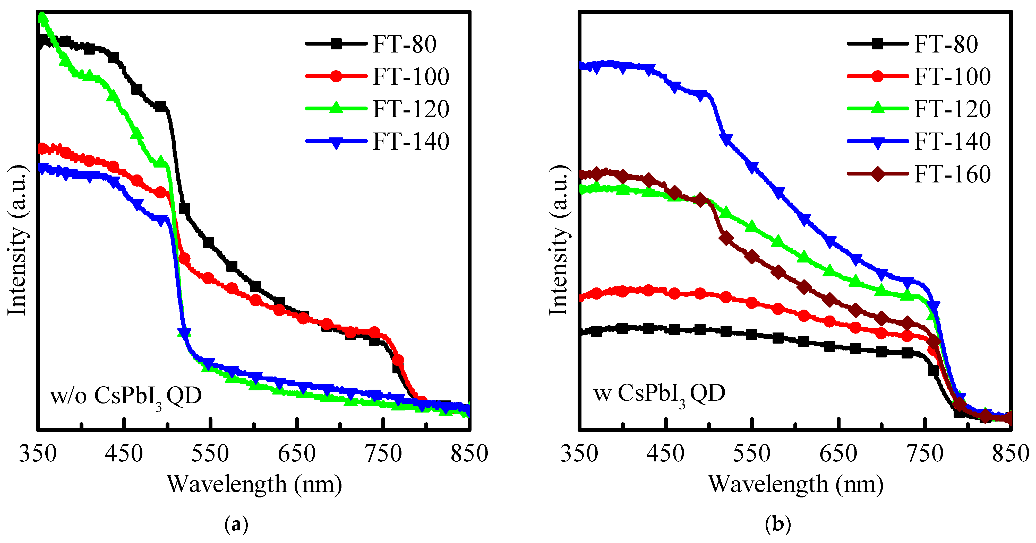
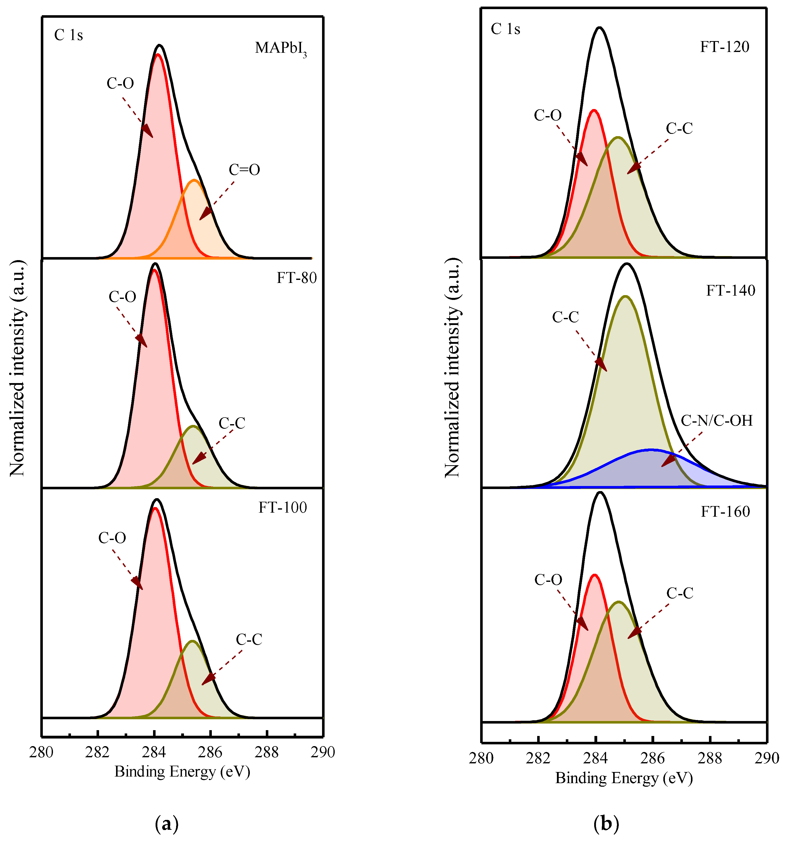
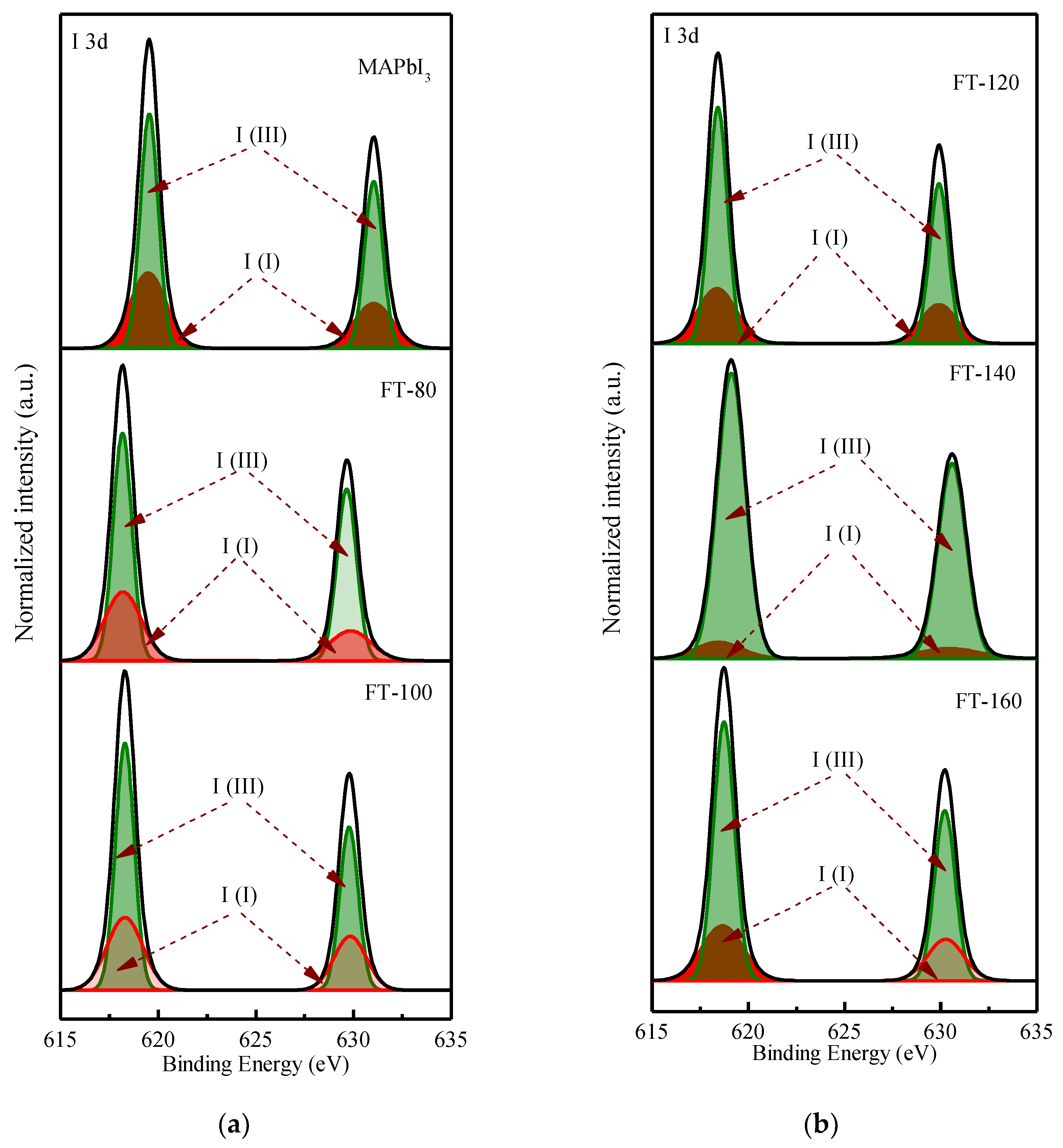
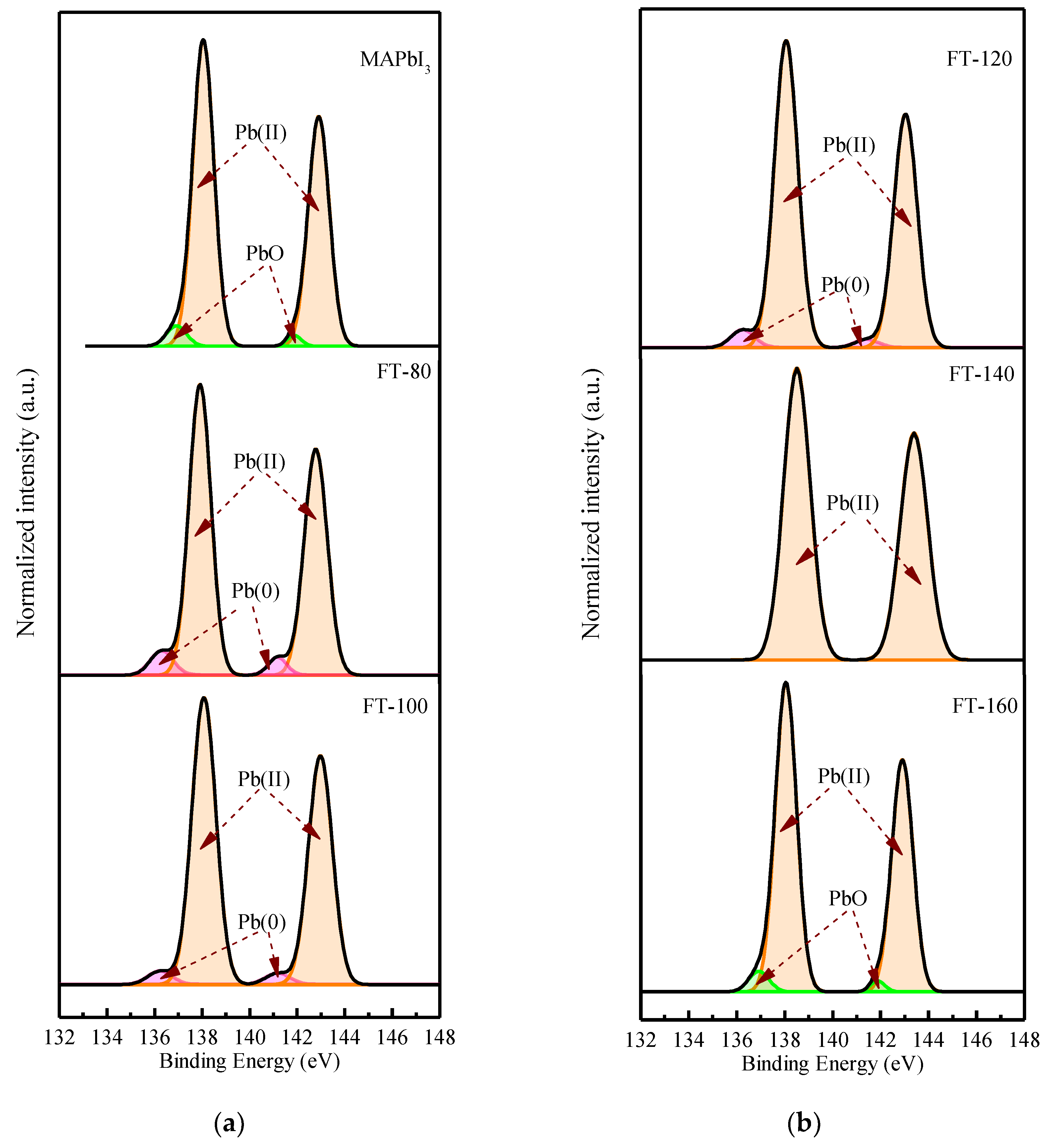
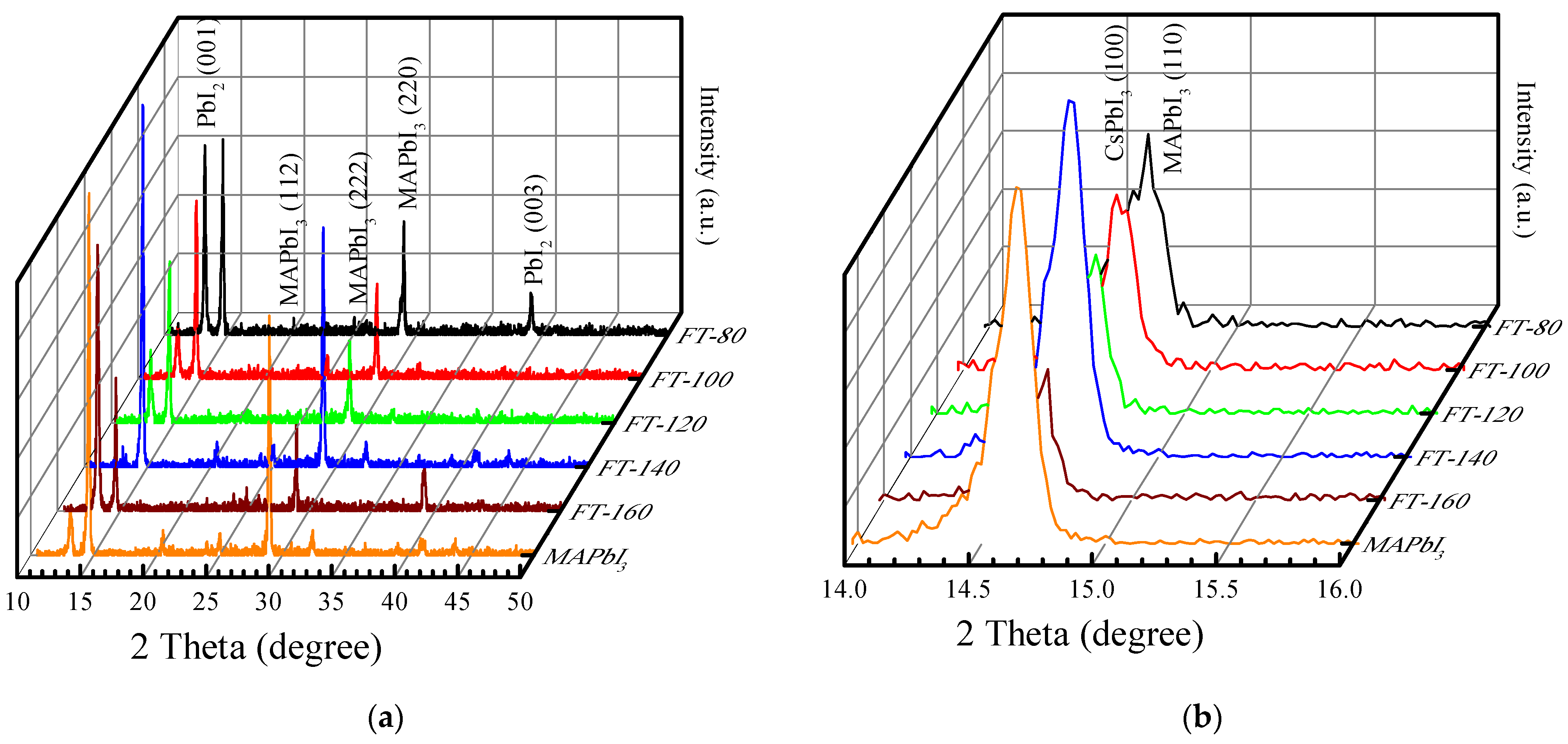
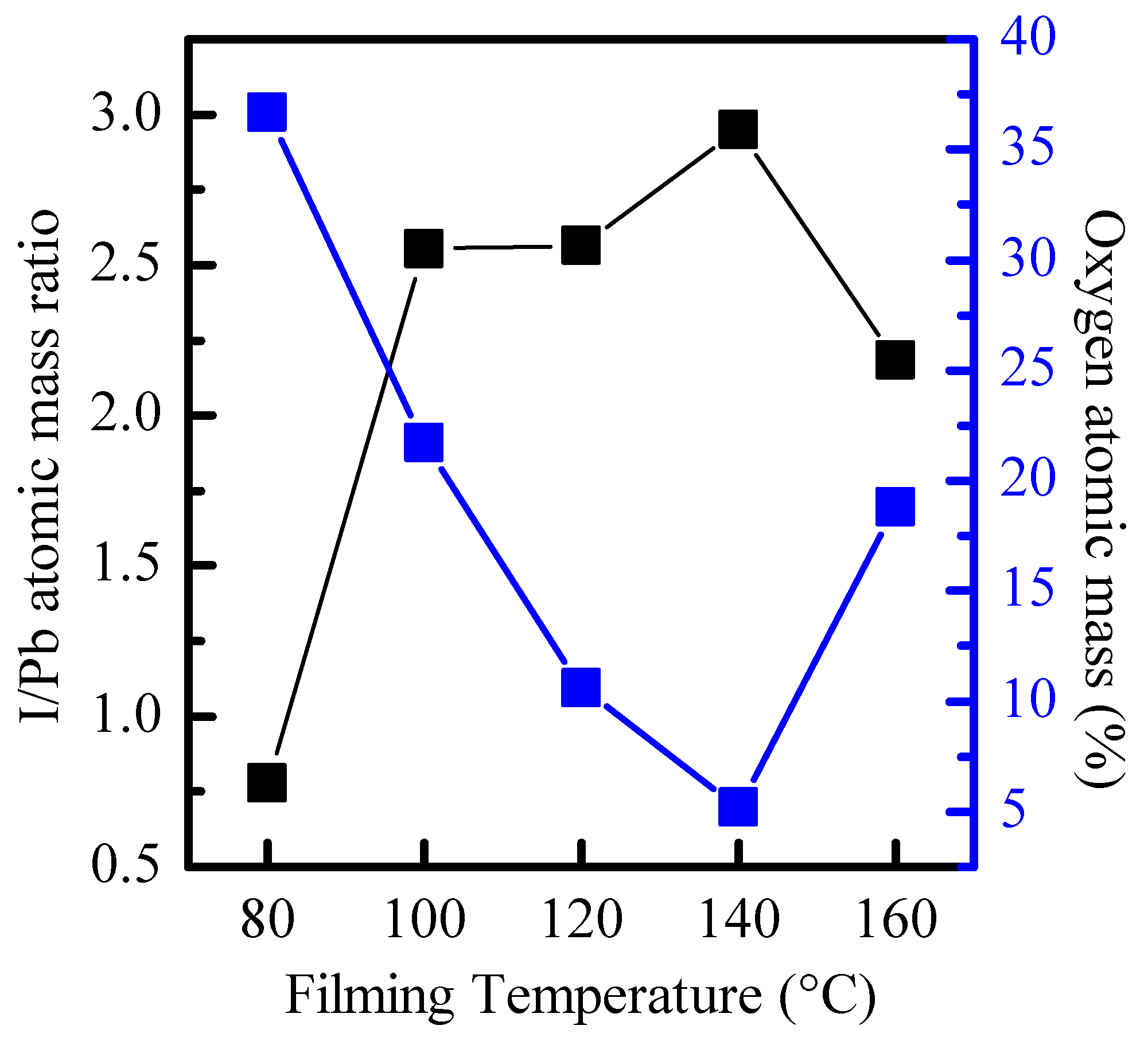
2. Results
3. Materials and Methods
3.1. Materials
3.2. Solution Preparation and Synthesis for Cs-Oleate Precursor, CsPbI3 QDs and CH3NH3PbI3
3.3. Synthesis of Cs-Oleate
3.4. Synthesis of CsPbI3 QDs
3.5. Purification of CsPbI3 QD
3.6. Synthesis of CH3NH3I
3.7. Fabrication of Thin Films
3.8. Characteristic Measurements
4. Conclusions
Author Contributions
Funding
Institutional Review Board Statement
Informed Consent Statement
Data Availability Statement
Conflicts of Interest
Sample Availability
References
- Fakharuddin, A.; De Rossi, F.; Watson, T.M.; Schmidt-Mende, L.; Jose, R. Research Update: Behind the high effi-ciency of hybrid perovskite solar cells. APL Mater. 2016, 4, 091505. [Google Scholar] [CrossRef]
- Glunz, S.W.; Preu, R.; Biro, D. Crystalline silicon solar cells: State-of-the-art and future developments. Compr. Renew. Energy 2012, 1, 353–387. [Google Scholar]
- Kim, H.-S.; Lee, C.-R.; Im, J.-H.; Lee, K.-B.; Moehl, T.; Marchioro, A.; Moon, S.-J.; Humphry-Baker, R.; Yum, J.-H.; Moser, J.E.; et al. Lead Iodide Perovskite Sensitized All-Solid-State Submicron Thin Film Mesoscopic Solar Cell with Efficiency Exceeding 9%. Sci. Rep. 2012, 2, 591. [Google Scholar] [CrossRef] [PubMed] [Green Version]
- Alharbi, E.A.; Alyamani, A.Y.; Kubicki, D.; Uhl, A.R.; Walder, B.J.; Alanazi, A.Q.; Luo, J.; Burgos-Caminal, A.; Albadri, A.; AlBrithen, H.; et al. Atomic-level passivation mechanism of ammonium salts enabling highly efficient perovskite solar cells. Nat. Commun. 2019, 10, 1–9. [Google Scholar] [CrossRef] [PubMed] [Green Version]
- Oga, H.; Saeki, A.; Ogomi, Y.; Hayase, S.; Seki, S. Improved understanding of the electronic and energetic land-scapes of perovskite solar cells: High local charge carrier mobility, reduced recombination, and extremely shallow traps. J. Am. Chem. Soc. 2014, 136, 13818–13825. [Google Scholar] [CrossRef]
- Liu, D.; Yang, J.; Kelly, T. Compact Layer Free Perovskite Solar Cells with 13.5% Efficiency. J. Am. Chem. Soc. 2014, 136, 17116–17122. [Google Scholar] [CrossRef]
- Slimi, B.; Mollar, M.; ben Assaker, I.; Kriaa, I.; Chtourou, R.; Marí, B. Perovskite FA1-xMAxPbI3 for Solar Cells: Films Formation and Properties. Energy Procedia 2016, 102, 87–95. [Google Scholar] [CrossRef]
- Dualeh, A.; Tétreault, N.; Moehl, T.; Gao, P.; Nazeeruddin, M.K.; Grätzel, M. Effect of Annealing Temperature on Film Morphology of Organic-Inorganic Hybrid Pervoskite Solid-State Solar Cells. Adv. Funct. Mater. 2014, 24, 3250–3258. [Google Scholar] [CrossRef]
- Cao, X.; Zhi, L.; Jia, Y.; Li, Y.; Zhao, K.; Cui, X.; Wei, J. Enhanced efficiency of perovskite solar cells by introduc-ing controlled chloride incorporation into MAPbI3 perovskite films. Electrochim. Acta 2018, 275, 1–7. [Google Scholar] [CrossRef]
- Chen, L.-C.; Tien, C.-H.; Tseng, Z.-L.; Ruan, J.-H. Enhanced Efficiency of MAPbI3 Perovskite Solar Cells with FAPbX3 Perovskite Quantum Dots. Nanomaterials 2019, 9, 121. [Google Scholar] [CrossRef] [PubMed] [Green Version]
- Senocrate, A.; Acartürk, T.; Kim, G.Y.; Merkle, R.; Starke, U.; Grätzel, M.; Maier, J. Interaction of oxygen with hal-ide perovskites. J. Mater. Chem. A 2018, 6, 10847–10855. [Google Scholar] [CrossRef] [Green Version]
- Huang, P.H.; Chen, Y.H.; Lien, S.Y.; Lee, K.W.; Wang, N.F.; Huang, C.J. Effect of Annealing on Innovative CsP-bI3-QDs Doped Perovskite Thin Films. Crystals 2021, 11, 101. [Google Scholar] [CrossRef]
- Smith, A.; Mohs, A.; Nie, S. Tuning the optical and electronic properties of colloidal nanocrystals by lattice strain. Nat. Nanotechnol. 2008, 4, 56–63. [Google Scholar] [CrossRef] [PubMed] [Green Version]
- Luo, S.; Kazes, M.; Lin, H.; Oron, D. Strain-induced type II band alignment control in CdSe nanoplatelet/ZnS-sensitized solar cells. J. Phys. Chem. C 2017, 121, 11136–11143. [Google Scholar] [CrossRef]
- Burschka, J.; Pellet, N.; Moon, S.J.; Humphry-Baker, R.; Gao, P.; Nazeeruddin, M.K.; Grätzel, M. Sequential deposi-tion as a route to high-performance perovskite-sensitized solar cells. Nature 2013, 499, 316–319. [Google Scholar] [CrossRef] [PubMed]
- Ma, X.-X.; Li, Z.-S. Substituting Cs for MA on the surface of MAPbI3 perovskite: A first-principles study. Comput. Mater. Sci. 2018, 150, 411–417. [Google Scholar] [CrossRef]
- Rocks, C.; Svrcek, V.; Maguire, P.; Mariotti, D. Understanding surface chemistry during MAPbI3 spray deposition and its effect on photovoltaic performance. J. Mater. Chem. C 2017, 5, 902–916. [Google Scholar] [CrossRef] [Green Version]
- You, J.; Hong, Z.; Yang, Y.; Chen, Q.; Cai, M.; Song, T.B.; Yang, Y. Low-temperature solution-processed perov-skite solar cells with high efficiency and flexibility. ACS Nano 2014, 8, 1674–1680. [Google Scholar] [CrossRef] [PubMed]


| Mobility (cm2/Vs) | Resistivity (cm2/C) | Carrier Concentration (cm−2) | |
|---|---|---|---|
| pristine MAPbI3 | |||
| FT-80 | |||
| FT-100 | |||
| FT-120 | |||
| FT-140 | |||
| FT-160 |
Publisher’s Note: MDPI stays neutral with regard to jurisdictional claims in published maps and institutional affiliations. |
© 2021 by the authors. Licensee MDPI, Basel, Switzerland. This article is an open access article distributed under the terms and conditions of the Creative Commons Attribution (CC BY) license (https://creativecommons.org/licenses/by/4.0/).
Share and Cite
Lien, S.-Y.; Chen, Y.-H.; Chen, W.-R.; Liu, C.-H.; Huang, C.-J. Effect of Growth Temperature on the Characteristics of CsPbI3-Quantum Dots Doped Perovskite Film. Molecules 2021, 26, 4439. https://doi.org/10.3390/molecules26154439
Lien S-Y, Chen Y-H, Chen W-R, Liu C-H, Huang C-J. Effect of Growth Temperature on the Characteristics of CsPbI3-Quantum Dots Doped Perovskite Film. Molecules. 2021; 26(15):4439. https://doi.org/10.3390/molecules26154439
Chicago/Turabian StyleLien, Shui-Yang, Yu-Hao Chen, Wen-Ray Chen, Chuan-Hsi Liu, and Chien-Jung Huang. 2021. "Effect of Growth Temperature on the Characteristics of CsPbI3-Quantum Dots Doped Perovskite Film" Molecules 26, no. 15: 4439. https://doi.org/10.3390/molecules26154439
APA StyleLien, S.-Y., Chen, Y.-H., Chen, W.-R., Liu, C.-H., & Huang, C.-J. (2021). Effect of Growth Temperature on the Characteristics of CsPbI3-Quantum Dots Doped Perovskite Film. Molecules, 26(15), 4439. https://doi.org/10.3390/molecules26154439