Review

Review on the Properties of Boron-Doped Diamond and One-Dimensional-Metal-Oxide Based P-N Heterojunction

Shandong Key Laboratory of Optical Communication Science and Technology, School of Physics Science and Information Technology, Liaocheng University, Shandong 252000, China
*
Authors to whom correspondence should be addressed.
Molecules 2021, 26(1), 71; https://doi.org/10.3390/molecules26010071
Submission received: 30 November 2020 / Revised: 21 December 2020 / Accepted: 22 December 2020 / Published: 25 December 2020

Abstract

:
This review is mainly focused on the optoelectronic properties of diamond-based one-dimensional-metal-oxide heterojunction. First, we briefly introduce the research progress on one-dimensional (1D)-metal-oxide heterojunctions and the features of the p-type boron-doped diamond (BDD) film; then, we discuss the use of three oxide types (ZnO, TiO2 and WO3) in diamond-based-1D-metal-oxide heterojunctions, including fabrication, epitaxial growth, photocatalytic properties, electrical transport behavior and negative differential resistance behavior, especially at higher temperatures. Finally, we discuss the challenges and future trends in this research area. The discussed results of about 10 years’ research on high-performance diamond-based heterojunctions will contribute to the further development of photoelectric nano-devices for high-temperature and high-power applications.

Graphical Abstract

1. Introduction

Metal oxide materials have attracted great attention from the scientific community because of their important technical applications. One-dimensional (1D) nanorods (NRs), nanowires (NWs) and nanotubes (NTs) formed from metal oxides (such as ZnO, TiO2 and WO3) enable fabrication of some specific nanodevices for optoelectronic applications, for instance, photodetectors [1,2], light-emitting diodes (LED) [3], and solar cells [4,5]. This is because of the large surface-area-to-volume ratio, excellent charge carrier transport performance and good crystallization ability shown by these types of nanostructures [6,7]. Thus far, heterostructure optoelectronic devices have been formed by depositing n-type metal oxides on various p-type substrates, including Si [8,9,10,11], GaN [12,13,14], NiO [15], Cu2O [16,17,18,19], graphene [20,21], boron-doped diamond (BDD) film [22,23,24,25,26,27], and organic material [28]. Among them, BDD acts as an excellent p-type conductive material for high-temperature, high-power and radiation-proof photoelectronic devices with its large band gap at room temperature (5.47 eV) and high thermal conductivity [29]. When combining 1D metal oxide with p-type diamond, one has to explore the carrier transport behavior of the formed heterojunction devices, which has both theoretical and application importance for designing new photoelectronic devices for extremely harsh environments, such as outer space or nuclear energetics industries. In recent years, p-type BDD has been used in combination with various 1D-structured metal oxides (for instance ZnO [22,30,31,32,33], WO3 [34,35,36] and TiO2 [37,38,39,40,41]) to form heterojunctions demonstrating effects of rectification and negative differential resistance (NDR), which may be widely used in various technologies. However, no comprehensive discussion focusing specifically on electrical characteristic of diamond-based p-n heterojunctions has been published. Therefore, this review summarizes the past progress in the device fabrication, electrical transport properties and NDR-related applications of diamond-metal oxides (ZnO, TiO2 and WO3) heterojunctions. The temperature-driven carrier injection mechanisms in such heterojunctions are described herein in further detail. The approximately 10 years of research discussed will benefit the next step in the development of high-temperature and high-power optoelectronic devices.

2. Heterojunctions with 1D Metal Oxides Semiconductors

Since the discovery of carbon NTs by Professor Iijima in 1991 [42], 1D nanomaterials have quickly become one of the hotspots in the research of nanomaterials and functional devices. Carbon NTs have excellent physical and chemical properties, such as large surface-area-to-volume ratio, high mechanical strength and brilliant thermal conductivity, as well as good chemical stability. However, the use of presently existing growth technologies does not allow a readily available effective chiral control over the synthesis of carbon NTs [43], always resulting in a compound with both metallic and semiconducting properties. As such, it is impossible to obtain a completely pure semiconductor, which greatly limits the applications of optoelectronic devices.
Because of the above limitation, researchers started with the development and investigation of other 1D semiconductor nanomaterials. Silicon (Si) is the most widely used semiconductor material for optoelectronics devices. Professor Charles Lieber of Harvard University, as the leading expert in this field, for the first time has successfully prepared Si NWs [44] and employed them in photovoltaic sub-devices, biosensors, etc. [45,46], showing the revealed nanomaterials and devices to have broad-range expectations in engineering.
However, Si NWs also demonstrate some shortcomings, such as easy oxidation to form polycrystalline or crystal defects in air, which may have a prevailing effect on the electrical transmission characteristic. Due to this fact, researchers reoriented to the development and implementation of 1D nanometer semiconducting materials with less oxidizing ability and higher stability. In 2001, the discovery of metal oxide semiconductor nanobelts pushed the study of nanomaterials forward to a new challenge. Metal oxides as the prime candidates for new functional inorganic materials are finding many promising applications in aerospace, biological engineering, semiconductor electronics, functional ceramics, and other fields. The 1D metal oxide nanosystems belong to the most prominent examined systems due to their good crystal quality, low defect density, excellent charge-carrier mobility, and fast response [47], thereby forming a promising replacement for traditional silicon-based electronic and optical devices.
The most recent studies have reported on the excellent optical–electronic performance of 1D metal oxides as well as new functional devices based on various substrate materials. Du et al. prepared a high-speed ultraviolet photoelectricity detector of ZnO-NWs Schottky barrier based on the surface-ionic-gate powered by tribo-nanometer generator [48]. Wang et al. demonstrated a novel bipolar response in self-powered ZnO NWs/Sb2Se3 heterojunction photodetector with adjustable polarity switching wavelength. As demonstrated in Figure 1, the output signal shows the change in the photocurrent polarity between shorter (405 nm–690 nm) and longer (760 nm–880 nm) wavelength regions [49]. Gao et al. have recently obtained a UV-free white LED based on high-level Fe-doped p-ZnO NWs arrays on the n-GaN substrate [12]. Peng et al. developed a real-time wearable UV-radiation monitor by exploiting the excellent properties of p-CuZnS/n-TiO2 photodetector [50]. Tang et al. proposed a feasible way to improve the hole doping in ZnO:N films with introduced beryllium and demonstrated strong near-band edge UV emission of the ZnO homojunction LED devices, which can be observed even at 400 K under continuous current injection [51]. Ye et al. improved the performance of n-ZnO NRs/p-GaN LED with the use of transparent graphene electrode. The transparent graphene electrode was used as the current diffusion layer, showing better performance compared to that in the ITO analogs [52]. The photoelectrochemical self-powered photodetectors related to ZnO/CdS NWs were manufactured by Zhang’s group [53]. The ZnO NWs were used as the carrier collection channels and UV absorbers with a well-organized structure to efficiently absorb light, whereas CdS nanoparticles were used as the visible photosensitizers. Prepared ZnO NWs/CdS structures demonstrate superfast response time and effective sensitivity to visible light and UV in the absence of power.
Cheng et al. fabricated a SnS/TiO2 NTs arrays photoelectrode synthesized by anodization combined with electrodeposition technique, which was used to degrade 2,4,6-trichlorophenol under simulated visible light irradiation [54]. Yan et al. prepared photocatalytic binary composite MoS2/TiO2 (NTs) heterojunction (Figure 2). The composite material has demonstrated good photocatalytic disinfection effect and recyclability and as such has a broad field of potential applications in water disinfection [55]. Gu et al. reported on the preparation of novel WO3 NRs/graphene/BiV1−xMoxO4 heterojunction photoelectrode for photoelectrochemical water splitting. The heterojunction exhibits an enhanced photocurrent density, which makes light conversion efficiency significantly improved [56].
Specifically, these studies provide new strategies and insights for the fabrication of high-efficiency optoelectronic devices. One may see that most of the existing 1D metal oxide heterojunctions are generally based on Si, GaN and Cu2O, etc., and such devices show excellent photoelectric performance under normal environmental conditions. However, due to the small size of nanostructures, both light and injection current will cause a significant thermal effect. Since the thermal conductivity of the listed substrates is low, it leads to the rise in the thermal noise phenomenon and fluctuation of the effective barrier height at a high temperature. With the temperature rise, an increase in the leakage current, a drift of the threshold voltage and enhanced thermal noise degree will affect the sensitivity and reliability of the device. In addition, there is a large thermal coefficient difference between the metal oxides and the Si substrate. The interface between these two materials plays an important role in the device performance: the heterogeneity at the interface will cause the effective barrier height to fluctuate with the reduced performance of a device. This phenomenon is more evident in harsh environments such as high temperature and high flux [57,58,59].

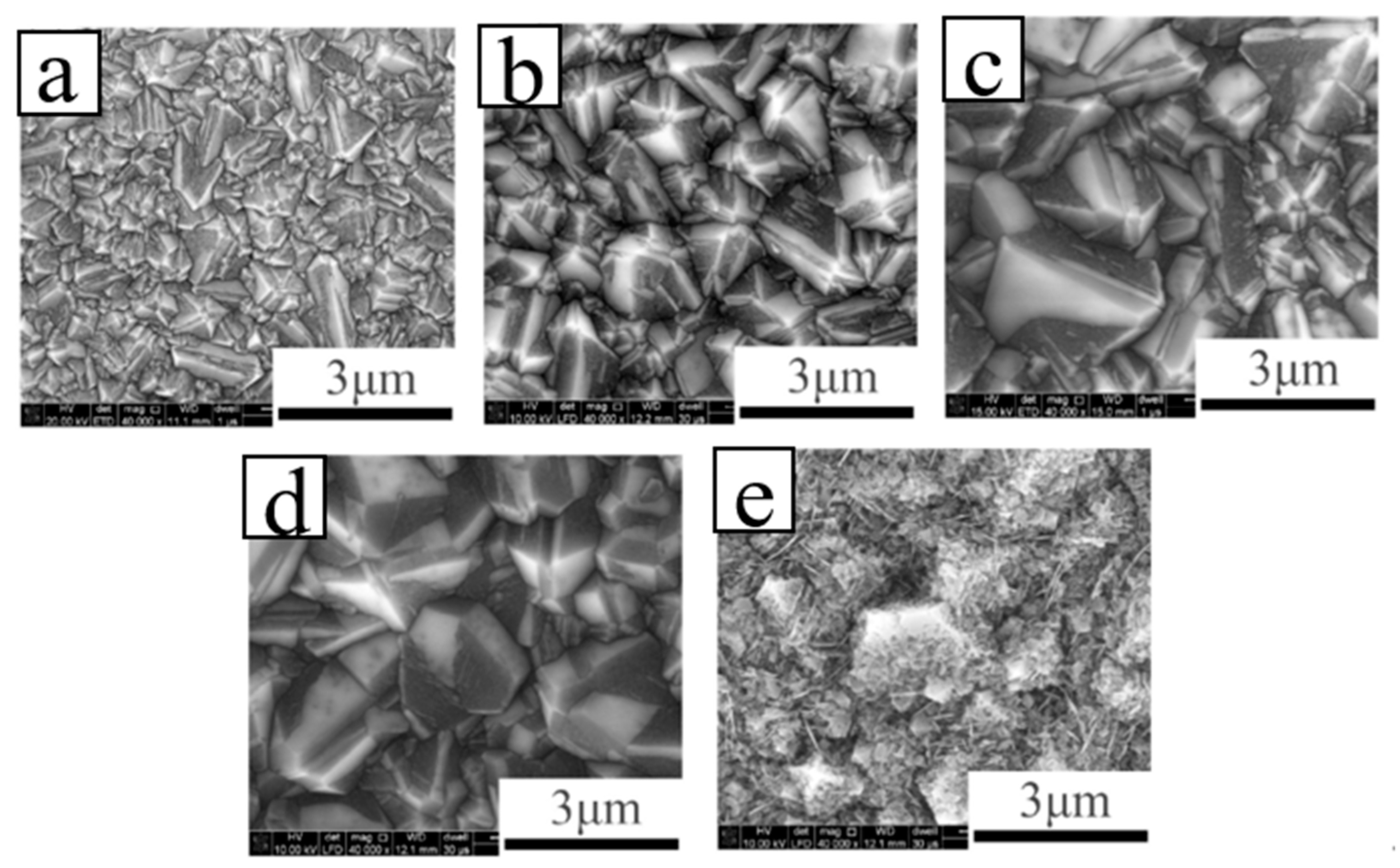
3. P-Type B-Doped Diamond Films

Compared with other wide band gap semiconducting substrates (NiO2, GaN, SiC, etc.), diamond has favorable intrinsic optoelectronic performance, for instance, high thermal conductivity (22 W·cm−1·K−1), high carrier mobility (2200 and 1800 cm2·V−1·s−1), high electrical breakdown field (10 MV·cm−1) and high saturation velocity (2.7 × 10⁻⁷ cm·s−1) [60,61]. Therefore, diamond is regarded as a suitable material for high power and high temperature to cooperate with metal oxide semiconductors in optoelectronic devices. So far, the main requirements include high-quality epitaxial growth as well as doping. However, because of the contradiction between structural quality and the electrical properties of p-diamond, it is still a challenge to produce high-quality p-type diamond structures. With boron doping, diamond can be transformed from an insulator into a semiconductor or even a superconductor, wherein a boron atom is in the form of a host impurity in the diamond. High-boron doping in the diamond film may enhance its electrical resistivity (up to 10−3 Ω·cm order). In order to improve the efficiency of B-doping pursuing high mobility and high crystal quality, many efforts have been implemented.
Experimentally, Li’s group obtained the BDD film synthesized by hot filament chemical vapor deposition (HFCVD) [62]. B(OCH3)3 was utilized as the boron doping source in a methane (CH4) and hydrogen (H2) reaction atmosphere with a flow rate of 0, 2, 5, 10 and 20 sccm. The resistances decrease for the B-doping diamond films grew with increasing the H2 flow rate tested by Hall-effect measurement. The undoped diamond film consists of pyramid-shaped grains. With the increase of the B-flow rate up to 2 sccm and 10 sccm, the majority of grains showed lamellar-shaped twin characteristic, on account of the renucleation induced by B-doping. As for 20 sccm, the grains showed a dominating pyramid-shaped morphology, and a twinned crystal appeared (Figure 3). Raman spectroscopy (Figure 4) is an effective technique to investigate the structure of doped diamond. It is worth noting that owing to the high content of BDD, the p-degenerated diamond peak (1332 cm−1) shows an asymmetric curve and shifts towards the lower wavelength values in the region-centered phonon bands. Moreover, two wide bands that appear at 500 cm−1 and 1200 cm−1 in the low-frequency spectrum portion are consistent with two maximum values of phonon density in the diamond state.
In the most recent study [63], a small amount of sulfur was added during the deposition of BDD films by microwave plasma chemical vapor deposition (MPCVD), as reported by Liu’s group. The results show the highest values of at once doping efficiency, growth rate, hole mobility and concentration, crystal mass and surface morphology of boron attained with the addition of sulfur (Figure 5). In the presence of an appropriate amount of sulfur, a high carrier concentration of 1.2 × 10¹⁹ at/cm3 may be obtained during the growth process when the B-C ratio is only 2.5 ppm, which denotes a high efficiency of boron doping. The regulation mechanism of sulfur addition has been considered in terms of sulfur-induced plasma changes and possible boron-sulfur complex formation.
Wei et al. [64] reported on the B-doped double-layer diamond films fabricated by MPCVD and discussed the influence of B-doping concentrations on the surface morphology, crystal quality, surface composition, conductivity and secondary electron emission properties. With increasing boron doping amount, the conductivity becomes beneficial to the emission of secondary electrons. However, as a consequence of the declining quality of the diamond crystals (Figure 6), the increased sp2 carbon on the surface and the boron segregation on the surface will reduce the effects of secondary electron emission in the films. Therefore, this improves vertical conductance, which increases the escape depth of secondary electrons and obviously leads to the reduced surface performance with the B doping. The results show that the films with the boron-doped layer demonstrate a low concentration of the crystals with excellent quality and sufficient conductivity, which helps to attain the outstanding properties of the secondary electron emission.
Specifically, the discussed results referring to BDD demonstrate strategies for improving the doping efficiency, hole mobility, carrier concentrations, conductivity and the diamond crystal quality to further provide an efficient way to grow high-quality p-diamond material, restoring its lattice mismatch and demonstrating potential for p-BDD-based applications in optoelectronics.

4. Diamond-Based 1D Metal Oxide Heterojunction Classes

The combination of metal oxide and BDD has attracted wide attention, the main reason for which is the lack of effective n-type doping in diamond and p-type doping in metal oxide. The configuration of p-BDD and n-metal oxide has been most widely studied. In contrast to a continuous uniform film [26,27,32,65,66,67,68,69,70,71,72,73], the 1D nanostructure (e.g., NRs, NWs and NTs) that is free of defects, quantum-enhanced and has a large surface-area-to-volume ratio will not encounter the thermal mismatch with diamond, thereby substantially improving the performance of the hybrid structural heterojunction. For simplicity, we will focus on three different 1D n-type metal oxide (ZnO, TiO2 and WO3)/p-BDD heterojunction structure types in this review in the following general examples.

4.1. D N-ZnO/P-Diamond Heterojunction

ZnO is a suitable unintentionally doped n-type semiconductor with the wide band gap of 3.7 eV and exciton binding energy as high as 60 meV, which is promising for a wide range of applications. Various forms of ZnO nanostructures, such as NWs [15], NRs [74], nanobelts [75] and nanosheets [76], have been commonly studied because of their favorable optoelectronic performance compared with the bulk material. In these nanomaterials mentioned above, 1D n-ZnO nanostructures are supposed to be the most efficient for optoelectronic diodes owing to their high-density surface trap states, fewer interference states, excellent carrier confinement and grain boundaries [77]. They are able to improve the optoelectronic performance of photodiode devices [6,78].

4.1.1. Epitaxial Growth of 1D ZnO NRs/Diamond Facet

At room temperature and normal pressure, ZnO shows the hexagonal wurtzite structure (Figure 7). Each Zn2+ ion is surrounded with four O2− ions corresponding to tetrahedral coordination (sp3 orbital hybridization) corresponding to the C6V4 class and P63mc space group. The shape of Zn2+-O2− tetrahedrons, as well as the ionic–covalent nature of Zn-O bonding, define the intrinsic polarity in the ZnO crystal growing along the c-axis [0001] orientation. Therefore, various 1D nanostructures are readily formed in the ZnO growth process [79].
Diamond is a typical atomic crystal with a face-centered cubic structure, belonging to the equiaxed crystal system. The carbon atoms in the diamond structure are bonded by sp3, with each carbon atom being bonded with four adjacent carbon atoms. The arrangement of diamond carbon atoms is shown in Figure 8, which contains a carbon atom centered in a regular tetrahedron and a carbon atom at each of four vertices, wherein carbon atoms at each vertex are covalently bonded with C-C bonds and shared by four tetrahedrons to form a three-dimensional network of diamond crystal [80].
In terms of theoretical background, Li’s group proposed the epitaxial growth mechanism for the structure of ZnO-diamond. Since both ZnO crystal (0001) facet and diamond (111) facet have the same hexagonal atomic arrangement, ZnO (0001) planes and diamond (111) are geometrically matched. The [0001] oriented 1D ZnO NRs are normally aligned and epitaxial grown perpendicular to the diamond (111) plane. The epitaxial growth relation between the ZnO (0001) and diamond (111) is suggested in compliance with (0001) [11 2 ¯ 0]ZnO//(111)[1 1 ¯ 0] diamond or (0001)[10 1 ¯ 0]ZnO//(111) [1 1 ¯ 0]diamond (Figure 9a), and the epitaxial growth relation between the (0001) ZnO and (100) diamond is primarily of (0001)[0001]ZnO//(101) [101] diamond (Figure 9b) [23]. An in-depth study of 1D ZnO/diamond system will not only contribute to understanding the physical mechanism for epitaxial growth but also to extending the area of ZnO/diamond applications in optoelectronics devices.

4.1.2. 1 D N-ZnO/P-Diamond Related Optoelectronic Devices

In the past, the existing ZnO types were usually deposited on a diamond substrate in the form of thin-film, which was used for surface acoustic wave (SAW) filters applications [65], examining structural and electrical properties [66,67,72], and for constructing p-n junction diode [68]. In the last ten years, composite 1D ZnO related-nanostructures and diamond nano-optoelectronic p-n junction devices were extensively studied. Zhi et al. [69] developed novel tyrosine biosensor with the biological function based on ZnO NRs on the BDD substrates. The ZnO NRs were for the first time deposited on BDD thin film by a low-temperature solution method. Boron-doped ZnO nanorods were fabricated on the BDD by hydrothermal technique and showed high photocatalytic performance [33]. Gao et al. [81] reported on photocatalytic activity of the n-ZnO NRs/p-BDD heterojunction fabricated with the hydrothermal degradation of methyl orange dye, which depended on the density and diameter of ZnO NRs, the distance between NRs and the interface at ZnO-BDD heterojunction (Figure 10). Vertically aligned ZnO NRs were synthesized by Wang et al. [82] for the first time by using a low-temperature solution method on the BDD films. The heterojunction showed typical rectification characteristics with the standard ideality factor approaching theoretical values under both low and high forward-biasing voltages (Figure 11).
In recent years, ZnO NRs/BDD have been prepared and used as an anode for photocatalytic oxidation of aniline. The results showed that ZnO NRs/BDD is a promising photoanode for organic degradation [83]. Huang et al. [84] proposed a low-temperature annealing process to improve the optical response of the ZnO NRs/nano-diamond film substrate for the UV photodetector. Furthermore, novel ZnO NRs/ultra-nanocrystalline diamond may be used as a high-sensitivity device for hydrogen gas sensing (Figure 12) [85]. They also reported ZnO NTs, with the diamond NWs enhancing UV detection and field emission properties [86].
Compared to n-ZnO NRs/p-BDD heterojunction, n-ZnO NWs/p-BDD heterojunction reported by Sang et al. shows better I-V electrical properties and higher electrical transport performance (Figure 13 and Figure 14) [30]. By comparing both dark and UV illuminated I-V characteristics, one may see that the UV illumination reduces the turn-on voltage and ideality factor of the tested heterojunction. At 10 V, the UV positive current is more than 4 times as much as the dark [31]. To sum up, the high UV response rate, long device life and fast switching speeds of the heterojunction make it an ideal material for multifunctional optoelectronic applications.

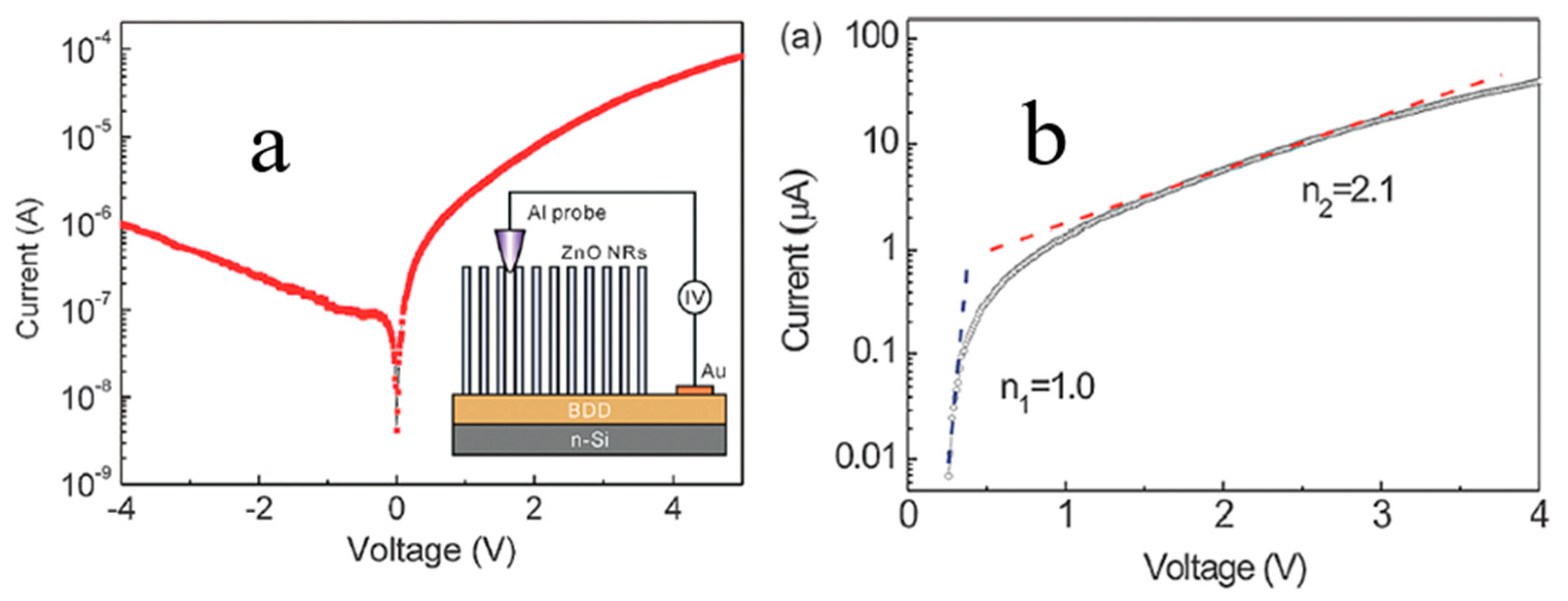
4.1.3. Electrical Transport Behavior of N-ZnO NRs/P-BDD Heterojunction at Elevated Temperatures

Both diamond and ZnO are significant high-temperature materials, so the behavior of n-ZnO/p-BDD system is investigated at elevated temperatures. Sang et al. [24] reported on the preparation progress of n-ZnO NRs/p-BDD heterojunction devices and their electrical transport behavior in the temperature range from 25 °C to 220 °C. The device exhibits representative rectifying behavior at all test temperatures (Figure 15). The turn-on voltage of heterojunction decreases at higher temperatures. This is due to the fact that at higher temperatures, more holes are produced on the BDD side. The conductivity was lower than that of n-ZnO NRs/p-Si heterojunction [87], indicating that n-ZnO/p-BDD-based devices have better electrical properties at high temperatures. The decrease of n at higher temperatures is due to the increasing number of thermally excited carriers, the enhanced barrier tunneling, and the recombination process in the depletion region. At higher temperatures, both the carrier injection and ohmic behavior are improved. The detection temperature of n-ZnO NRs/p-BDD reaches about 220 °C, which is currently the maximum temperature for the p-n heterojunctions based on n-ZnO NRs.

4.1.4. NDR for 1D N-ZnO/P-Degenerated BDD Heterojunction at Elevated Temperatures

When p-diamond is degraded by heavy boron-doping (higher carrier concentration, 1020 orders of magnitude), the heterojunction exhibits the NDR phenomenon. The n-ZnO/p-degenerated BDD heterojunction provides a new way to form an NDR tunneling diode. The NDR phenomenon of 1D n-ZnO NRs/p-degenerate BDD was observed by Li et al. [23], and the forward I-V plots can be divided into three regions. The NDR phenomenon occurs with the peak-valley current ratios (PVCR) of ~10 (Figure 16a). The generation of NDR is caused by the tunneling current in the ZnO and p-degenerated BDD structures.
In our most recent study [31], we reported on n-ZnO NRs/p-degenerated BDD tunnel diode and its NDR characteristics with temperature change as well as carrier tunnel injection behavior. The results show that the prepared heterojunction exhibits NDR performance at 20 °C and 80 °C. Subsequently, NDR disappears, and rectifying properties become visible at 120 °C (Figure 16b). The PVCR is reduced at higher temperatures. The tunneling current from diamond valence states to ZnO deep levels leads to the reduction in the turn-on voltage at higher temperatures and promotes the appearance of NDR. The high-temperature NDR phenomenon of 1D n-ZnO NRs/p-degenerated BDD heterojunction may extend the resistance switches and resonant tunneling diode applications to high-temperature and high-power environments.
Table 1 provides an overview of a portion of recent investigations based on 1D n-ZnO/p-diamond heterojunction for various applications and properties.

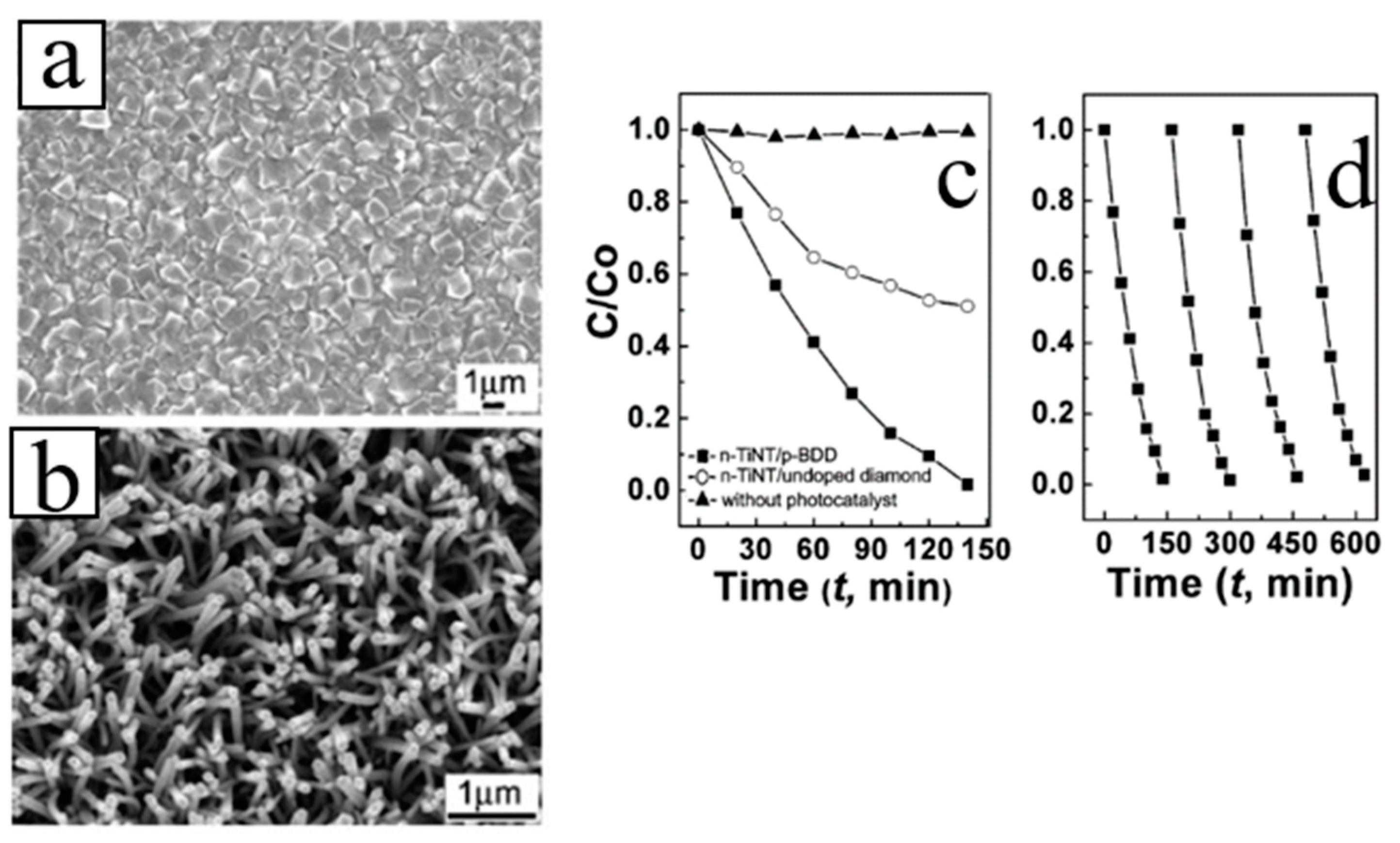
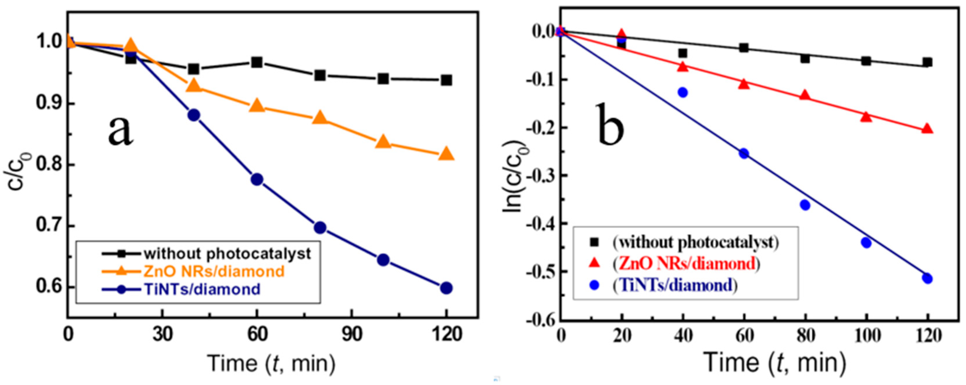
4.2. 1 D N-TiO2/P-Diamond Related Optoelectronic Devices

1D TiO2 nanostructures with a wide bandgap (3.2 eV) and a large surface area [88] were selected as a promising material for application in electronics [89,90,91]. Common functional TiO2 nanomaterials have attracted widespread attention due to superior performance derived from their inherent 1D architecture [92,93,94]. 1D nanostructures offer more possibilities for better optical and electrical properties, such as faster carrier generation, better charge separation, and longer charge carrier life [95,96,97]. TiO2 is an intrinsic n-type semiconductor and may form a p-n heterojunction combined with the p-type semiconductor [98,99,100,101,102]. N-type TiO2 and p-type BDD have excellent and unique properties, which make them ideal semiconductors for forming heterojunction structures.
In their previous study, Li et al. [103] deposited 1D TiO2 NRs with different morphology grown on BDD film with ZnO layer using the hydrothermal method. TiO2 NRs/ZnO/BDD heterojunction may enhance the photocatalytic activity of TiO2 NRs/ZnO and TiO2 NRs/BDD heterojunctions, respectively. In addition, TiO2 NTs arrays were fabricated on the p-type BDD substrate by means of liquid phase deposition using ZnO NRs template. Compared with the case of a single TiO2 NTs, n-TiO2 NTs/p-diamond heterostructure shows significantly enhanced photocatalytic activity and good recyclability (Figure 17) [38,39]. Afterward, TiO2 NTs were deposited by the same method on hemispherical CVD diamond films. The degradation of reactive yellow 15 (RY15) solution showed that the product exhibits high photocatalytic performance (Figure 18) [104].
TiO2 NTs/BDD composite electrode (Figure 19a) was fabricated by microwave plasma-enhanced chemical vapor deposition (CVD) by the Siuzdak group, which greatly enhanced the electrochemical properties. Compared with the BDD prepared on a Ti plate (0.11 mF·cm−2), the composite electrode provides high capacitance (Figure 19b). The enhanced capacitive effect in TiO2 NTs/BDD can be understood as follows: (1) the particular cooperative morphology of TiO2 NTs and BDD provides a more efficient conduction route for ion diffusion; (2) NTs are partially decomposed and converted to Ti2O3 and TiC fractions. Finally, TiO2 NTs, which demonstrate high ordering attained by a simple, rapid and controllable anodic oxidation method, can be used as the conductive BDD layer deposited on a substrate and then embedded into the structure of a supercapacitor [70,105,106].
Most recently, Miroslav et al. [41] reported on the development of a unique photoelectrochemical electrode consisting of a nanostructured BDD layer covering an n-type TiO2 film (Figure 20). The effects of the nanostructure, B doping level and TiO2 film thickness on the properties of PEC were studied. Using RF magnetron sputtering, the BDD films with two doping levels (gas phase B/C = 1000 ppm and 10,000 ppm) that had already grown and plasma-nanostructured were used as the substrates to deposit TiO2 layers of 20, 100 and 500 nm. BDD was used as the structure electrode. When the gas phase B/C ratio was 1000 ppm, the surface was covered with a TiO2 layer 500 nm thick, and the photocurrent was the highest (60 μA/cm2 and 3.2 mA/cm2 at 0 and 2 V vs. Ag/AgCl respectively). The favorable influence of the nanostructure type and pn junction on the hole injection was confirmed by experiments. Suzuki et al. [37] prepared a mesoporous TiO2 layer on the BDD and found that deep-UV illumination could improve its photocatalytic efficiency. They also used this hybrid electrode in water electrolysis to produce O3 gas and other reactive oxygen species (ROS). In addition, ROS produced by electrochemistry were tested in water treatment under UV illumination and demonstrated the system’s suitability for advanced oxidation processes [27]. This simple water treatment system can be used to break down refractory organic matter in wastewater, a process that is still being studied. Basically, the 1D n-TiO2/p-BDD device suggests a new strategy, which is expected to be used for its wide-range implementation in photocatalysis, photoelectric chemical electrode and sensor, etc.
A summary of different synthesis routes and applications (properties) of 1D n-TiO2/p-diamond heterojunction is presented in Table 2.

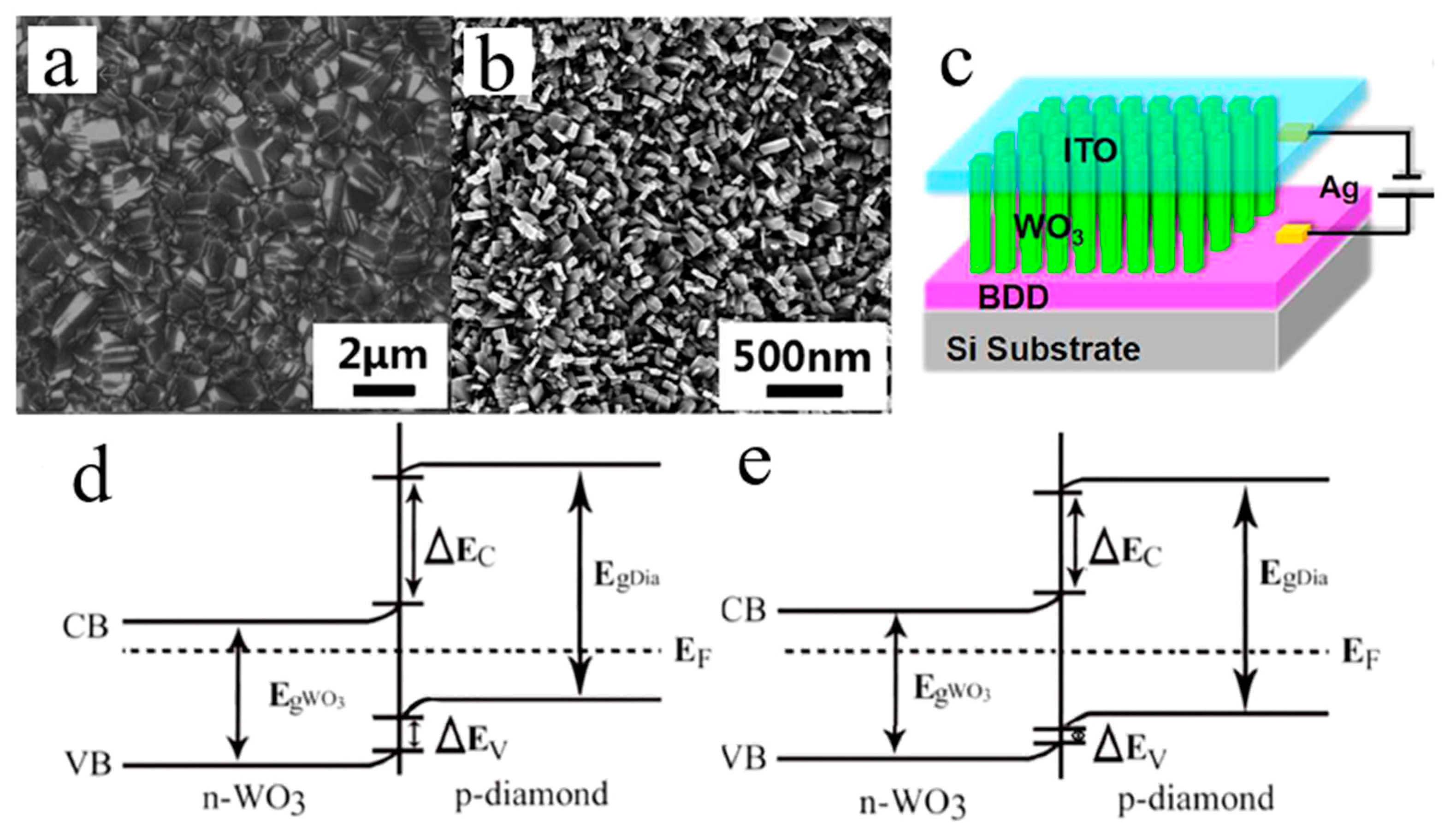
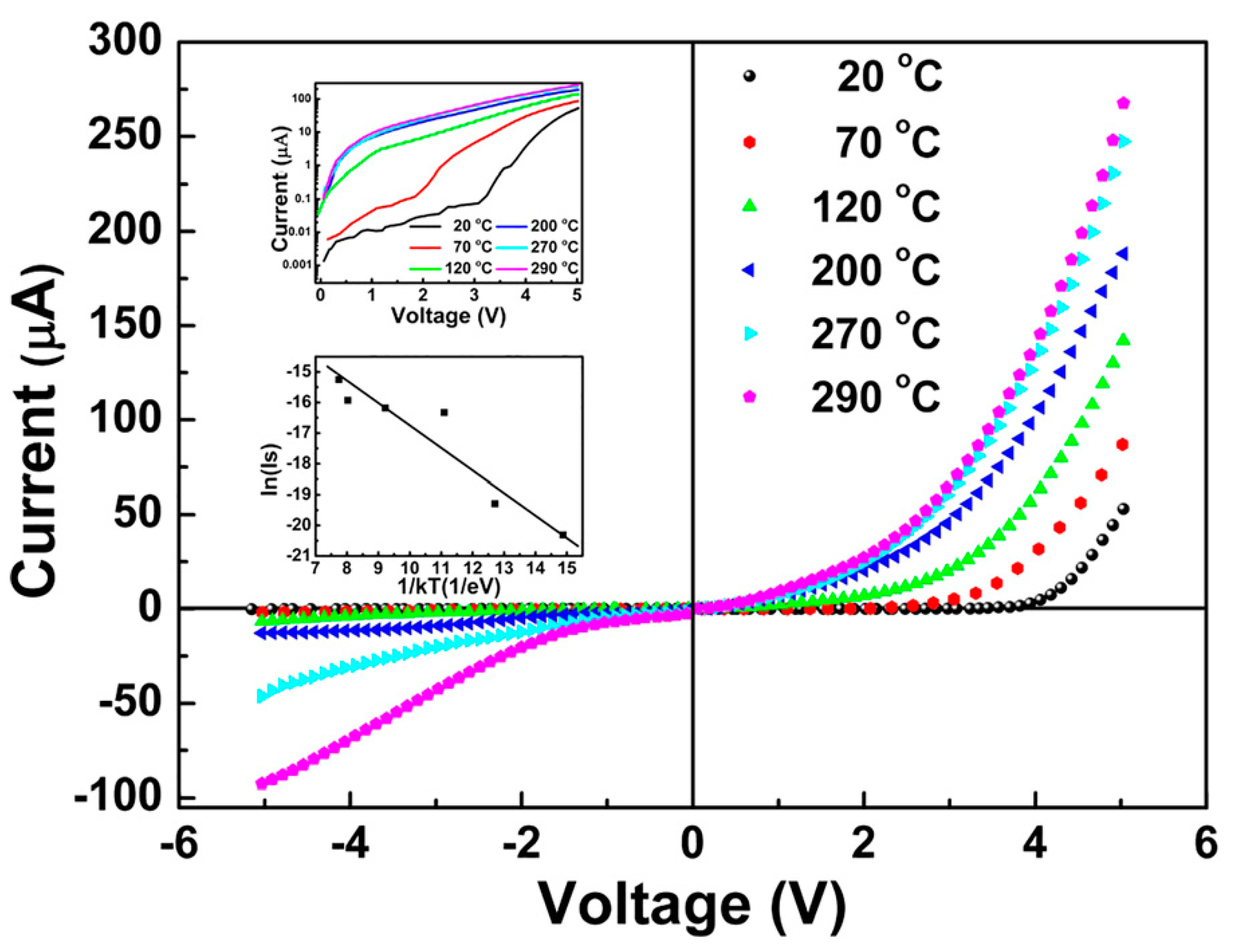
4.3. 1D N- WO3/P-BDD-Related Optoelectronic Devices

WO3 is a low-cost metal oxide semiconductor with a wide band gap (2.7 eV), excellent electron transport and unintentionally n-type doping performance. WO3 is considered as another candidate material for applications in electronics [7,107]. 1D WO3 nanostructures (such as NRs, NWs and nanoneedles) have been used in photocatalytic applications [108,109], sensor switching devices [110], gas sensors [111,112] and UV photodetectors [2]. Because of the excellent performance of 1D WO3 and BDD, it is worth combining them in 1D n-WO3/p-BDD heterojunction to provide new applications in electronics, especially at higher temperatures.
In 2017, Li et al. [34] studied the high-temperature electrical transport behavior of n-WO3 NRs/p-BDD heterojunctions fabricated by the hydrothermal method. WO3 NRs with a square feature of the top surface were deposited onto the BDD with perpendicular alignment to the substrate plane (Figure 21a–c). The p-n heterojunction demonstrated excellent thermal stability and rectified characteristics within the temperature range from room temperature to 290 °C. The turn-on voltages declined, and the rectified ratio was relatively high with the temperature increase. The ideality factor decreases with the increase in temperature (Figure 21b). Under the influence of high temperature, when the reverse voltage is large, both the forward current and the reverse leakage current increase (Figure 22).
At elevated temperatures, the EF value of the heterojunction semiconductor usually moves close to the middle region of the bandgaps (shown in the energy band diagrams, Figure 21d,e) [113]. More intrinsic carriers are thermally excited, and it becomes easier for electrons (holes) to pass from the n-WO3 conduction band (p-BDD valence band) to the p-BDD conduction band (n-WO3 valence band) under the voltage applied, which leads to the decreasing turn-on voltage, increasing forward current, and slightly improved injection efficiency. At higher voltages and for temperatures above 200 °C, the traps are filled with more thermally excited carriers, and the injected current complies with the trap-free SCLC law, with an exponential power of about 2. The Et value of the characteristic trap energy obtained from the heterojunction is 50 meV (inset of Figure 22). The characteristic trap energy values measured for ZnO NRs/BDD heterojunction [24], amorphous polymer semiconductor [114] and organic heterojunction [115] are higher than the listed value.
Compared with the previously reported heterojunctions comprising WO3 (n-WO3/p-carbon NTs [116] and WO3/SnO2 [117]), the structure of 1D n-WO3/p-BDD has better electrical transport performance at higher temperatures. This study extends the ranges of the design and application for heterojunctions based on BDD, especially their employment at high temperatures, high power and in various harsh environments.

5. Conclusions and Future Perspective

In this review, we have summarized recent general findings for diamond-based metal oxide p-n heterojunctions, especially those that comprise three important types of 1D nanostructures studied in this photoelectric decade. The features of p-type BDD films and corresponding epitaxial growth relationships of 1D ZnO NRs on diamond facet have been experimentally and theoretically predicted. High-temperature electrical transport behavior and NDR of n-ZnO NRs/p-BDD heterojunction have been presented in detail. 1D n-TiO2/p-BDD heterojunction-related optoelectronic applications, including photocatalysis and photoelectrochemical electrode, have been presented. The fabrication of 1D n-WO3/p-BDD heterojunction and its electronic behavior at high temperature are discussed.
These above-mentioned reports provide a greatly expanded understanding of the background of electrical properties in diamond-based 1D metal oxides p–n heterojunctions. In the future, it is also desirable to find new fabrication routes and types of electrodes for a device to improve the device performance. For instance, by introducing a doping element into the metal oxide, one may increase the carrier concentration or fabricate composite 1D metal oxide with other nanomaterials to form complex structures. Optimization of the growth quality for BDD will raise the operating temperature of the device. By changing the electrode configuration of the heterojunction and controlling highly oriented nanosized 1D metal oxide and boron doping concentration of the BDD, we could construct a variety of heterojunction devices and optimize the preparation process. In order to better understanding the device tunneling physical mechanism, it becomes essential to simulate semiconductor theoretical and computational models for the development of diamond-based metal oxides p-n heterojunctions. This is not a comprehensive investigation, but rather a report on the most cited and unique explanations that look promising for the future. These may be only a small part of the possibilities, and the authors hope that this review will inspire further research activities to make more discoveries in the future.

Author Contributions

Writing—original draft preparation, Y.Y., S.D., and D.S.; writing—review & editing, D.S., Q.W., and C.L.; Supervision, D.S. All authors have read and agreed to the published version of the manuscript.

Funding

This work was supported by the National Natural Science Foundation of China (Grant Nos. 11604133 and 11874174), the Natural Science Foundation of Shandong Province (Grant No. ZR2017QA013), the Science and Technology Plan of Youth Innovation Team for Universities of Shandong Province (Grant No. 2019KJJ019), the Introduction and Cultivation Plan of Youth Innovation Talents for Universities of Shandong Province, the Open Project of State Key Laboratory of Superhard Materials (Jilin University, Grant Nos. 201503 and 201612), the Initial Foundation for Doctor Program of Liaocheng University (Grant Nos. 318051612 and 318051610) and the Special Construction Project Fund for Shandong Province Taishan Scholars.

Acknowledgments

We thank Hongdong Li (Jilin University, China) for useful discussion.

Conflicts of Interest

The authors declare no conflict of interest.

References

  1. Wang, W.; Qi, J.; Wang, Q.; Huang, Y.; Liao, Q.; Zhang, Y. Single ZnO nanotetrapod-based sensors for monitoring localized UV irradiation. Nanoscale 2013, 5, 5981–5985. [Google Scholar] [CrossRef]
  2. Huo, N.; Yang, S.; Wei, Z.; Li, J. Synthesis of WO3 nanostructures and their ultraviolet photoresponse properties. J. Mater. Chem. C 2013, 1, 3999–4007. [Google Scholar] [CrossRef]
  3. Zhang, X.; Lu, M.; Zhang, Y.; Chen, L.; Wang, Z. Fabrication of a high-brightness blue-light-emitting diode using a ZnO-Nanowire array grown on p-GaN thin film. Adv. Mater. 2009, 21, 2767–2770. [Google Scholar] [CrossRef]
  4. Jean, J.; Chang, S.; Brown, P.R.; Cheng, J.J.; Rekemeyer, P.H.; Bawendi, M.G.; Gradecak, S.; Bulovic, V. ZnO nanowire arrays for enhanced photocurrent in PbS quantum dot solar cells. Adv. Mater. 2013, 25, 2790–2796. [Google Scholar] [CrossRef] [PubMed]
  5. Zhang, Y.; Wang, L.; Liu, B.; Zhai, J.; Fan, H.; Wang, D.; Lin, Y.; Xie, T. Synthesis of Zn-doped TiO2 microspheres with enhanced photovoltaic performance and application for dye-sensitized solar cells. Electrochim. Acta 2011, 56, 6517–6523. [Google Scholar] [CrossRef]
  6. Chai, G.; Lupan, O.; Chow, L.; Heinrich, H. Crossed zinc oxide nanorods for ultraviolet radiation detection. Sens. Actuators A Phys. 2009, 150, 184–187. [Google Scholar] [CrossRef]
  7. Wu, P.M.; Ishii, S.; Tanabe, K.; Munakata, K.; Hammond, R.H.; Tokiwa, K.; Geballe, T.H.; Beasley, M.R. Synthesis and ionic liquid gating of hexagonal WO3 thin films. Appl. Phys. Lett. 2015, 106, 042602. [Google Scholar] [CrossRef]
  8. Chebil, W.; Gokarna, A.; Fouzri, A.; Hamdaoui, N.; Nomenyo, K.; Lerondel, G. Study of the growth time effect on the structural, morphological and electrical characteristics of ZnO/p-Si heterojunction diodes grown by sol-gel assisted chemical bath deposition method. J. Alloys Compd. 2019, 771, 448–455. [Google Scholar] [CrossRef]
  9. Ko, K.B.; Ryu, B.D.; Han, M.; Hong, C.H.; Doan, T.A.; Cuong, T.V. Inserting dome shape microstructure for enhancement of ultraviolet photodetector performance of n-ZnO nanorods/p-Si heterojunction. J. Alloys Compd. 2020, 823, 153884. [Google Scholar] [CrossRef]
  10. Rahman, M.A.; Scott, J.A.; Gentle, A.; Phillips, M.R.; Ton-That, C. A facile method for bright, colour-tunable light-emitting diodes based on Ga-doped ZnO nanorods. Nanotechnology 2018, 29, 425707. [Google Scholar] [CrossRef]
  11. Li, L.; Zhang, Y.; Wang, R.; Sun, J.; Si, Y.; Wang, H.; Pan, C.; Dai, Y. Ferroelectricity-induced performance enhancement of V-doped ZnO/Si photodetector by direct energy band modulation. Nano Energy 2019, 65, 104046. [Google Scholar] [CrossRef]
  12. Li, H.; Zhao, W.; Liu, Y.; Liang, Y.; Ma, L.; Zhu, M.; Yi, C.; Xiong, L.; Gao, Y. High-level-Fe-doped p-type ZnO nanowire array/n-GaN film for ultraviolet-free white light-emitting diodes. Mater. Lett. 2019, 239, 45–47. [Google Scholar] [CrossRef]
  13. Khan, F.; Khan, W.; Kim, S.D. High-Performance Ultraviolet Light Detection Using nano-scale-fin isolation AlGaN/GaN heterostructures with ZnO nanorods. Nanomaterials 2019, 9, 440. [Google Scholar] [CrossRef] [PubMed] [Green Version]
  14. Jeong, J.; Choi, J.E.; Kim, Y.J.; Hwang, S.; Kim, S.K.; Kim, J.K.; Jeong, H.Y.; Hong, Y.J. Reverse-bias-driven dichromatic electroluminescence of n-ZnO wire arrays/p-GaN film heterojunction light-emitting diodes. Appl. Phys. Lett. 2016, 109, 101103. [Google Scholar] [CrossRef]
  15. Li, Y.; Wan, C.; Chang, C.; Tsai, W.; Huang, Y.; Wang, K.; Yang, P.; Cheng, H. Thickness effect of NiO on the performance of ultraviolet sensors with p-NiO/n-ZnO nanowire heterojunction structure. Vacuum 2015, 118, 48–54. [Google Scholar] [CrossRef]
  16. Fu, K.; Huang, J.; Yao, N.; Deng, X.; Xu, X.; Li, L. Hybrid nanostructures of TiO2 nanorod array/Cu2O with a CH3NH3PbI3 interlayer for enhanced photocatalytic activity and photoelectrochemical performance. RSC Adv. 2016, 6, S7695–S7700. [Google Scholar] [CrossRef]
  17. Perng, D.; Lin, H.; Hong, M. High-performance ultraviolet detection and visible-blind photodetector based on Cu2O/ZnO nanorods with poly-(N-vinylcarbazole) intermediate layer. Appl. Phys. Lett. 2015, 107, 241113. [Google Scholar] [CrossRef]
  18. Wang, W.; Wu, Z.; Eftekhari, E.; Huo, Z.; Li, X.; Tade, M.O.; Yan, C.; Yan, Z.; Li, C.; Li, Q.; et al. High performance heterojunction photocatalytic membranes formed by embedding Cu2O and TiO2 nanowires in reduced graphene oxide. Catal. Sci. Technol. 2018, 8, 1704–1711. [Google Scholar] [CrossRef] [Green Version]
  19. El-Shaer, A.; Ismail, I.W.; Abdelfatah, M. Towards low cost fabrication of inorganic white light emitting diode based on electrodeposited Cu2O thin film/TiO2 nanorods heterojunction. Mater. Res. Bull. 2019, 116, 111–116. [Google Scholar] [CrossRef]
  20. Kwon, Y.; Kang, S.O.; Cheon, J.A.; Song, Y.; Lee, J.J. Fabrication of a Graphene/ZnO based p-n junction device and its ultraviolet photoresponse properties. Appl. Surf. Sci. 2017, 415, 2–7. [Google Scholar] [CrossRef]
  21. Weng, B.; Wu, J.; Zhang, N.; Xu, Y. Observing the role of graphene in boosting the Two-electron reduction of oxygen in graphene-WO3 nanorod photocatalysts. Langmuir 2014, 30, 5574–5584. [Google Scholar] [CrossRef] [PubMed]
  22. Sang, D.; Li, H.; Cheng, S.; Wang, Q.; Liu, J.; Wang, Q.; Wang, S.; Han, C.; Chen, K.; Pan, Y. Ultraviolet photoelectrical properties of a n-ZnO nanorods/p-diamond heterojunction. RSC Adv. 2015, 5, 49211–49215. [Google Scholar] [CrossRef]
  23. Li, H.; Sang, D.; Cheng, S.; Lu, J.; Zhai, X.; Chen, L.; Pei, X. Epitaxial growth of ZnO nanorods on diamond and negative differential resistance of n-ZnO nanorod/p-diamond heterojunction. Appl. Surf. Sci. 2013, 280, 201–206. [Google Scholar] [CrossRef]
  24. Sang, D.; Li, H.; Cheng, S.; Wang, Q.; Yu, Q.; Yang, Y. Electrical transport behavior of n-ZnO nanorods/p-diamond heterojunction device at higher temperatures. J. Appl. Phys. 2012, 112, 036101. [Google Scholar] [CrossRef]
  25. Davydova, M.; Laposa, A.; Smarhak, J.; Kromka, A.; Neykova, N.; Nahlik, J.; Kroutil, J.; Drahokoupil, J.; Voves, J. Gas-sensing behaviour of ZnO/diamond nanostructures. Beilstein J. Nanotechnol. 2018, 9, 22–29. [Google Scholar] [CrossRef] [PubMed] [Green Version]
  26. Han, Y.; Zhang, L.; Wang, Y.; Zhang, H.; Zhang, S. Photoelectrocatalytic activity of an ordered and vertically aligned TiO2 nanorod array/BDD heterojunction electrode. Sci. Bull. 2017, 62, 619–625. [Google Scholar] [CrossRef]
  27. Suzuki, N.; Okazaki, A.; Kuriyama, H.; Serizawa, I.; Hirami, Y.; Hara, A.; Hirano, Y.; Nakabayashi, Y.; Roy, N.; Terashima, C.; et al. Synergetic effect in water treatment with mesoporous TiO2/BDD Hybrid electrode. RSC Adv. 2020, 10, 1793–1798. [Google Scholar] [CrossRef] [Green Version]
  28. Ranjith, K.S.; Kumar, R.T.R. Facile construction of vertically aligned ZnO nanorod/PEDOT: PSS hybrid heterojunction-based ultraviolet light sensors: Efficient performance and mechanism. Nanotechnology 2016, 27, 095304. [Google Scholar] [CrossRef]
  29. Li, H.; Cheng, S.; Li, J.; Song, J. A Review on the low-dimensional and hybridized nanostructured diamond films. J. Nanomater. 2015, 2015, 692562. [Google Scholar] [CrossRef]
  30. Sang, D.; Wang, Q.; Wang, Q.; Zhang, D.; Hu, H.; Wang, W.; Zhang, B.; Fan, Q.; Li, H. Improved electrical transport properties of an n-ZnO nanowire/p-diamond heterojunction. RSC Adv. 2018, 8, 28804–28809. [Google Scholar] [CrossRef] [Green Version]
  31. Sang, D.; Liu, J.; Wang, X.; Zhang, D.; Ke, F.; Hu, H.; Wang, W.; Zhang, B.; Li, H.; Liu, B.; et al. Negative differential resistance of n-ZnO nanorods/p-degenerated diamond heterojunction at high temperatures. Front. Chem. 2020, 8, 531. [Google Scholar] [CrossRef] [PubMed]
  32. Saravanan, A.; Huang, B.R.; Chu, J.P.; Prasannan, A.; Tsai, H.C. Interface engineering of ultrananocrystalline diamond/MoS2-ZnO heterostructures and its highly enhanced hydrogen gas sensing properties. Sens. Actuators B Chem. 2019, 292, 70–79. [Google Scholar] [CrossRef]
  33. Yu, Q.; Li, J.; Li, H.; Wang, Q.; Cheng, S.; Li, L. Fabrication, structure, and photocatalytic activities of boron-doped ZnO nanorods hydrothermally grown on CVD diamond film. Chem. Phys. Lett. 2012, 539, 74–78. [Google Scholar] [CrossRef]
  34. Wang, L.; Cheng, S.; Wu, C.; Pei, K.; Song, Y.P.; Li, H.; Wang, Q.; Sang, D. Fabrication and high temperature electronic behaviors of n-WO3 nanorods/p-diamond heterojunction. Appl. Phys. Lett. 2017, 110, 052106. [Google Scholar] [CrossRef]
  35. Yin, Z.; Tordjman, M.; Vardi, A.; Kalish, R.; Del Alamo, J.A. Diamond:H/WO3 metal–oxide–semiconductor field-effect transistor. IEEE Electr. Device L 2018, 39, 540–543. [Google Scholar] [CrossRef]
  36. Tordjman, M.; Weinfeld, K.; Kalish, R. Boosting surface charge-transfer doping efficiency and robustness of diamond with WO3 and ReO3. Appl. Phys. Lett. 2017, 111, 111601. [Google Scholar] [CrossRef]
  37. Suzuki, N.; Okazaki, A.; Kuriyama, H.; Serizawa, I.; Hara, A.; Hirano, Y.; Nakabayashi, Y.; Roy, N.; Terashima, C.; Nakata, K.; et al. Synthesis of mesoporous TiO2/boron-doped diamond photocatalyst and its photocatalytic activity under deep UV Light (λ= 222 nm) irradiation. Molecules 2018, 23, 3095. [Google Scholar] [CrossRef] [PubMed] [Green Version]
  38. Yuan, J.; Li, H.; Gao, S.; Lin, Y.; Li, H. A facile route to n-type TiO2-nanotube/p-type boron-doped-diamond heterojunction for highly efficient photocatalysts. Chem. Commun. 2010, 46, 3119–3121. [Google Scholar] [CrossRef]
  39. Yuan, J.; Li, H.; Wang, Q.; Cheng, S.; Zhang, X.; Yu, H.; Zhu, X.; Xie, Y. Fabrication, Characterization and optical properties of TiO2 nanotube arrays on boron-doped diamond film through liquid phase deposition. Chem. Res. Chin. Univ. 2014, 30, 18–22. [Google Scholar] [CrossRef]
  40. Liu, Z.; Zhao, D.; Min, T.; Wang, H. 3D TiO2/Diamond ultraviolet detector using back-to-back Pd schottky electrode. Phys. Status Solidi A 2020, 217, 2000218. [Google Scholar] [CrossRef]
  41. Behul, M.; Vojs, M.; Marton, M.; Michniak, P.; Mikolasek, M.; Kurniawan, M.; Honig, H.L.; Zyabkin, D.V.; Ramirez, M.O.; Spiess, L.; et al. Nanostructured boron doped diamond enhancing the photoelectrochemical performance of TiO2/BDD heterojunction anodes. Vacuum 2020, 117, 109006. [Google Scholar] [CrossRef]
  42. Iijima, S. Helical microtubules of graphitic carbon. Nature 1991, 354, 56–58. [Google Scholar] [CrossRef]
  43. Pan, Z.; Wang, Z.; Dai, Z. Nanobelts of semiconducting oxides. Science 2001, 291, 1947–1949. [Google Scholar] [CrossRef] [Green Version]
  44. Morales, A.M.; Lieber, C.M. A laser ablation method for the synthesis of crystalline semiconductor nanowires. Science 1998, 279, 208–211. [Google Scholar] [CrossRef]
  45. Cui, Y.; Lieber, C.M. Functional nanoscale electronic devices assembled using silicon nanowire building blocks. Science 2001, 291, 851–853. [Google Scholar] [CrossRef] [PubMed] [Green Version]
  46. Tian, B.; Kempa, T.J.; Lieber, C.M. Single nanowire photovoltaics. Chem. Soc. Rev. 2009, 38, 16–24. [Google Scholar] [CrossRef] [PubMed]
  47. Rasch, F.; Postica, V.; Schutt, F.; Mishra, Y.K.; Nia, A.S.; Lohe, M.R.; Feng, X.L.; Adelung, R.; Lupan, O. Highly selective and ultra-low power consumption metal oxide based hydrogen gas sensor employing graphene oxide as molecular sieve. Sens. Actuators B Chem. 2020, 320, 128363. [Google Scholar] [CrossRef]
  48. Yang, F.; Zheng, M.; Zhao, L.; Guo, J.; Zhang, B.; Gu, G.; Cheng, G.; Du, Z. The high-speed ultraviolet photodetector of ZnO nanowire Schottky barrier based on the triboelectric-nanogenerator-powered surface-ionic-gate. Nano Energy 2019, 60, 680–688. [Google Scholar] [CrossRef]
  49. Ouyang, B.S.; Zhao, H.; Wang, Z.; Yang, Y. Dual-polarity response in self-powered ZnO NWs/Sb2Se3 film heterojunction photodetector array for optical communication. Nano Energy 2020, 68, 104312. [Google Scholar] [CrossRef]
  50. Xu, X.; Chen, J.; Cai, S.; Long, Z.; Zhang, Y.; Su, L.; He, S.; Tang, C.; Liu, P.; Peng, H.; et al. Real-Time Wearable UV-Radiation monitor based on a high-performance p-CuZnS/n-TiO2 photodetector. Adv. Mater. 2018, 30, 1803165. [Google Scholar] [CrossRef]
  51. Chen, A.; Zhu, H.; Wu, Y.; Chen, M.; Zhu, Y.; Gui, X.; Tang, Z. Beryllium-Assisted p-Type doping for ZnO homojunction light-emitting devices. Adv. Funct. Mater. 2016, 26, 3696–3702. [Google Scholar] [CrossRef]
  52. Chen, D.; Chen, S.; Yue, S.; Lu, B.; Pan, X.; He, H.; Ye, Z. N-ZnO nanorod arrays/p-GaN light-emitting diodes with graphene transparent electrode. J. Lumin. 2019, 216, 116719. [Google Scholar] [CrossRef]
  53. Bai, Z.; Fu, M.; Zhang, Y. Vertically aligned and ordered ZnO/CdS nanowire arrays for self-powered UV-visible photosensing. J. Mater. Sci. 2017, 52, 1308–1317. [Google Scholar] [CrossRef]
  54. Zhang, X.; Gao, Y.; Nengzi, L.; Li, B.; Gou, J.; Cheng, X. Synthesis of SnS/TiO2 nano-tube arrays photoelectrode and its high photoelectrocatalytic performance for elimination of 2,4,6-trichlorophenol. Sep. Purif. Technol. 2019, 228, 115742. [Google Scholar] [CrossRef]
  55. Yan, H.; Liu, L.; Wang, R.; Zhu, W.; Ren, X.; Luo, L.; Zhang, X.; Luo, S.; Ai, X.; Wang, J. Binary composite MoS2/TiO2 nanotube arrays as a recyclable and efficient photocatalyst for solar water disinfection. Chem. Eng. J. 2020, 401, 126052. [Google Scholar] [CrossRef]
  56. Gu, M.; Zhang, H.; Ji, J.; Pei, X. Fabrication of WO3 nanorod/graphene/BiV1−xMoxO4 heterojunction photoelectrode for efficient photoelectrochemical water splitting. J. Mater. Sci. Mater. Electron. 2020, 31, 3323–3331. [Google Scholar] [CrossRef]
  57. Das, A.; Kushwaha, A.; Sivasayan, R.K.; Chakraborty, S.; Dutta, H.S.; Karmakar, A.; Chattopadhyay, S.; Chi, D.Z.; Dalapati, G.K. Temperature-dependent electrical characteristics of CBD/CBD grown n-ZnO nanowire/p-Si heterojunction diodes. J. Phys. D Appl. Phys. 2016, 49, 145105. [Google Scholar] [CrossRef]
  58. Singh, S.K.; Hazra, P. Performance of RF sputtered p-Si/n-ZnO nanoparticle thin film heterojunction diodes in high temperature environment. Appl. Surf. Sci. 2016, 400, 206–211. [Google Scholar] [CrossRef]
  59. Makhlouf, M.M.; El-Nahass, M.M.; Zeyada, M.H. Fabrication, temperature dependent current-voltage characteristics and photoresponse properties of Au/α-PbO2/p-Si/Al heterojunction photodiode. Mater. Sci. Semicond. Process. 2017, 58, 68–75. [Google Scholar] [CrossRef]
  60. Angus, J.C.; Hayman, C.C. Low-Pressure, Metastable growth of diamond and “diamondlike” phases. Science 1988, 241, 913–921. [Google Scholar] [CrossRef]
  61. Reggiani, L.; Bosi, S.; Canali, C.; Nava, F.; Kozlov, S.F. Hole-drift velocity in natural diamond. Phys. Rev. B 1981, 23, 3050–3057. [Google Scholar] [CrossRef]
  62. Li, H.; Zhang, T.; Li, L.; Lu, X.; Li, B.; Jin, Z.; Zou, G. Investigation on crystalline structure, boron distribution, and residual stresses in freestanding boron-doped CVD diamond films. J. Cryst. Growth 2010, 312, 1986–1991. [Google Scholar] [CrossRef]
  63. Liu, D.; Hao, L.; Chen, Z.; Zhao, W.; Shen, Y.; Bian, Y.; Tang, K.; Ye, J.; Zhu, S.; Zhang, R.; et al. Sulfur regulation of boron doping and growth behavior for high-quality diamond in microwave plasma chemical vapor deposition. Appl. Phys. Lett. 2020, 117, 022101. [Google Scholar] [CrossRef]
  64. Wei, K.; Wang, R.; Li, J.; Liu, B.; Wei, Q.; Wu, R.; Wu, S.; Hu, W.; Wang, H. Secondary electron emission properties of double-layer B-doped diamond films. Diam. Relat. Mater. 2020, 106, 107826. [Google Scholar] [CrossRef]
  65. Chen, J.; Zeng, F.; Li, D.; Niu, J.; Pan, F. Deposition of high-quality zinc oxide thin films on diamond substrates for high-frequency surface acoustic wave filter applications. Thin Solid Films 2005, 485, 257–261. [Google Scholar] [CrossRef]
  66. Tang, K.; Wang, L.; Huang, J.; Xu, R.; Lai, J.; Wang, J.; Min, J.; Shi, W.; Xia, Y. Preparation of ZnO thin films on free-standing diamond substrates. Plasma Sci. Technol. 2009, 11, 587–591. [Google Scholar]
  67. Sun, J.; Bai, Y.; Sun, J.; Du, G.; Jiang, X. Structural and electrical properties of ZnO films on freestanding thick diamond films. Chin. Sci. Bull. 2008, 53, 2931–2934. [Google Scholar] [CrossRef] [Green Version]
  68. Wang, C.; Yang, G.; Liu, H.; Han, Y.; Luo, J.; Gao, C.; Zou, G. Experimental analysis and theoretical model for anomalously high ideality factors in ZnO/diamond pn junction diode. Appl. Phys. Lett. 2004, 84, 2427–2429. [Google Scholar] [CrossRef]
  69. Zhao, J.; Wu, D.; Zhi, J. A novel tyrosinase biosensor based on biofunctional ZnO nanorod microarrays on the nanocrystalline diamond electrode for detection of phenolic compounds. Bioelectrochemistry 2009, 75, 44–49. [Google Scholar] [CrossRef]
  70. Siuzdak, K.; Bogdanowicz, R.; Sawczak, M.; Sobaszek, M. Enhanced capacitance of composite TiO2 nanotube/boron-doped diamond electrodes studied by impedance spectroscopy. Nanoscale 2015, 7, 551–558. [Google Scholar] [CrossRef]
  71. Bensmaine, S.; Le Brizoual, L.; Elmazria, O.; Fundenberger, J.J.; Belmahi, M.; Benyoucef, B. SAW devices based on ZnO inclined c-axis on diamond. Diam. Relat. Mater. 2008, 17, 1420–1423. [Google Scholar] [CrossRef]
  72. Hikavyy, A.; Clauws, P.; Vanbesien, K.; De Visschere, P.; Williams, O.A.; Daenen, M.; Haenen, K.; Butler, J.E.; Feygelson, T. Atomic layer deposition of ZnO thin films on boron-doped nanocrystalline diamond. Diam. Relat. Mater. 2007, 16, 983–986. [Google Scholar] [CrossRef]
  73. Saw, K.G.; Tneh, S.S.; Pung, S.Y.; Ng, S.S.; Yam, F.K.; Hassan, Z. Ultraviolet photoresponse properties of Zinc Oxide nanorods on heavily boron-doped diamond heterostructure. Adv. Mater. Res. 2014, 832, 172. [Google Scholar] [CrossRef]
  74. Dixit, T.; Palani, I.A.; Singh, V. Insights into non-noble metal based nanophotonics: Exploration of Cr-coated ZnO nanorods for optoelectronic applications. RSC Adv. 2018, 8, 6820–6833. [Google Scholar] [CrossRef] [Green Version]
  75. Li, W.; Gao, S.; Li, L.; Jiao, S.; Li, H.; Wang, J.; Yu, Q.; Zhang, Y.; Wang, D.; Zhao, L. Hydrothermal synthesis of a 3D double-sided comb-like ZnO nanostructure and its growth mechanism analysis. Chem. Commun. 2016, 52, 8231–8234. [Google Scholar] [CrossRef] [PubMed]
  76. Young, S.; Liu, Y.H. Field emission properties of Al-doped ZnO nanosheet based on field emitter device with UV exposure. RSC Adv. 2017, 7, 14219–14223. [Google Scholar] [CrossRef] [Green Version]
  77. Soci, C.; Zhang, A.; Xiang, B.; Dayeh, S.A.; Aplin, D.; Park, J.; Bao, X.; Lo, Y.H.; Wang, D. ZnO nanowire UV photodetector with high internal gain. Nano Lett. 2007, 7, 1003–1009. [Google Scholar] [CrossRef]
  78. Li, Y.; Della Valle, F.; Simonnet, M.; Yamada, I.; Delaunay, J.J. High-performance UV detector made of ultra-long ZnO bridging nanowires. Nanotechnology 2009, 20, 045501. [Google Scholar] [CrossRef]
  79. Galdamez-Martinez, A.; Santana, G.; Guell, F.; Martinez-Alanis, P.R.; Dutt, A. Photoluminescence of ZnO nanowires: A Review. Nanomaterials 2020, 10, 857. [Google Scholar] [CrossRef]
  80. Tennant, S. On the Nature of the Diamond. FRS Philos. Trans. R. Soc. Lond. 1797, 87, 123–127. [Google Scholar]
  81. Gao, S.; Jiao, S.; Lei, B.; Li, H.; Wang, J.; Yu, Q.; Wang, D.; Guo, F.; Zhao, L. Efficient photocatalyst based on ZnO nanorod arrays/p-type boron-doped-diamond heterojunction. J. Mater. Sci. Mater. Electron. 2015, 26, 1018–1022. [Google Scholar] [CrossRef]
  82. Wang, C.D.; Jha, S.K.; Chen, Z.H.; Ng, T.W.; Liu, Y.K.; Yuen, M.F.; Lu, Z.Z.; Kwok, S.Y.; Zapien, J.A.; Bello, I.; et al. Construction and evaluation of high-quality n-ZnO nanorod/p-diamond heterojunctions. J. Nanosci. Nanotechnol. 2012, 12, 4560–4563. [Google Scholar] [CrossRef] [PubMed]
  83. Li, Y.; Li, H.; Li, M.; Li, C.; Lei, Y.; Sun, D.; Yang, B. Fabrication and catalytic activities of anodes consisting of ZnO nanorods on boron-doped diamond film. J. Alloys Compd. 2018, 743, 187–195. [Google Scholar] [CrossRef]
  84. Huang, B.; Ke, W.; Peng, Y.; Liou, R. Low temperature annealing effect on photoresponse of the bilayer structures of ZnO nanorod/nanodiamond films based on ultraviolet photodetector. Thin Solid Films 2016, 605, 243–247. [Google Scholar] [CrossRef]
  85. Huang, B.R.; Chu, J.P.; Saravanan, A.; Yenesew, M.M.; Bonninghoff, N.; Chang, C.H. High-performance sensor based on thin-film metallic glass/ultra-nanocrystalline diamond/ZnO Nanorod heterostructures for detection of hydrogen gas at room temperature. Chem. Eur. J. 2019, 25, 10385–10393. [Google Scholar] [CrossRef]
  86. Huang, B.R.; Saravanan, A.; Kathiravan, D.; Liou, R.H.; Keiser, G. Role of conductive nitrogen incorporated diamond nanowires for enhancing the UV detection and field emission properties of ZnO nanotubes. Mater. Des. 2018, 154, 130–139. [Google Scholar] [CrossRef]
  87. Reddy, N.K.; Ahsanulhaq, Q.; Kim, J.H.; Hahn, Y.B. Behavior of n-ZnO nanorods/p-Si heterojunction devices at higher temperatures. Appl. Phys. Lett. 2008, 92, 043127. [Google Scholar] [CrossRef]
  88. Galstyan, V.; Comini, E.; Faglia, G.; Sberveglieri, G. TiO2 Nanotubes: Recent advances in synthesis and gas sensing properties. Sensors 2013, 13, 14813–14838. [Google Scholar] [CrossRef]
  89. Roy, P.; Berger, S.; Schmuki, P. TiO2 Nanotubes: Synthesis and applications. Angew. Chem. Int. Ed. Engl. 2011, 50, 2904–2939. [Google Scholar] [CrossRef]
  90. Chen, X.; Mao, S.S. Titanium Dioxide Nanomaterials:  synthesis, properties, modifications, and applications. Chem. Rev. 2007, 107, 2891–2959. [Google Scholar] [CrossRef]
  91. Sun, H.; Tian, W.; Cao, F.; Xiong, J.; Li, L. Ultrahigh-performance self-powered flexible double-twisted fibrous broadband perovskite photodetector. Adv. Mater. 2018, 30, 1706986. [Google Scholar] [CrossRef] [PubMed]
  92. Sadhu, S.; Poddar, P. Template-free fabrication of highly-oriented singlecrystalline 1d-rutile TiO2-MWCNT composite for enhanced photoelectrochemical activity. J. Phys. Chem. C 2014, 118, 19363–19373. [Google Scholar] [CrossRef]
  93. Sun, Z.; Kim, J.H.; Liao, T.; Zhao, Y.; Bijarbooneh, F.; Malgras, V.; Dou, S. Continually adjustable oriented 1D TiO2 nanostructure arrays with controlled growth of morphology and their application in dye-sensitized solar cells. Cryst. Eng. Comm. 2012, 14, 5472–5478. [Google Scholar] [CrossRef] [Green Version]
  94. Wang, H.; Wang, B.; Yu, J.; Hu, Y.; Xia, C.; Zhang, J.; Liu, R. Significant enhancement of power conversion efficiency for dye sensitized solar cell using 1D/3D network nanostructures as photoanodes. Sci. Rep. UK 2015, 5, 9305. [Google Scholar] [CrossRef] [PubMed]
  95. Ouyang, B.S.; Zhang, K.; Yang, Y. Self-Powered UV Photodetector array based on P3HT/ZnO nanowire array heterojunction. Adv. Mater. Technol. US 2017, 2, 1700208. [Google Scholar] [CrossRef]
  96. Mishra, Y.K.; Adelung, R. ZnO tetrapod materials for functional applications. Mater. Today 2018, 21, 631–651. [Google Scholar] [CrossRef]
  97. Song, J.; Kulinich, S.A.; Yan, J.; Li, Z.; He, J.; Kan, C.; Zeng, H. Epitaxial ZnO nanowire-on-nanoplate structures as efficient and transferable field emitters. Adv. Mater. 2013, 25, 5750. [Google Scholar] [CrossRef]
  98. Andronic, L.; Isac, L.; Miralles-Cuevas, S.; Visa, M.; Oller, I.; Duta, A.; Malato, S. Pilot-plant evaluation of TiO2 and TiO2-based hybrid photocatalysts for solar treatment of polluted water. J. Hazard. Mater. 2016, 320, 469–478. [Google Scholar] [CrossRef]
  99. Wang, X.; Ni, Q.; Zeng, D.; Liao, G.; Xie, C. Charge separation in branched TiO2 nanorod array homojunction aroused by quantum effect for enhanced photocatalytic decomposition of gaseous benzene. Appl. Surf. Sci. 2016, 389, 165–172. [Google Scholar] [CrossRef]
  100. Lu, N.; Su, Y.; Li, J.; Yu, H.; Quan, X. Fabrication of quantum-sized CdS-coated TiO2 nanotube array with efficient photoelectrochemical performance using modified successive ionic layer absorption and reaction (SILAR) method. Sci. Bull. 2015, 60, 1281–1286. [Google Scholar] [CrossRef]
  101. Liu, J.; Han, L.; Ma, H.; Tian, H.; Yang, J.; Zhang, Q.; Seligmann, B.J.; Wang, S.; Liu, J. Template-free synthesis of carbon doped TiO2 mesoporous microplates for enhanced visible light photodegradation. Sci. Bull. 2016, 61, 1543–1550. [Google Scholar] [CrossRef] [Green Version]
  102. Qu, J.; Zhao, X. Design of BDD-TiO2 hybrid electrode with P-N function for photoelectrocatalytic degradation of organic contaminants. Environ. Sci. Technol. 2008, 42, 4934–4939. [Google Scholar] [CrossRef] [PubMed]
  103. Yuan, J.; Li, H.; Wang, Q.; Cheng, S.; Zhang, X.; Yin, Z.; Yu, H.; Zhu, X.; Xie, Y. Fabrication, characterisation and photocatalytic activity of TiO2 nanorods on boron doped diamond film through hydrothermal method. Mater. Technol. 2015, 30, 101–105. [Google Scholar] [CrossRef]
  104. Wang, Q.; Yu, Q.; Liu, J.; Ai, T.; Li, H. Fabrication and characteristics of TiO2 nanotubes on hemispherical diamond films using ZnO nanorods as template. Nano 2015, 10, 1550083. [Google Scholar] [CrossRef]
  105. Sobaszek, M.; Siuzdak, K.; Sawczak, M.; Ryl, J.; Bogdanowicz, R. Fabrication and characterization of composite TiO2 nanotubes/boron-doped diamond electrodes towards enhanced supercapacitors. Thin Solid Films 2016, 601, 35–40. [Google Scholar] [CrossRef]
  106. Sawczak, M.; Sobaszek, M.; Siuzdak, K.; Ryl, J.; Bogdanowicz, R.; Darowicki, K.; Gazda, M.; Ceniana, A. Formation of highly conductive boron-doped diamond on TiO2 nanotubes composite for supercapacitor or energy storage devices. J. Electrochem. Soc. 2015, 162, 2085–2092. [Google Scholar] [CrossRef]
  107. Feng, X.; Chen, Y.; Qin, Z.; Wang, M.; Guo, L. Facile fabrication of sandwich structured WO3 nanoplate arrays for efficient photoelectrochemical water splitting. ACS Appl. Mater. Interfaces 2016, 8, 18089–18096. [Google Scholar] [CrossRef]
  108. Coelho, D.; Gaudencio, J.P.R.S.; Carminati, S.A.; Ribeiro, F.W.P.; Nogueira, A.F.; Mascaro, L.H. Bi electrodeposition on WO3 photoanode to improve the photoactivity of the WO3/BiVO4 heterostructure to water splitting. Chem. Eng. J. 2020, 399, 125836. [Google Scholar] [CrossRef]
  109. Han, X.; Yao, B.; Li, K.; Zhu, W.; Zhang, X. Preparation and photocatalytic performances of WO3/TiO2 composite nanofibers. J. Chem. N. Y. 2020, 2020, 2390486. [Google Scholar]
  110. Hong, D.; Wang, W.; Chen, Y.; Sun, J.; Shen, B. In-situ observation of self-regulated switching behavior in WO3-x based resistive switching devices. Appl. Phys. Lett. 2014, 105, 113504. [Google Scholar] [CrossRef] [Green Version]
  111. Zeb, S.; Sun, G.X.; Nie, Y.; Cui, Y.; Jiang, X. Synthesis of highly oriented WO3 nanowire bundles decorated with Au for gas sensing application. Sens. Actuators B Chem. 2020, 321, 128439. [Google Scholar] [CrossRef]
  112. Hu, Q.; He, J.; Chang, J.; Gao, J.; Huang, J.; Feng, L. Needle-shaped WO3 nanorods for triethylamine gas sensing. ACS Appl. Nano Mater. 2020, 3, 9045–9054. [Google Scholar] [CrossRef]
  113. Sze, S.M.; Kwok, K.N. Physics of Semiconductor Devices, 3rd ed.; Wiley: New York, NY, USA, 2007. [Google Scholar]
  114. Chung, D.S.; Lee, D.H.; Yang, C.; Hong, K.; Park, C.E.; Park, J.W.; Kwon, S.K. Origin of high mobility within an amorphous polymeric semiconductor: Space-charge-limited current and trap distribution. Appl. Phys. Lett. 2008, 93, 033303. [Google Scholar] [CrossRef] [Green Version]
  115. Burrows, P.E.; Shen, Z.; Bulovic, V.; McCarty, D.M.; Forrest, S.R.; Cronin, J.A.; Thompsom, M.E. Relation between electroluminesce and current transport in organic heterojunction light emitting devices. J. Appl. Phys. 1996, 79, 7991–8006. [Google Scholar] [CrossRef]
  116. Vuong, N.M.; Hieu, H.N.; Kim, D. An edge-contacted pn-heterojunction of a p-SWCNT/n-WO3 thin film. J. Mater. Chem. C 2013, 1, 5153–5160. [Google Scholar] [CrossRef]
  117. Ling, Z.; Leach, C.; Freer, R. NO2 Sensitivity of a heterojunction sensor based on WO3 and doped SnO2. J. Eur. Ceram. Soc. 2003, 23, 1881–1891. [Google Scholar] [CrossRef]
Figure 1. (a) Schematic view of the photodetector and (b) normalized photocurrent under illumination of light with different wavelengths [49].
Molecules 26 00071 g001
Figure 2. (a) Schematic diagram and (b) SEM image of the MoS2/TiO2 NTs fabrication process [55].
Molecules 26 00071 g002
Figure 3. SEM images of the boron-doped diamond (BDD) with plane view grown with the boron of (a) 2 sccm, (b) 2 sccm, (c) 10 sccm and (d) 20 sccm [62].
Molecules 26 00071 g003
Figure 4. Raman pattern of BDD grown with the boron of (a) 0 sccm, (b) 2 sccm, (c) 5 sccm, (d) 10 sccm and (e) 20 sccm [62].
Molecules 26 00071 g004
Figure 5. Boron/sulfur co-doped diamond thin films with the different S/C gas proportion: (a) Raman pattern. (b) X-ray rocking curves (XRCs). (c) Full width at half maximum of the Raman pattern and XRCs. (d) Atomic force microscopy (AFM) image (5 × 5 μm2). (e) Root mean square (RMS) surface roughness (Rq) [63].
Molecules 26 00071 g005
Figure 6. SEM images of BDD films grown with flow rate: (a) B 0 sccm, (b) B 0.5 sccm, (c) B 1 sccm, (d) B 2 sccm, (e) B 5 sccm [64].
Molecules 26 00071 g006
Figure 7. (a) ZnO unit cell with the hexagonal wurtzite structure. (b) Multiple crystal facets of the ZnO hexagonal wurtzite [79].
Molecules 26 00071 g007
Figure 8. Diamond cell with a face-centered cubic structure [80].
Molecules 26 00071 g008
Figure 9. Schematic illustration atomic arrangement of (a) ZnO (0001) and diamond (111) planes and (b) ZnO (0001) facet and diamond (100) plane epitaxial relationship [23].
Molecules 26 00071 g009
Figure 10. SEM micrographs with different morphologies (the insets) of the fabricated ZnO NRs based on various reaction concentrations: (a) 0.1, (b) 0.05, (c) 0.025 and (d) 0.01 mol/L [82].
Molecules 26 00071 g010
Figure 11. (a) The I-V curve of ZnO nanorod (NR)/BDD heterojunction. Insert shows the schematic configuration for conducting measurements. (b) The forward-biased ln I-V curve of ZnO NR/BDD heterojunction. A diode ideality factor n1 = 1.0 in the range from 0–0.3 V and n2 = 2.1 in the range from 1.2–3.0 V were simulated [82].
Molecules 26 00071 g011
Figure 12. (a) Sensor response curve of pure ZnO NRs, ZnO NRs/ultra-nanocrystalline diamond, metallic glass/ultra-nanocrystalline diamond/ZnO NRs. (b) I-V characteristics and electron field emission properties of ZnO nanotubes incorporating diamond nanowires (NWs) in the dark and under UV illumination, respectively [85,86].
Molecules 26 00071 g012
Figure 13. SEM morphology of (a) the plan view of the BDD film, (b) ZnO NWs deposited on the BDD film [30].
Molecules 26 00071 g013
Figure 14. (a) I-V characteristics of the n-ZnO NWs/p-BDD and n-ZnO NRs/p-BDD heterojunctions, respectively. The top inset shows the schematic diagram of n-ZnO NWs/p-BDD heterojunction; the bottom inset shows ohmic contacts measurements for Ag/ZnO and Ag/BDD [30]. (b) I-V characteristics of n-ZnO NRs/p-BDD heterojunction with UV illumination and dark, respectively [22].
Molecules 26 00071 g014
Figure 15. I-V plots of n-ZnO NRs/p-BDD heterojunction at the temperatures of 25 °C, 125 °C and 220 °C. The inset of the top presents the curve of the ln (I)-V. The bottom inset shows the ln (IS) vs. 1/kT curve [24].
Molecules 26 00071 g015
Figure 16. (a) I-V plots of the n-ZnO NR/p-BDD heterojunction fabricated with p-degenerated-diamond, displaying the NDR phenomenon. The inset shows a thermal equilibrium energy band diagram heterojunction. (b) The I-V curve of the n-ZnO NRs/p-degenerated diamond at 20~120 °C. The inset presents a linear relationship of I-V plots for ohmic contacts of Ag/p-degenerated diamond and Ag/ITO [23,31].
Molecules 26 00071 g016
Figure 17. (a) SEM morphology of the BDD film; (b) plan-view SEM morphology of TiO2 NTs on BDD; (c) photocatalytic decomposition of RY15 solution of n-TiO2 NTs/p-BDD heterojunction, TiO2 NTs on the undoped diamond and without photocatalyst. (d) Recyclability test of photocatalytic decomposition for n-TiO2 NTs/p-BDD heterojunction [38,39].
Molecules 26 00071 g017
Figure 18. Photocatalytic decomposition of RY15 solution with (a) TiO2 NTs on hemispherical diamond film (TiO2 NTs/diamond). (b) The linear relationship between ln(C/C0) and time [104].
Molecules 26 00071 g018
Figure 19. Schematic illustration for composite TiO2 NTs/BDD electrode. Cyclic voltammetry plots: (a) combination electrodes TiO2 NTs/BDD-10 k, with pure TiO2 and BDD immersed in 0.1 M NaNO3 (ν = 50 mV/s), (b) the curve of peak currents versus the square root of the scan rate for different BDD-covered electrodes [70,105,106].
Molecules 26 00071 g019
Figure 20. SEM morphology of BDD (a) BDD with 20 nm (b), 100 nm (c) and 500 nm (d), thick TiO2 layer [41].
Molecules 26 00071 g020
Figure 21. (a) SEM morphology of the BDD substrate and (b) WO3 NRs on the BDD substrate. (c) Schematic diagram of the n-WO3 NRs/p-BDD heterojunction. (d) Room temperature and (e) higher-temperature energy band diagrams of the n-WO3 NRs/p-BDD heterojunction [34].
Molecules 26 00071 g021
Figure 22. I-V curve of the n-WO3 NRs/p-BDD heterojunction operating from 20 °C to 290 °C. The top inset is the curve of log I-log V, and the bottom inset is the relation of ln (Is) vs. 1/kBT [34].
Molecules 26 00071 g022
Table 1. Heterojunction applications and properties of 1D n-ZnO/p-diamond.
Heterojunction MorphologySynthesis RouteApplications (Properties)Ref.
ZnO film/diamondMagnetron sputteringSurface acoustic wave[65]
ZnO film/diamondMagnetron sputteringFilms’ quality[66]
ZnO film/diamondMOCVDElectrical properties[67]
ZnO film/diamondAtomic Layer Chemical Vapour DepositionElectrical properties[72]
ZnO film/diamondMagnetron SputteringHeterojunction diode[68]
ZnO NRs/diamondLow-temperature solutionTyrosinase biosensor[69]
ZnO NRs/diamondHydrothermal methodPhotocatalytic activities[33]
ZnO NRs/diamondHydrothermal methodPhotocatalytic activities[81]
ZnO NRs/diamondLow-temperature solutionElectrical properties[82]
ZnO NRs/diamondHydrothermal methodPhotoelectric anodes[83]
ZnO NRs/diamondHydrothermal methodUV photodetector[84]
ZnO NRs/diamondSol-gel methodHydrogen gas sensors[85]
ZnO NTs/diamondHydrothermal methodUV detection and field emission[86]
ZnO NWs/diamondHydrothermal methodElectrical transport properties[30]
ZnO NRs/diamondThermal evaporation methodNDR properties[31]
ZnO NRs/diamondThermal evaporation methodUV photoelectrical properties[22]
ZnO NRs/diamondThermal evaporation methodElectrical transport behavior[24]
ZnO NRs/diamondThermal evaporation methodNDR properties[23]
Table 2. Heterojunction applications and properties of 1D n-TiO2/p-diamond.
Heterojunction MorphologySynthesis RouteApplications (Properties)Ref.
TiO2 film/diamondSol-gel methodPhotoelectrocatalytic activities[102]
TiO2 NRs/diamondHydrothermal methodPhotocatalytic activities[103]
TiO2 NTs/diamondLiquid phase deposition methodPhotocatalytic activities[38]
TiO2 NTs/diamondLiquid phase deposition methodPhotoelectronic nanodevices[39]
TiO2 NTs/diamondLiquid phase deposition methodPhotocatalytic devices[104]
TiO2 NTs/diamondAnodization methodHybrid electrode[105]
TiO2 NTs/diamondAnodization methodSupercapacitor or Energy Storage Devices[106]
TiO2 NTs/diamondAnodization methodSupercapacitor[70]
TiO2 film/diamondRadio Frequency sputteringPhotoelectrochemical performance[41]
TiO2 film/diamondSol-gel methodPhotocatalytic activities[37]
TiO2 film/diamondSol-gel methodHybrid electrode[27]
Publisher’s Note: MDPI stays neutral with regard to jurisdictional claims in published maps and institutional affiliations.

