Abstract
We have experimentally studied the influence of pulsed laser deposition parameters on the morphological and electrophysical parameters of vanadium oxide films. It is shown that an increase in the number of laser pulses from 10,000 to 60,000 and an oxygen pressure from 3 × 10⁻⁴ Torr to 3 × 10⁻² Torr makes it possible to form vanadium oxide films with a thickness from 22.3 ± 4.4 nm to 131.7 ± 14.4 nm, a surface roughness from 7.8 ± 1.1 nm to 37.1 ± 11.2 nm, electron concentration from (0.32 ± 0.07) × 1017 cm−3 to (42.64 ± 4.46) × 1017 cm−3, electron mobility from 0.25 ± 0.03 cm2/(V·s) to 7.12 ± 1.32 cm2/(V·s), and resistivity from 6.32 ± 2.21 Ω·cm to 723.74 ± 89.21 Ω·cm. The regimes at which vanadium oxide films with a thickness of 22.3 ± 4.4 nm, a roughness of 7.8 ± 1.1 nm, and a resistivity of 6.32 ± 2.21 Ω·cm are obtained for their potential use in the fabrication of ReRAM neuromorphic systems. It is shown that a 22.3 ± 4.4 nm thick vanadium oxide film has the bipolar effect of resistive switching. The resistance in the high state was (89.42 ± 32.37) × 106 Ω, the resistance in the low state was equal to (6.34 ± 2.34) × 103 Ω, and the ratio RHRS/RLRS was about 14,104. The results can be used in the manufacture of a new generation of micro- and nanoelectronics elements to create ReRAM of neuromorphic systems based on vanadium oxide thin films.
1. Introduction
The biological brain has several advantages over traditional computing systems, the most important of which are learning, generalization, abstraction, and applicability [1,2,3]. Most computers are based on von Neumann architecture [4,5]. However, the architecture faces a limitation called “von Neumann bottleneck”—physical limitation of the information transfer between the central processor and memory block [6,7]. Finally, this led to a slowdown in the development of computing systems in terms of speed and power consumption. Therefore, the attention of scientists was directed to the creation of computing systems with a fundamentally different architecture, allowing to overcome the limitations of “von Neumann bottleneck” to increase the efficiency of solving intellectual problems [8,9,10,11]. Neuromorphic systems are inspired by biology and are composed of many elements, the functionality of which is similar to some of the basic functions of the human brain. Computations and information storage are carried out throughout the neuromorphic system, and not in individual nodes of the system, as is the case with the von Neumann architecture [12]. At the same time, many parallel computing elements of neurons (about 1011) provide high performance in solving problems in real time [13]. The principle of the neuromorphic system also turns out to be different in comparison with traditional computing systems, programming is replaced by learning, i.e., the neuromorphic system learns to solve problems [14,15]. The learning process itself consists in adjusting the weighting coefficients of neurons, which ensures high noise immunity and fault tolerance in solving a number of problems related to pattern recognition, adaptive control, forecasting, and diagnostics, the solution of which takes an order of magnitude longer on traditional computing systems [16,17,18]. Moreover, the result of the neuromorphic system’s work is weakly dependent on the malfunction of an individual neuron. This makes them attractive for use in onboard intelligent systems.
The neuromorphic system can be partially implemented at the software level, but its hardware implementation would open significantly more possibilities in creating systems that imitate the work of the human brain [19,20,21]. To implement the operation of a neuron at the hardware level, a number of requirements are imposed on the element base in terms of energy efficiency, as well as the presence of non-volatility and multibit properties (the ability of an element to take three or more stable states). One of the ways to implement a neuromorphic system at the hardware level is to manufacture an array of memristors using cross-bar technology [22,23,24]. In this case, each memristor will act as a biological neuron, and the connecting contact will act as a synapse. Today there are several types of memristors, the main of which are ferroelectric nonvolatile memory FeRAM [25,26], magnetoresistive nonvolatile memory MRAM [27,28], memory with a change in the phase composition PRAM [29], and nonvolatile resistive memory ReRAM [30,31,32,33,34]. For the manufacture of neuromorphic systems, the latter is the most promising in terms of energy efficiency and multibit rate. The principle of operation of ReRAM is based on the resistive switching effect, i.e., a change in resistance between the states of high resistance (RHRS) and low resistance (RLRS) due to the formation and destruction of a nanoscale conduction channel in the bulk of the oxide film under an external electric field [35,36,37,38]. Nanoscale conduction channel consists of many oxygen vacancies, the generation or recombination of each of which leads to the emergence of a new resistive state, which makes it possible to create a neuromophilic system with a potentially high degree of multibitness. The effect of resistive switching is demonstrated by many metal oxides (TiOx, ZnO, NiO, HfOx, VOx), of which vanadium oxide is especially distinguished to create neuromorphic systems, primarily due to low switching values and high values of the HRS/LRS ratio [39,40,41,42].
However, there are no systematic studies of the influence of geometric and electrophysical parameters on the effect of resistive switching for the creation of neuromorphic systems based on vanadium oxide ReRAM elements. There are many methods for producing thin films, such as magnetron sputtering [43], atomic layer deposition [44], thermal evaporation [45], chemical vapor deposition [46], and pulsed laser deposition (PLD) [47,48]. Since PLD has a number of advantages over other methods of obtaining thin films of metal oxides [49,50,51] it was used to prepare thin films of vanadium oxide. Moreover, the PLD method is promising for the manufacture of prototyping elements of ReRAM neuromorphic systems, since it allows the formation of films of metal oxides in a wide range of parameters. In PLD, the composition and properties of the deposited layers are largely determined by the pressure in the growth chamber, the composition of the background pressure [52], and the deposition duration [53]. Thus, the purpose of this work is to study the influence of geometric and electrophysical parameters on the effect of resistive switching in vanadium oxide films obtained by pulsed laser deposition.
2. Materials and Methods
Oxide vanadium thin films were fabricated using a Pioneer 180 pulsed laser deposition system (Neocera Co., Beltsville, MD, USA) equipped with a KrF excimer laser with a wavelength of 248 nm and an energy of 200 mJ (Figure 1). Si wafers with crystallographic orientation (100) were used as substrates. TiN 70 ± 14 nm thick bottom electrode was formed by PLD method under the following conditions: substrate temperature 700 °C, number of pulses 15,000, frequency 10 Hz, argon pressure 1 Torr.
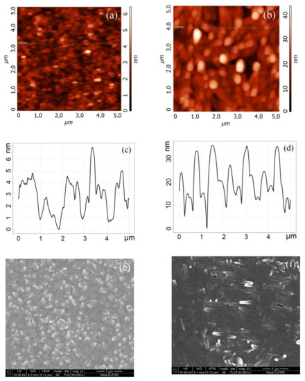
Figure 1.
Vanadium oxide film surface formed at 10,000 pulse number (a,c,e) and at 60,000 pulse number (b,d,f): (a,b)—AFM-images; (c,d)—AFM cross-section; (e,f)—SEM-image.
To experimentally study the effect of the pulse number on the morphological and electrophysical parameters of vanadium oxide films, 6 samples were fabricated on TiN/Si structure under the following conditions: substrate temperature 800 °C, laser frequency 10 Hz, oxygen pressure 3 × 10⁻⁴ Torr. The samples were made with a different number of pulses in the range from 10,000 to 60,000 with a step of 10,000 pulses. Based on the obtained experimental results, the dependences of geometric (film thickness, surface roughness) parameters on the pulse number (Figure 2) and electrophysical (electron concentration, electron mobility, resistivity) on film thickness (Figure 3) were established.
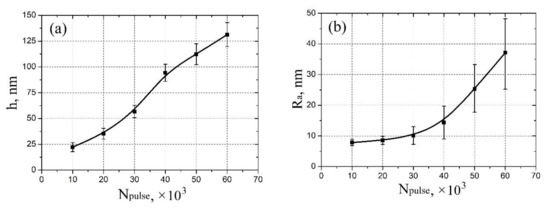
Figure 2.
Experimental study of vanadium oxide film geometrical parameters dependence on pulse number: (a)—thickness; (b)—surface roughness.
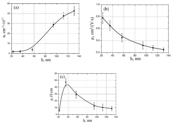
Figure 3.
Experimental study electrophysical parameters dependence on vanadium oxide film thickness: (a)—electron concentration; (b)—electron mobility; (c)—resistivity.
To experimentally study the effect of oxygen pressure on the morphological and electrophysical parameters of vanadium oxide films, five samples were prepared on TiN/Si structure under the following modes: substrate temperature 800 °C, laser frequency 10 Hz, number of pulses: 10,000. The samples were made at different oxygen pressures: 3 × 10⁻⁴ Torr, 1 × 10⁻³ Torr, 2 × 10⁻³ Torr, 1 × 10⁻² Torr, and 3 × 10⁻² Torr. Based on the obtained experimental results, the dependences of geometric (film thickness, surface roughness) (Figure 4) and electrophysical (electron concentration, electron mobility, resistivity) parameters on oxygen pressure (Figure 5) were established.
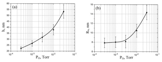
Figure 4.
Experimental study of vanadium oxide film geometrical parameters dependence on oxygen pressure: (a)—thickness; (b)—surface roughness.
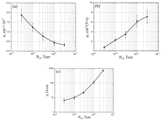
Figure 5.
Experimental study of vanadium oxide film electrophysical parameters dependence on oxygen pressure: (a)—electron concentration; (b)—electron mobility; (c)—resistivity.
Geometric parameters of the vanadium oxide films were studied by atomic force microscopy (AFM) in the semicontact mode using the Ntegra Probe Nanolaboratory (NT-MDT, Zelenograd, Russia) and a commercial cantilever NSG11 with 255 kHz resonant frequency and 11.8 N/m spring constant. Vanadium oxide film thickness was determined using AFM by scanning of (vanadium oxide)/TiN interface. Processing of the results was carried out using the «Image Analysis 2.0» software package. Vanadium oxide film structure was investigated using Nova NanoLab 600 raster electron microscope (FEI Company, Hillsboro, OR, USA).
The electrophysical parameters of vanadium oxide films were studied using an Ecopia HMS-3000 Hall effect system (Ecopia Co., Anyang, Korea).
The resistive switching effect in vanadium oxide films was studied using a Keithley 4200-SCS semiconductor parameter analyzer (Keithley Instruments, Solon, OH, USA) and an EM-6070A submicron probe system (Planar, Republic of Belarus). TiN bottom electrode (BE) was grounded, W probe with diameter about 100 nm was used as the top electrode (TE). The compliance current was set to 0.7 mA to avoid thermal breakdown of vanadium oxide films. As a result, current-voltage (I-V) curves were obtained in the sweep voltage range from −3 V to 3 V for samples with a thickness of 22.3 ± 4.4 nm and 131.7 ± 14.4 nm at different points on the surface of the vanadium oxide film (Figure 6). Based on TE experimental results, the uniformity test (study of resistance switching at one point on the surface of a vanadium oxide film) and homogeneity test (study of resistance switching at different points on the surface of a vanadium oxide film) were carried out (Figure 7).
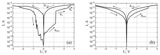
Figure 6.
I-V characteristics of vanadium oxide films with different film thickness: (a)—22.3 ± 4.4 nm; (b)—131.7 ± 14.4 nm.
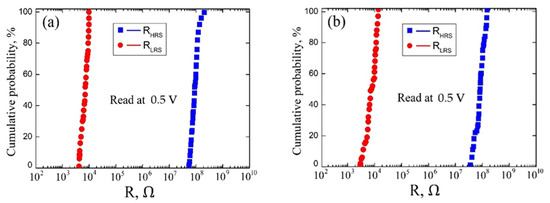
Figure 7.
Cumulative probability data for the resistances of RHRS and RLRS for vanadium oxide films with 22.3 ± 4.4 nm film thickness: (a)—uniformity test; (b)—homogeneity test.
3. Results and Discussion
Figure 1 shows the results of experimental studies of the morphology of a vanadium oxide film with thicknesses 22.3 ± 4.4 nm and 131.7 ± 14.4 nm. It is shown that a film with a thickness of 22.3 ± 4.4 nm (10,000 pulse number) is granular (Figure 1e), when a film with a thickness of 131.7 ± 14.4 nm (60,000 pulse number) (Figure 2f) has a nanorod structure on the surface. This result can be explained by the dominance of different mechanisms of thin film growth with increasing vanadium oxide film thickness during the pulsed laser deposition process [54].
Based on the obtained experimental results, the dependences of the thickness and surface roughness of vanadium oxide films on the pulse number were established (Figure 2). It was shown that an increase in the pulse number from 10,000 to 60,000 leads to an increase in the thickness from 22.3 ± 4.4 nm to 131.7 ± 14.4 nm (Figure 2a), and to an increase in the surface roughness from 7.8 ± 1.1 nm to 37.1 ± 11.2 nm (Figure 2b). It should be noted that an increase in the pulse number may lead to a gradual transition of the vanadium oxide film from a granular structure to nanorod structure. One can assume that the possible mechanism for this phenomenon consists of two-stage process [54]. At the first stage, high-density crystalline nuclei are grown on the substrate surface, forming a granular film; at the second stage, due to the high surface energy of the substrate plane, the growth of the vanadium oxide film in one of the directions dominate, as a result nanorods are formed.
Figure 3 shows the results of experimental studies of thickness influence on the electrophysical properties of vanadium oxide films. It was shown that an increase in the thickness from 22.3 ± 4.4 nm to 131.7 ± 14.4 nm leads to an increase in the electron concentration of vanadium oxide from (1.87 ± 0.32) × 1017 cm−3 to (42.64 ± 4.46) × 1017 cm−3 (Figure 3a) and a decrease in the mobility of electrons from 0.78 ± 0.09 cm2/(V·s) to 0.25 ± 0.03 cm2/(V·s) (Figure 3b). This result can be explained by the fact that an increase in the pulse number and, therefore, in the thickness of the vanadium oxide film, leads to a decrease in the grain diameter [55]. This leads to an increase in grain density and the area of grain boundaries, which are defects with destroyed V-O bonds (oxygen vacancies) and has an additional number of electrons [56]. Therefore, we observe an increase in the electron concentration with an increase in the pulse number. A decrease in the mobility of electrons with an increase in the pulse number can also be explained by an increase in grain boundaries, which are an additional potential barrier for electrons. In addition, the analysis of the obtained results showed that an increase in the thickness of the vanadium oxide film from 22.3 ± 4.4 nm to 35.23 ± 5.26 nm leads to an increase in the resistivity from 6.32 ± 2.21 Ω·cm to 47.32 ± 6.32 Ω·cm. A further increase in the vanadium oxide film thickness from 35.23 ± 5.26 nm to 131.32 ± 11.64 nm leads to a decrease in the resistivity from 47.32 ± 6.32 Ω·cm to 8.74 ± 3.43 Ω·cm (Figure 3c).
This result can be explained also by the dominance of different growth mechanisms with different film thickness. The grain diameter has a complex dependence on the thickness, so with an increase in the thickness of the vanadium oxide film to about 40 nm, a decrease in the grain diameter of the granular film is observed, and a further increase in the thickness leads to an increase in the grain diameter with the formation of nanorods [54]. Energies of particles in the laser plume are different, and when hitting the substrate, these particles can interact with each other in different ways, with the formation of grains of different sizes. It is important to note that changes in the size of grains are associated not only with an increase or decrease in their area, but also with a change in their shape and location relative to each other. It can be assumed that the maximum value of the resistivity (Figure 3c) corresponds to the maximum area of grain boundaries, with different content of defects, charge carriers, and, therefore, resistance. It can be assumed that an increase in the resistivity from 6.32 ± 2.21 Ω·cm to 47.32 ± 6.32 Ω·cm with an increase in the film thickness from 22.32 ± 4.43 nm to 35.23 ± 5.26 nm is associated with a significant contribution of bulk conduction to the total conduction, along with grain-boundary conduction [57]. In this case, an increase in the volume fraction of a grain and an increase in the distance of overcoming the charge carriers between the grain boundaries can lead to an increase in the resistivity of the vanadium oxide film. A decrease in the resistivity from 47.32 ± 6.32 Ω·cm to 8.74 ± 3.43 Ω·cm with an increase in the film thickness from 35.23 ± 5.26 nm to 131.32 ± 11.64 nm can be associated with a change in the morphology of the film from granular structure to nanorod structure and dominance of rod boundary conduction over bulk conduction.
Analysis of the experimental results of studying the influence of oxygen pressure on geometric parameters showed that an increase in oxygen pressure from 3 × 10⁻⁴ Torr to 3 × 10⁻² Torr leads to an increase in the film thickness from 22.32 ± 1.43 nm to 53.32 ± 5.65 nm (Figure 4a) and an increase in surface roughness from 7.8 ± 1.1 nm to 14.3 ± 1.5 nm (Figure 4b). This result can be explained by an increase in the number of oxygen atoms with increasing pressure, which leads to an increase in the formation of the number of V-O bonds with the formation of vanadium oxide atoms, and, finally, to an increase in the film thickness and surface roughness [54]. Detailed description of phase composition and stoichiometry of vanadium oxide obtained by pulsed laser deposited are presented in [58].
Figure 5 shows the results of experimental studies of oxygen pressure on the electrophysical properties of vanadium oxide films. It was shown that an increase in the oxygen pressure from 3 × 10⁻⁴ Torr to 3 × 10⁻² Torr leads to a decrease in the electron concentration of vanadium oxide from (1.87 ± 0.32) × 1017 cm−3 to (0.32 ± 0.07) × 1017 cm−3 (Figure 5a), an increase in the electron mobility from 0.78 ± 0.09 cm2/(V·s) to 7.12 ± 1.32 cm2/(V·s) (Figure 5b), and an increase in the resistivity from 6.32 ± 2.21 Ω·cm to 723.74 ± 89.21 Ω·cm (Figure 5c). This result can be explained by the fact that the concentration of electrons in the vanadium oxide film is directly proportional to the concentration of vanadium atoms, which, in turn, is inversely proportional to the oxygen pressure. This assumption is confirmed by the value of the resistivity of the films obtained at low (less than 0.003 Torr) oxygen pressures, which are comparable to the resistivity of metals. In addition, at different oxygen pressures, the formation of oxide phases with different stoichiometric ratios of vanadium and oxygen is possible. The combination of these phases also affects the electrical properties of vanadium oxide films. Therefore, an increase in the oxygen pressure leads to an increase in phases with a high oxygen content (V2O3, V2O5), which, in turn, leads to a decrease in the electron mobility and an increase in the resistivity of the vanadium oxide film with an increase in the oxygen pressure.
The effect of resistive switching was studied on two films with different structures: granular and nanorod. For the granular structure films, a film with a thickness of 22.3 ± 4.4 nm was chosen, since it has the lowest roughness and resistivity, which is important for fabricating ReRAM neuromorphic structures with low energy consumption and a high degree of element integration. A film with a thickness of 131.7 ± 14.4 nm with the lowest resistivity was also selected from the nanorod structure films.
An analysis of the results obtained for studying the effect of resistive switching showed that a film with a thickness of 22.3 ± 4.4 nm exhibits a bipolar effect of resistive switching and has 4 regions: RHRS at voltages from 0 V to 1.2 ± 0.1 V, R2 at voltages from 1.2 ± 0.1 V to 2.3 ± 0.1 V, R3 at voltages from 2.3 ± 0.1 V to 2.6 ± 0.1 V and RLRS at voltages above 2.6 ± 0.1 V. The RHRS was (89.42 ± 32.37) × 106 Ω at 0.5 V read voltage, R2 was (32.53 ± 12.73) × 103 Ω at 1.5 V read voltage, R3 was (8.47 ± 1.34) × 103 Ω at 2.5 V read voltage V, RLRS was equal to (6.34 ± 2.34) × 103 Ω with a read voltage of 0.5 V. The ratio RHRS/RLRS was about 14,104. This result can be associated with the phase inhomogeneity of the vanadium oxide film over the thickness. If we assume that in the process of PLD, with an increase in the pulse number, an increase in the number of oxygen atoms interacting with vanadium atoms occurs, this increase in the deposition time leads to the formation of oxides of higher order. As a result, the vanadium oxide film consists of several phases with different values of electrophysical parameters. In this case, the resistivity of the vanadium oxide film increases from the VO phase to the V2O5 phase (from the lower contact (BE) to the upper contact (TE)). This leads to the fact that the activation energy of oxygen atoms for the formation of a pair of O−2 (oxygen ions) and VO (oxygen vacancy) also increases when moving from the film region with the VO phase to the film region with the V2O5 phase. Thus, to generate an oxygen vacancy in each phase, it is required to apply an external electric field above a certain value, which will impart energy to oxygen atoms above the activation energy. Based on this, it can be assumed that the RHRS for the I–V characteristic in Figure 6a corresponds to the situation when oxygen vacancies are concentrated near the bottom contact in the VO phase. At a voltage of 1.2 ± 0.1 V, oxygen vacancies are formed in the VO2 phase and IV curve goes to the R2 region. At a voltage of 2.3 ± 0.1 V, the oxygen atoms receive sufficient energy to form a pair of O−2 and VO in the V2O3 phase, IV curve goes to the R3 region. At a voltage of 2.6 ± 0.1 V, the oxygen vacancies reach the upper contact and the film transforms into the RLRS state. It can also be seen from the analysis of the I–V characteristics that at negative voltages, no plateaus are observed on the curve, as at positive ones. This may be due to the features of resistive switching from the RHRS state to the RLRS, in particular, with the dominance of the temperature gradient over the electric field gradient and the concentration gradient of oxygen vacancies, which leads to the excessive release of Joule heat in the film volume and destruction of the entire nanoscale conduction channel, rather than its separate section [58].
In addition, an analysis of the obtained results of studying the resistive switching showed that a film with a thickness of 131.7 ± 14.4 nm exhibits a bipolar effect of resistive switching and has 2 resistive states: at a voltage of 2.3 ± 0.2 V, the film switched from the RHRS state to RLRS, and at a voltage of −2.8 ± 0.1 the film was switched back to the RHRS state (Figure 6b). The resistances of the RHRS and RLRS were (50.72 ± 13.42) × 103 Ω and (12.34 ± 3.75) × 103 Ω at a reading voltage of 1.0 V, respectively. The ratio RHRS/RLRS was about 4. Analysis of the literature data showed that the main mechanism of conduction in oxide nanorods is the correlated barrier hopping model, according to which current transfer occurs due to the hopping of charge carriers between defects over a potential barrier separating them [59,60,61].
An analysis of the experimental results of studying the uniformity of resistive switching in a vanadium oxide film with a thickness of 22.3 ± 4.4 nm showed that RLRS varied in the range from 4.27 × 10³ Ω to 9.88 × 10³ Ω, and RHRS varied in the range from 5.32 × 10⁷ Ω to 1.23 × 10⁸ Ω. The mean values RLRS = (6.34 ± 2.34) × 103 Ω and RHRS = (89.42 ± 32.37) × 106 Ω corresponded to the probabilities of 41% and 52%, respectively (Figure 7a). An analysis of the experimental results of studying the homogeneity of resistive switching in a vanadium oxide film with a thickness of 131.7 ± 14.4 nm showed that RLRS varied in the range from 2.93 × 10³ Ω to 1.37 × 10⁴ Ω, and RHRS varied in the range from 3.64 × 10⁷ Ω to 1.51 × 10⁸ Ω. The mean values RLRS = (6.34 ± 2.34) × 103 Ω and RHRS = (89.42 ± 32.37) × 106 Ω corresponded to the probabilities of 37% and 61%, respectively (Figure 7b).
The different range of RHRS and RLRS values for uniformity and homogeneity can be explained by different values of the vanadium oxide film thickness, as well as different concentrations and distribution profiles of oxygen vacancies in the volume at different points on the vanadium oxide surface.
4. Conclusions
The paper presents the results of experimental studies of the influence of the PLD control parameters on the morphological and electrophysical parameters of vanadium oxide films. It is shown that an increase in the pulse number from 10,000 to 60,000 leads to an increase in the thickness of the vanadium oxide film from 22.3 ± 4.4 nm to 131.7 ± 14.4 nm, surface roughness from 7.8 ± 1.1 nm to 37.1 ± 11.2 nm, and electron concentration from (1.87 ± 0.32) × 1017 cm−3 to (42.64 ± 4.46) × 1017 cm−3, and a decrease in the electron mobility from 0.78 ± 0.09 cm2/(V·s) to 0.25 ± 0.03 cm2/(V·s). It is shown that an increase in the film thickness from 22.3 ± 4.4 nm to 35.23 ± 5.26 nm leads to an increase in the resistivity from 6.32 ± 2.21 Ω·cm to 47.32 ± 6.32 Ω·cm, and an increase in the film thickness from 35.23 ± 5.26 nm to 131.32 ± 11.64 nm leads to a decrease in the specific resistance from 47.32 ± 6.32 Ω·cm to 8.74 ± 3.43 Ω·cm. This result can be explained by the predominance of different growth mechanisms on samples with different film thicknesses of vanadium oxide, which leads to the formation of films with different structures.
An analysis of the obtained experimental results showed that an increase in the oxygen pressure from 3 × 10⁻⁴ Torr to 3 × 10⁻² Torr leads to an increase in the thickness of the vanadium oxide film from 22.32 ± 1.43 nm to 53.32 ± 5.65 nm, and the surface roughness from 7.8 ± 1.1 nm to 14.3 ± 1.5 nm, electron mobility from 0.78 ± 0.09 cm2/(V·s) to 7.12 ± 1.32 cm2/(V·s), resistivity from 6.32 ± 2.21 Ω·cm to 723.74 ± 89.21 Ω·cm, and a decrease in concentration electrons from (1.87 ± 0.32) × 1017 cm−3 to (0.32 ± 0.07) × 1017 cm−3. This result can be explained by the formation of oxide phases with different stoichiometric ratios of vanadium and oxygen at different oxygen pressures.
An analysis of the obtained experimental results of studying the effect of resistive switching showed that a vanadium oxide film 22.3 ± 4.4 nm thick exhibits a bipolar effect of resistive switching and has 4 different resistive states. The RHRS was (89.42 ± 32.37) × 106 Ω at 0.5 V read voltage, R2 was (32.53 ± 12.73) × 103 Ω at 1.5 V read voltage, R3 was (8.47 ± 1.34) × 103 Ω at 2.5 V read voltage V, RLRS was equal to (6.34 ± 2.34) × 103 Ω with a read voltage of 0.5 V. The ratio RHRS/RLRS was about 14,104. This result can also be associated with the phase inhomogeneity of the vanadium oxide film over the thickness. As a result, in different parts of the oxide film volume, the activation energy of oxygen atoms for the formation of a pair O−2 and VO has different values. Therefore, imparting additional energy to atoms by increasing the sweep voltage amplitude leads to a sharp generation of oxygen vacancies in a particular phase and a sharp change in the resistance of the oxide film. At a voltage of 1.2 ± 0.1 V, oxygen vacancies are formed in the VO2 phase and the vanadium oxide film transforms into the R2 state. At a voltage of 2.3 ± 0.1 V, the oxygen atoms receive sufficient energy to form a pair of O−2 and VO in the V2O3 phase, and the vanadium oxide film transforms into the R3 state. At a voltage of 2.6 ± 0.1 V, the oxygen vacancies reach the upper contact and the film transforms into the RLRS state.
Moreover, an analysis of the obtained results of studying the resistive switching showed that a film with a thickness of 131.7 ± 14.4 nm exhibits a bipolar effect of resistive switching and has two resistive states: RHRS = (50.72 ± 13.42) × 103 Ω and RLRS = (12.34 ± 3.75) × 103 Ω at a reading voltage of 1.0 V. The probable mechanism of resistive switching in the film with a nanorod structure can be described by the correlated barrier hopping model.
An analysis of the experimental results of studying the resistive switching in a vanadium oxide film with a thickness of 22.3 ± 4.4 nm showed that RLRS varied in the range from 4.27 × 10³ Ω to 9.88 × 10³ Ω, and RHRS varied in the range from 5.32 × 10⁷ Ω to 1.23 × 10⁸ Ω for uniformity test; RLRS varied in the range from 2.93 × 10³ Ω to 1.37 × 10⁴ Ω, and RHRS varied in the range from 3.64 × 10⁷ Ω to 1.51 × 10⁸ Ω for homogeneity test.
The results can be used in the manufacture of new-generation micro- and nanoelectronics elements to create ReRAM elements of neuromorphic systems based on vanadium oxide thin films.
Author Contributions
Conceptualization and validation, O.A.A. and V.A.S.; methodology, V.A.S., R.V.T.; investigation, R.V.T., V.I.A. and N.V.P.; writing—Original draft preparation, R.V.T. and V.A.S.; data curation and formal analysis, V.I.A., D.A.K.; visualization R.V.T. and Z.E.V.; vanadium oxide films growth Z.E.V.; supervision, V.A.S.; project administration, writing—Review and editing, O.A.A. All authors contributed to the writing of the manuscript, which was coordinated by O.A.A. and V.A.S. All authors have read and agreed to the published version of the manuscript.
Funding
The research was supported by the Ministry of Science and Higher Education of the Russian Federation; the state task in the field of scientific activity No. 0852-2020-0015.
Institutional Review Board Statement
Not applicable.
Informed Consent Statement
Not applicable.
Data Availability Statement
Not applicable.
Acknowledgments
The results were obtained using the equipment of the Research and Education Center “Nanotechnologies” at the Southern Federal University.
Conflicts of Interest
The authors declare no conflict of interest.
References
- Kriegeskorte, N. Deep neural networks: A new framework for modeling biological vision and brain information processing. Annu. Rev. Vis. Sci. 2015, 1, 417–446. [Google Scholar] [CrossRef] [PubMed]
- Spoerer, C.J.; McClure, P.; Kriegeskorte, N. Recurrent convolutional neural networks: A better model of biological object recognition. Front. Psychol. 2017, 8, 1551. [Google Scholar] [CrossRef] [PubMed]
- Cichy, R.M.; Kaiser, D. Deep neural networks as scientific models. Trends Cogn. Sci. 2019, 23, 305–317. [Google Scholar] [CrossRef] [PubMed]
- Hasson, U.; Nastase, S.A.; Goldstein, A. Direct fit to nature: An evolutionary perspective on biological and artificial neural networks. Neuron 2020, 105, 416–434. [Google Scholar] [CrossRef]
- Bornholdt, S.; Graudenz, D. General asymmetric neural networks and structure design by genetic algorithms. Neural Netw. 1992, 5, 327–334. [Google Scholar] [CrossRef]
- Lu, C.H.; Lin, C.S.; Chao, H.L.; Shen, J.S.; Hsiung, P.A. Reconfigurable multi-core architecture-a plausible solution to the von Neumann performance bottleneck. Int. J. Adapt. Innov. Syst. 2015, 2, 217–231. [Google Scholar] [CrossRef]
- Zanotti, T.; Puglisi, F.M.; Pavan, P. Smart logic-in-memory architecture for low-power non-von neumann computing. IEEE J. Electron. Devices Soc. 2020, 8, 757–764. [Google Scholar] [CrossRef]
- Wright, C.D.; Hosseini, P.; Diosdado, J.A.V. Beyond von-Neumann computing with nanoscale phase-change memory devices. Adv. Funct. Mater. 2013, 23, 2248–2254. [Google Scholar] [CrossRef]
- Tominov, R.V.; Vakulov, Z.E.; Avilov, V.I.; Khakhulin, D.A.; Fedotov, A.A.; Zamburg, E.G.; Ageev, O.A. Synthesis and Memristor Effect of a Forming-Free ZnO Nanocrystalline Films. Nanomaterials 2020, 10, 1007. [Google Scholar] [CrossRef]
- Jain, A.; Srikanth, S.; DeBenedictis, E.P.; Krishna, T. Merge network for a non-von Neumann accumulate accelerator in a 3D chip. In Proceedings of the 2018 IEEE International Conference on Rebooting Computing (ICRC), McLean, VA, USA, 7–9 November 2018; Volume 1, pp. 1–11. [Google Scholar]
- Jo, S.H.; Chang, T.; Ebong, I.; Bhadviya, B.B.; Mazumder, P.; Lu, W. Nanoscale memristor device as synapse in neuromorphic systems. Nano Lett. 2010, 10, 1297–1301. [Google Scholar] [CrossRef]
- Indiveri, G.; Liu, S.C. Memory and information processing in neuromorphic systems. Proc. IEEE 2015, 103, 1379–1397. [Google Scholar] [CrossRef]
- Hu, M.; Li, H.; Chen, Y.; Wu, Q.; Rose, G.S.; Linderman, R.W. Memristor crossbar-based neuromorphic computing system: A case study. IEEE Trans. Neural Netw. Learn. Syst. 2014, 25, 1864–1878. [Google Scholar] [CrossRef] [PubMed]
- Ambrogio, S.; Balatti, S.; Milo, V.; Carboni, R.; Wang, Z.Q.; Calderoni, A.; Ielmini, D. Neuromorphic learning and recognition with one-transistor-one-resistor synapses and bistable metal oxide RRAM. IEEE Trans. Electron. Devices 2016, 63, 1508–1515. [Google Scholar] [CrossRef]
- Chu, M.; Kim, B.; Park, S.; Hwang, H.; Jeon, M.; Lee, B.H.; Lee, B.G. Neuromorphic hardware system for visual pattern recognition with memristor array and CMOS neuron. IEEE Trans. Ind. Electron. 2014, 62, 2410–2419. [Google Scholar] [CrossRef]
- Ren, Y.; Milo, V.; Wang, Z.; Xu, H.; Ielmini, D.; Zhao, X.; Liu, Y. Analytical modeling of organic–inorganic CH3NH3PbI3 Perovskite resistive switching and its application for Neuromorphic recognition. Adv. Theory Simul. 2018, 1, 1700035. [Google Scholar] [CrossRef]
- Avilov, V.; Polupanov, N.; Tominov, R.; Solodovnik, M.; Konoplev, B.; Smirnov, V.; Ageev, O. Resistive Switching of GaAs Oxide Nanostructures. Materials 2020, 13, 3451. [Google Scholar] [CrossRef]
- Diehl, P.U.; Pedroni, B.U.; Cassidy, A.; Merolla, P.; Neftci, E.; Zarrella, G. Truehappiness: Neuromorphic emotion recognition on truenorth. In Proceedings of the 2016 International Joint Conference on Neural Networks (IJCNN), Vancouver, BC, Canada, 24–29 July 2016; Volume 1, pp. 4278–4285. [Google Scholar]
- Sun, S.; Li, J.; Li, Z.; Liu, H.; Li, Q.; Xu, H. Low-consumption neuromorphic memristor architecture based on convolutional neural networks. In Proceedings of the 2018 International Joint Conference on Neural Networks (IJCNN), Rio de Janeiro, Brazil, 8–13 July 2018; Volume 1, pp. 1–6. [Google Scholar]
- Avilov, V.I.; Smirnov, V.A.; Tominov, R.V.; Sharapov, N.A.; Avakyan, A.A.; Polyakova, V.V.; Ageev, O.A. Atomic force microscopy of titanium oxide nanostructures with forming-free resistive switching. IOP Conf. Ser. Mater. Sci. Eng. 2019, 699, 012004. [Google Scholar] [CrossRef]
- Boahen, K.A. Communicating neuronal ensembles between neuromorphic chips. In Neuromorphic Systems Engineering; Springer: Boston, MA, USA, 1998; Volume 1, pp. 229–259. [Google Scholar]
- Smirnov, V.A.; Tominov, R.V.; Avilov, V.I.; Avakyan, A.A.; Ageev, O.A. Forming-free resistive switching in nanocrystalline HfO2 films. IOP Conf. Ser. Mater. Sci. Eng. 2019, 699, 012053. [Google Scholar] [CrossRef]
- Ageev, O.; Konoplev, B. Nanotechnology in Microelectronics, 1st ed.; Nauka Publisher: Moscow, Russia, 2019; p. 511. [Google Scholar]
- Klimin, V.S.; Tominov, R.V.; Avilov, V.I.; Dukhan, D.D.; Rezvan, A.A.; Zamburg, E.G.; Ageev, O.A. Nanoscale profiling and memristor effect of ZnO thin films for RRAM and neuromorphic devices application. Int. Soc. Opt. Photonics 2018, 11022, 110220E. [Google Scholar]
- Mikolajick, T.; Dehm, C.; Hartner, W.; Kasko, I.; Kastner, M.J.; Nagel, N.; Mazure, C.N. FeRAM technology for high density applications. Microelectron. Reliab. 2001, 41, 947–950. [Google Scholar] [CrossRef]
- Suzuki, M. Review on Future Ferroelectric Nonvolatile Memory: FeRAM. J. Ceram. Soc. Jpn. 1995, 103, 1099–1111. [Google Scholar] [CrossRef][Green Version]
- Engel, B.N.; Akerman, J.; Butcher, B.; Dave, R.W.; DeHerrera, M.; Durlam, M.; Slaughter, J.M. A 4-Mb toggle MRAM based on a novel bit and switching method. IEEE Trans. Magn. 2005, 41, 132–136. [Google Scholar] [CrossRef]
- Huai, Y. Spin-transfer torque MRAM (STT-MRAM): Challenges and prospects. AAPPS Bull. 2008, 18, 33–40. [Google Scholar]
- Choi, Y.; Song, I.; Park, M.H.; Chung, H.; Chang, S.; Cho, B.; Shin, J. A 20 nm 1.8 V 8 Gb PRAM with 40 MB/s program bandwidth. In Proceedings of the 2012 IEEE International Solid-State Circuits Conference, San Francisco, CA, USA, 19–23 February 2012; Volume 1, pp. 46–48. [Google Scholar]
- Demin, V.A.; Surazhevsky, I.A.; Emelyanov, A.V.; Kashkarov, P.K.; Kovalchuk, M.V. Sneak, discharge, and leakage current issues in a high-dimensional 1T1M memristive crossbar. J. Comput. Electron. 2020, 19, 565–575. [Google Scholar] [CrossRef]
- Khakhulin, D.A.; Vakulov, Z.E.; Smirnov, V.A.; Tominov, R.V.; Yoon, J.G.; Ageev, O.A. Resistive switching in ZnO/ZnO: In nanocomposite. J. Phys. Conf. Ser. 2017, 917, 092008. [Google Scholar] [CrossRef]
- Tominov, R.V.; Zamburg, E.G.; Khakhulin, D.A.; Klimin, V.S.; Smirnov, V.A.; Chu, Y.H.; Ageev, O.A. Investigation of resistive switching of ZnxTiyHfzOi nanocomposite for RRAM elements manufacturing. J. Phys. Conf. Ser. 2017, 917, 032023. [Google Scholar] [CrossRef]
- Smirnov, V.A.; Tominov, R.V.; Avilov, V.I.; Alyabieva, N.I.; Vakulov, Z.E.; Zamburg, E.G.; Ageev, O.A. Investigation into the memristor effect in nanocrystalline ZnO films. Semiconductors 2019, 53, 72–77. [Google Scholar] [CrossRef]
- Mikhaylov, A.; Pimashkin, A.; Pigareva, Y.; Gerasimova, S.; Gryaznov, E.; Shchanikov, S.; Erokhin, V. Neurohybrid Memristive CMOS-Integrated Systems for Biosensors and Neuroprosthetics. Front. Neurosci. 2020, 14, 358. [Google Scholar] [CrossRef]
- Shandyba, N.A.; Panchenko, I.V.; Tominov, R.V.; Smirnov, V.A.; Pelipenko, M.I.; Zamburg, E.G.; Chu, Y.H. Size effect on memristive properties of nanocrystalline ZnO film for resistive synaptic devices. J. Phys. Conf. Ser. 2018, 1124, 081036. [Google Scholar] [CrossRef]
- Waser, R.; Dittmann, R.; Staikov, G.; Szot, K. Redox-based resistive switching memories–nanoionic mechanisms, prospects, and challenges. Adv. Mater. 2009, 21, 2632–2663. [Google Scholar] [CrossRef]
- Wei, Z.; Kanzawa, Y.; Arita, K.; Katoh, Y.; Kawai, K.; Muraoka, S.; Mikawa, T. Highly reliable TaOx ReRAM and direct evidence of redox reaction mechanism. In Proceedings of the 2008 IEEE International Electron Devices Meeting, San Francisco, CA, USA, 15–17 December 2008; Volume 1, pp. 1–4. [Google Scholar]
- Kawahara, A.; Azuma, R.; Ikeda, Y.; Kawai, K.; Katoh, Y.; Hayakawa, Y.; Takagi, T. An 8 Mb multi-layered cross-point ReRAM macro with 443 MB/s write throughput. IEEE J. Solid-State Circuits 2012, 48, 178–185. [Google Scholar] [CrossRef]
- Smirnov, V. Nanolithography by local anodic oxidation of thin titanium film. In Piezoelectrics and Nanomaterials: Fundamentals, Developments and Applications, 1st ed.; Parinov, I., Ed.; Nova Science Publisher: Hauppauge, NY, USA, 2015; Volume 1, pp. 85–103. [Google Scholar]
- Kanao, K.; Arie, T.; Akita, S.; Takei, K. An all-solution-processed tactile memory flexible device integrated with a NiO ReRAM. J. Mater. Chem. C 2016, 4, 9261–9265. [Google Scholar] [CrossRef]
- Tominov, R.V.; Smirnov, V.A.; Avilov, V.I.; Fedotov, A.A.; Klimin, V.S.; Chernenko, N.E. Formation of ZnO memristor structures by scratching probe nanolithography. IOP Conf. Ser. Mater. Sci. Eng. 2018, 443, 012036. [Google Scholar] [CrossRef]
- Torre, C.L.; Fleck, K.; Starschich, S.; Linn, E.; Waser, R.; Menzel, S. Dependence of the SET switching variability on the initial state in HfOx-based ReRAM. Phys. Status Solidi 2016, 213, 316–319. [Google Scholar] [CrossRef]
- Kelly, P.J.; Arnell, R.D. Magnetron sputtering: A review of recent developments and applications. Vacuum 2000, 56, 159–172. [Google Scholar] [CrossRef]
- Groner, M.D.; Fabreguette, F.H.; Elam, J.W.; George, S.M. Low-temperature Al2O3 atomic layer deposition. Chem. Mater. 2004, 16, 639–645. [Google Scholar] [CrossRef]
- Yao, B.D.; Chan, Y.F.; Wang, N. Formation of ZnO nanostructures by a simple way of thermal evaporation. Appl. Phys. Lett. 2002, 81, 757–759. [Google Scholar] [CrossRef]
- Li, Y.L.; Kinloch, I.A.; Windle, A.H. Direct spinning of carbon nanotube fibers from chemical vapor deposition synthesis. Science 2004, 304, 276–278. [Google Scholar] [CrossRef]
- Lowndes, D.H.; Geohegan, D.B.; Puretzky, A.A.; Norton, D.P.; Rouleau, C.M. Synthesis of novel thin-film materials by pulsed laser deposition. Science 1996, 273, 898–903. [Google Scholar] [CrossRef]
- Sun, X.W.; Kwok, H.S. Optical properties of epitaxially grown zinc oxide films on sapphire by pulsed laser deposition. J. Appl. Phys. 1999, 86, 408–411. [Google Scholar] [CrossRef]
- Vakulov, Z.E.; Zamburg, E.G.; Khakhulin, D.A.; Ageev, O.A. Thermal stability of ZnO thin films fabricated by pulsed laser deposition. Mater. Sci. Semicond. Process. 2017, 66, 21–25. [Google Scholar] [CrossRef]
- Huotari, J.; Bjorklund, R.; Lappalainen, J.; Spetz, A.L. Pulsed laser deposited nanostructured vanadium oxide thin films characterized as ammonia sensors. Sens. Actuators B Chem. 2015, 217, 22–29. [Google Scholar] [CrossRef]
- Ramana, C.V.; Smith, R.J.; Hussain, O.M.; Julien, C.M. On the growth mechanism of pulsed-laser deposited vanadium oxide thin films. Mater. Sci. Eng. B 2004, 111, 218–225. [Google Scholar] [CrossRef]
- Vakulov, Z.; Zamburg, E.; Khakhulin, D.; Geldash, A.; Golosov, D.A.; Zavadski, S.M.; Ageev, O.A. Oxygen pressure influence on properties of nanocrystalline LiNbO3 films grown by laser ablation. Nanomaterials 2020, 10, 1371. [Google Scholar] [CrossRef]
- Vakulov, Z.E.; Varzarev, Y.N.; Gusev, E.Y.; Skrylev, A.V.; Panich, A.E.; Miakonkikh, A.V.; Ageev, O.A. Influence of Pulsed Laser Deposition Modes on Properties of Nanocrystalline LiNbO3 Films. Russ. Microelectron. 2019, 48, 59–65. [Google Scholar] [CrossRef]
- Cong, G.W.; Wei, H.Y.; Zhang, P.F.; Peng, W.Q.; Wu, J.J.; Liu, X.L.; Wang, Z.G. One-step growth of ZnO from film to vertically well-aligned nanorods and the morphology-dependent Raman scattering. Appl. Phys. Lett. 2005, 87, 231903. [Google Scholar] [CrossRef]
- Chrisey, D.; Hubler, G. Pulsed Laser Deposition of Thin Films; John Willey & Sons: Hoboken, NJ, USA, 1994; p. 613. [Google Scholar]
- Bersuker, G.; Gilmer, D.C.; Veksler, D.; Kirsch, P.; Vandelli, L.; Padovani, A.; Larcher, L.; McKenna, K.; Shluger, A.; Iglesias, V.; et al. Metal oxide resistive memory switching mechanism based on conductive filament properties. J. Appl. Phys. 2011, 110, 124518. [Google Scholar] [CrossRef]
- Chiu, F.C. A review on conduction mechanisms in dielectric films. Adv. Mater. Sci. Eng. 2014, 2014, 578168. [Google Scholar] [CrossRef]
- Wang, Y.L.; Chen, X.K.; Li, M.C.; Wang, R.; Wu, G.; Yang, J.P.; Han, W.H.; Cao, S.Z.; Zhao, L.C. Phase composition and valence of pulsed laser deposited vanadium oxide thin films at different oxygen pressures. Surf. Coat. Technol. 2007, 201, 5344–5347. [Google Scholar] [CrossRef]
- Yang, J.J.; Strukov, D.B.; Stewart, D.R. Memristive devices for computing. Nat. Nanotechnol. 2013, 8, 13. [Google Scholar] [CrossRef]
- Soosen, S.M.; Chandran, A.; Koshy, J.; George, K.C. Correlated barrier hopping in ZnO nanorods. J. Appl. Phys. 2011, 109, 113702. [Google Scholar] [CrossRef]
- Hayat, K.; Rafiq, M.A.; Durrani, S.K.; Hasan, M.M. Impedance spectroscopy and investigation of conduction mechanism in BaMnO3 nanorods. Phys. B Condens. Matter 2011, 406, 309–314. [Google Scholar] [CrossRef]
Publisher’s Note: MDPI stays neutral with regard to jurisdictional claims in published maps and institutional affiliations. |
© 2020 by the authors. Licensee MDPI, Basel, Switzerland. This article is an open access article distributed under the terms and conditions of the Creative Commons Attribution (CC BY) license (http://creativecommons.org/licenses/by/4.0/).