
Optical Biosensors Based on Silicon-On-Insulator Ring Resonators: A Review


Abstract
:1. Introduction
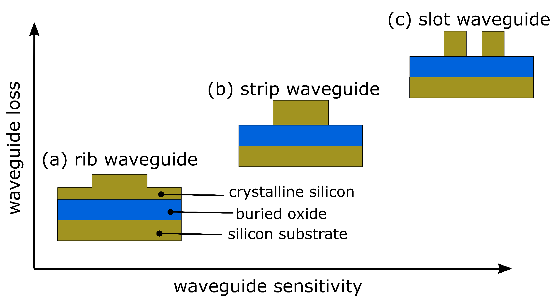
2. Photonic Devices and Sensing Mechanisms
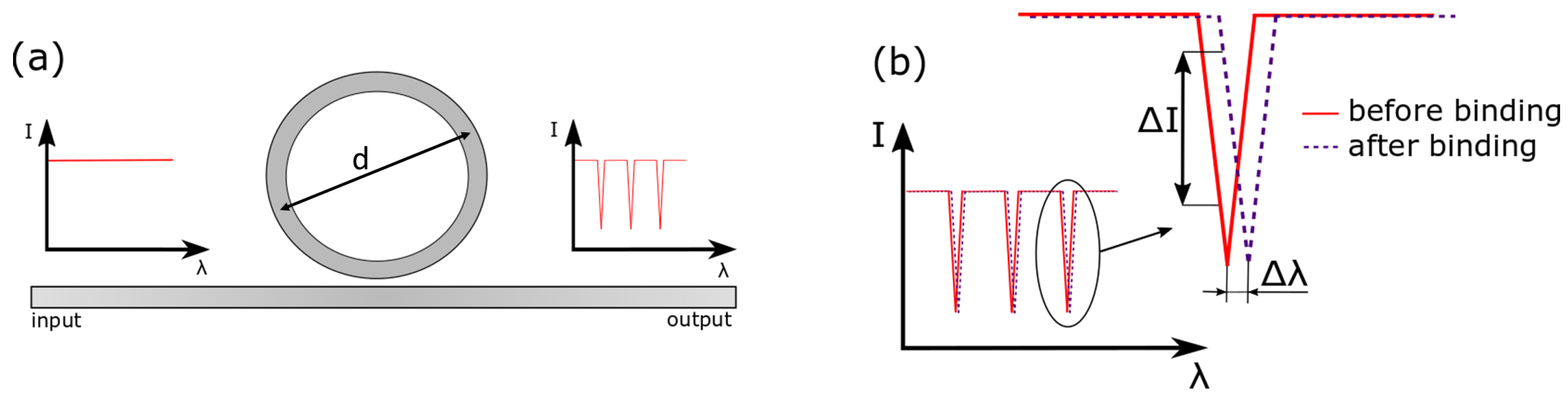
Operation Principle
- Increasing the waveguide sensitivity increases the light-analyte-interaction. In fact, this determines the wavelength shift and has a strong impact on the overall sensitivity.
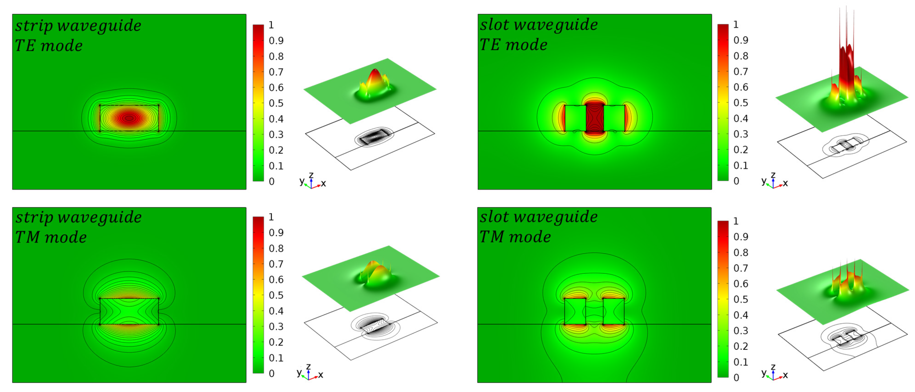
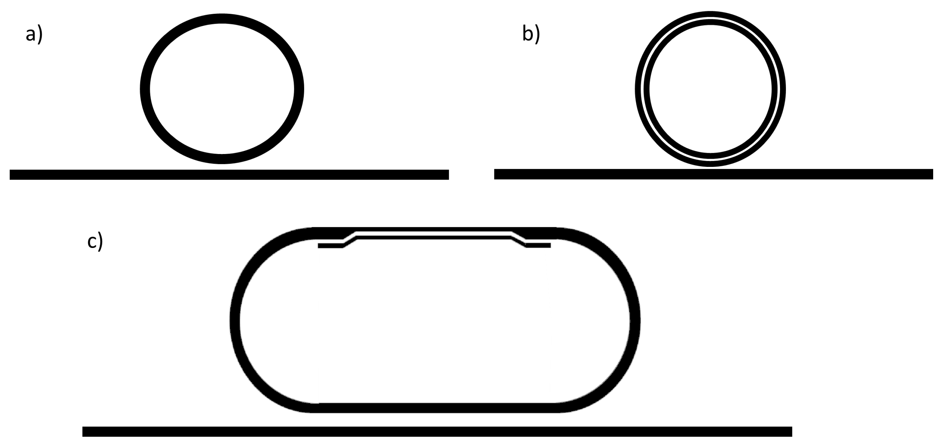
- Enhancing the ring resonator sensitivity , which determines the wavelength shift depending on the refractive index change . This can be achieved by increasing the light-matter interaction using slot waveguide structures.
- A small , i.e., a high Q-factor, impacts the sensitivity of ring resonator sensors since the impact of noise on the determination of the resonance wavelength will be reduced [45,46]. A higher Q-factor leads to a lower attenuation in the ring and minimizes the smallest detectable wavelength shift and consequently the detection limit.
- A small footprint is directly related to the detection time and reduces the area consumption and therefore device costs significantly. Furthermore, this allows a high integration density, which is of special interest for multiplexing.
- Compatibility with a semiconductor production platform, which gives the ability for an industrial production flow. The compatibility with an electronic-photonic integrated circuit (EPIC) allows for a monolithic integration.
3. Functionalization Procedures and Applications
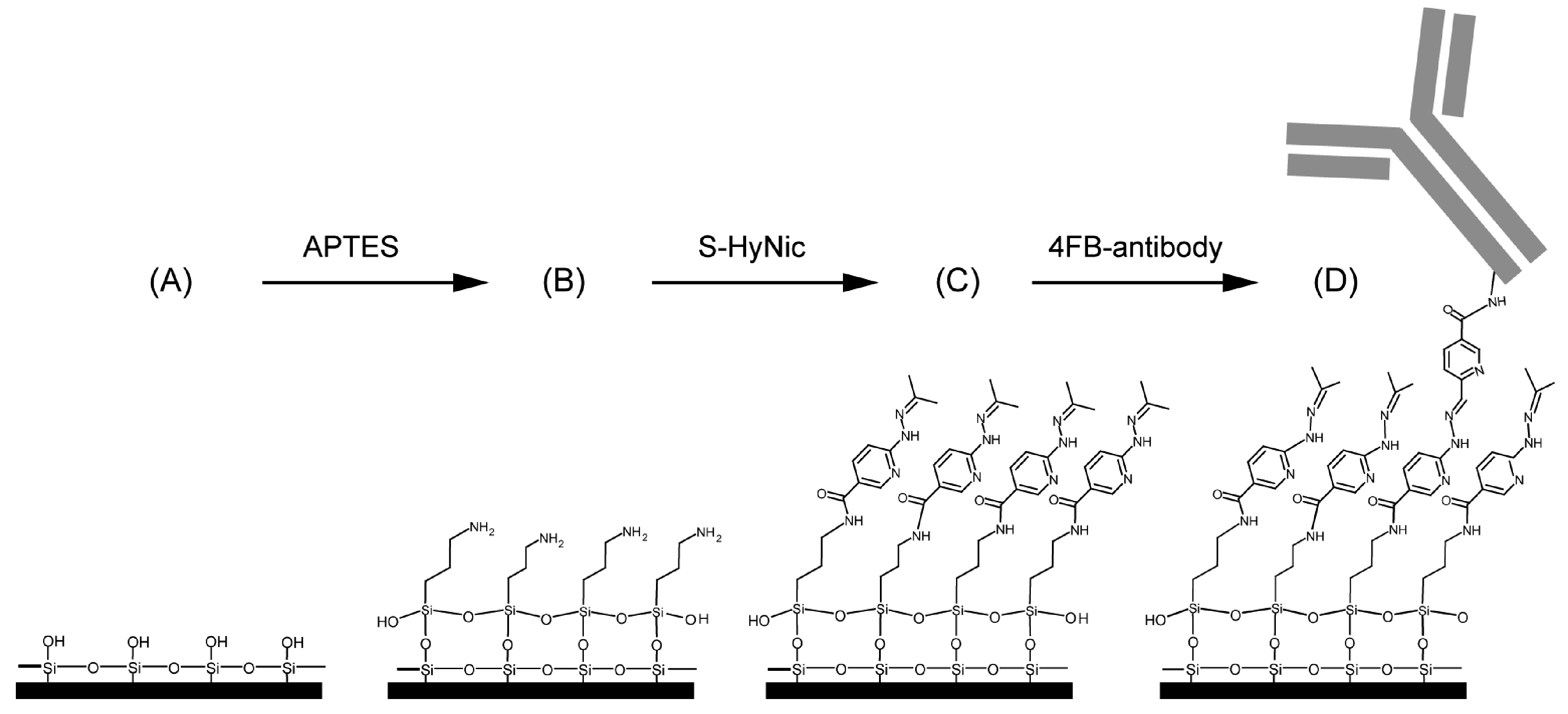
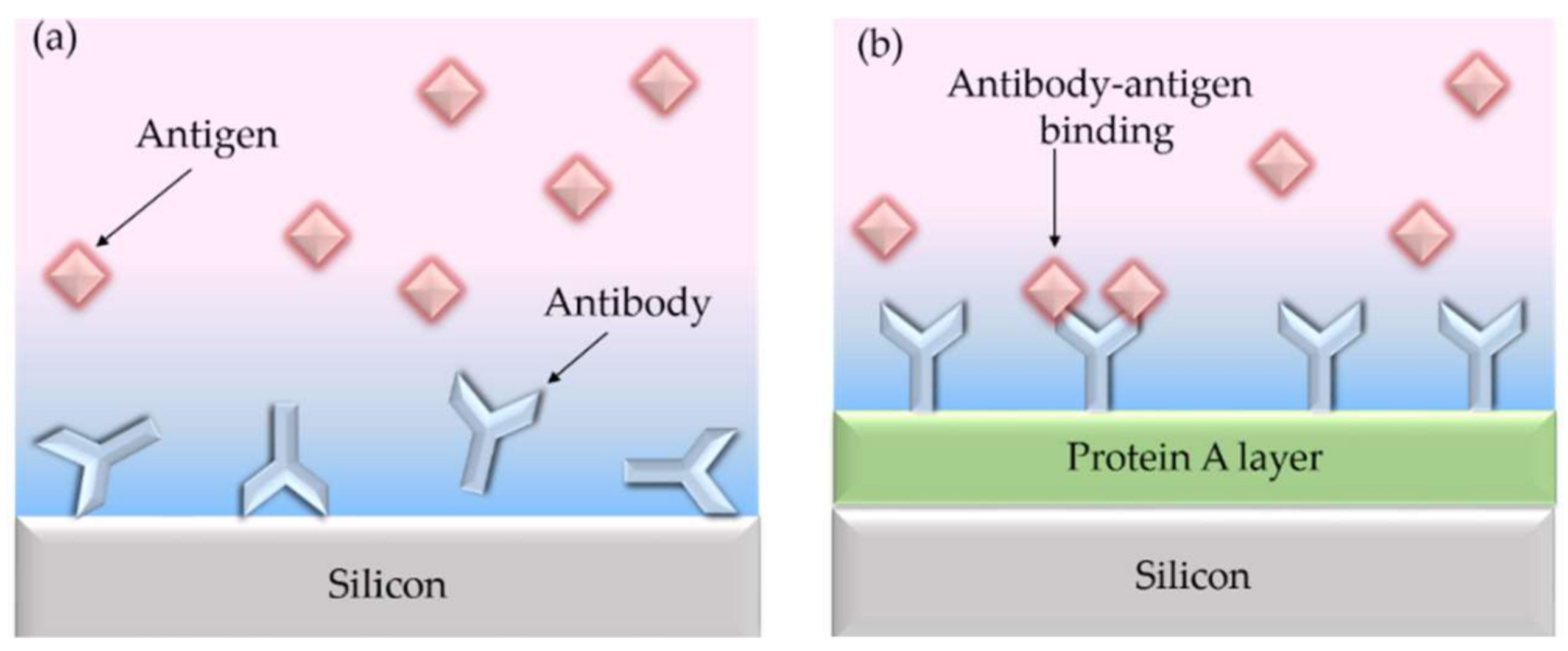
- (A) Surface activationThe surface activation is carried out by cleaning the silicon surface with piranha solution or hydrogen peroxide-ammonium hydroxide solution followed by an argon plasma to generate hydroxyl groups.
- (B) Surface functionalizationTo immobilize the bioactive receptors, agents like bifunctional organosilane of the general formula R-Si-(CH)-X with hydrolysable groups R (OCH, CHCH, Cl, F, SH) are often used, for example, (3-Aminopropyl)triethoxysilane (APTES) (in Figure 5). The choice of functional groups X (NH, epoxy, SH, C=C) depends strongly on the desired specification. The condensation of these materials with the surface hydroxyl groups results in the formation of siloxane bonds (Si-O-Si). Such coupling leads to monolayers that is covalently bonded on the silicon surface and therefore highly stable.
- (C) LinkerThe linker molecules are also bifunctional. In some cases they are symmetrical in structure, such as the widely used amine-to-amine linker glutaraldehyde or bis (sulfosuccinimidyl) suberate (BS3), but may also carry two different functional groups, e.g., N-γ-maleimidobutyryl oxysuccinimide ester (GMBS), which is an amine-to-sulfhydryl crosslinker that contains NHS esters and maleimide reactive groups at opposite ends of a short spacer arm. In the example shown in Figure 5, a heterobifunctional crosslinker reacts with the amino-modified surfaces. In this case, a succinimidyl-6-hydrazino-nicotinamide (S-HyNic) is used as linker molecule.
- (D) Immobilisation of receptorImmobilization of biomolecules as receptors such as antibodies requires a pre-modification of those biomolecules. Thus, biotinylation can introduce functionality into the biomolecule. In the example shown in Figure 5, a 4-formylbenzamide (4FB)-modified antibody is used to form a stable covalent hydrazone linkage at the 6-hydrazinonicotinamide (HyNic) moieties.
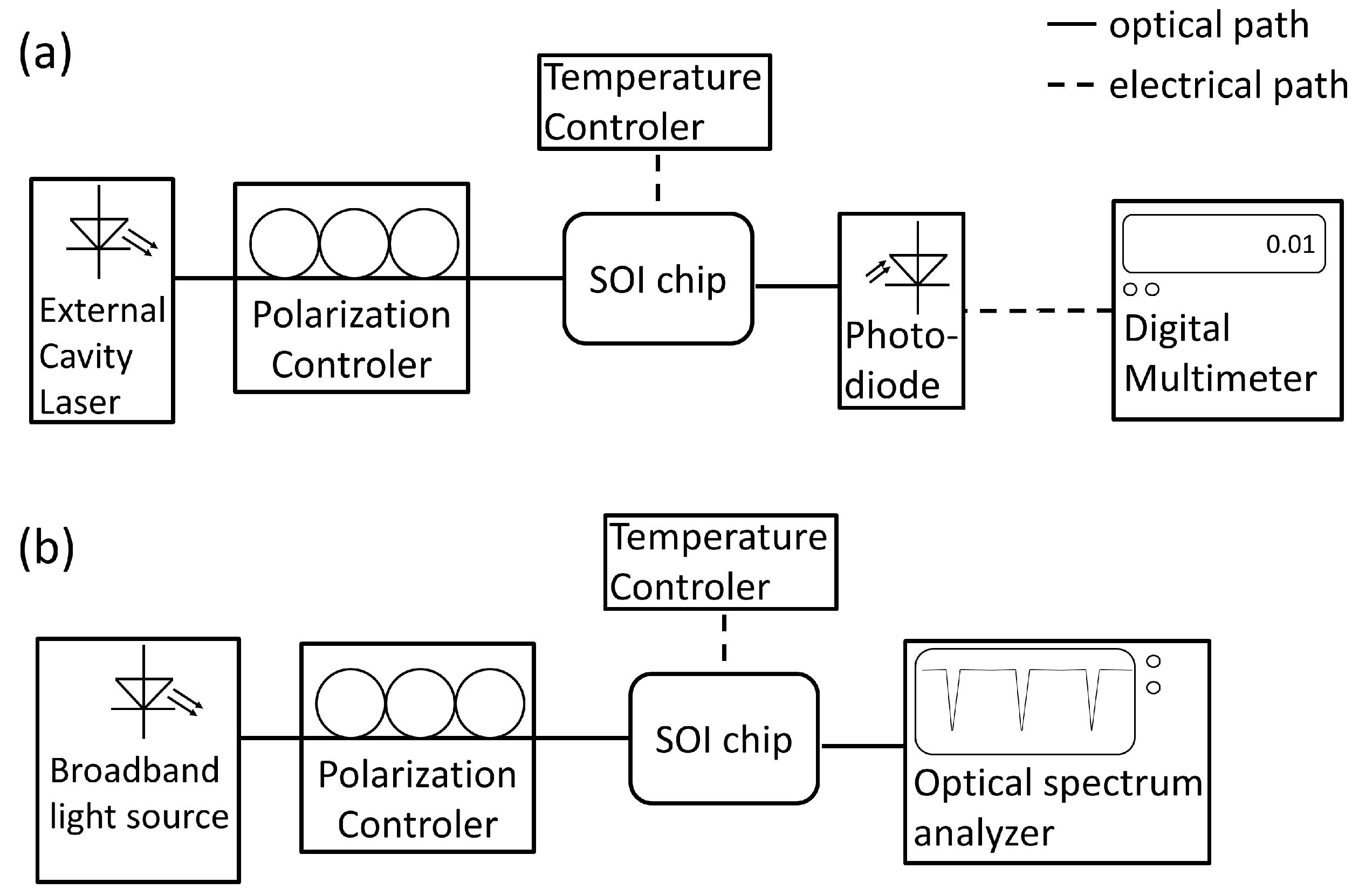
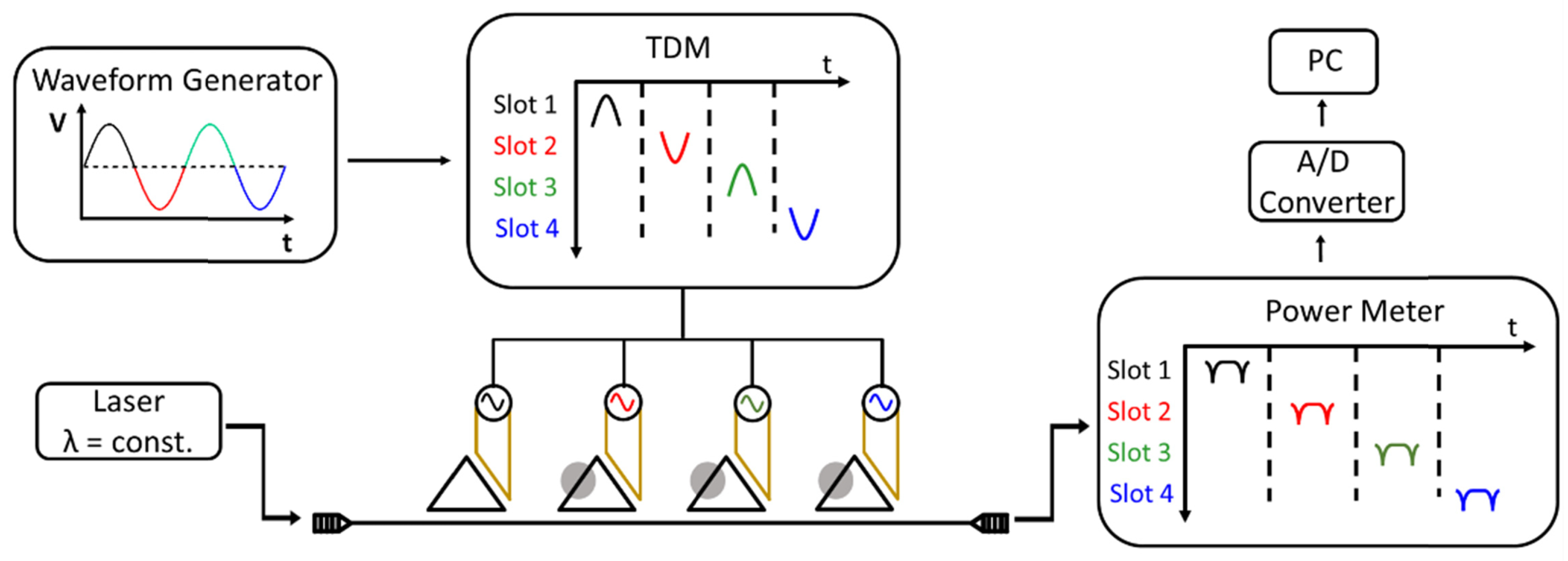
4. System Integration
5. Outlook
6. Conclusions
Author Contributions
Funding
Acknowledgments
Conflicts of Interest
References
- Thomson, D.; Zilkie, A.; Bowers, J.E.; Komljenovic, T.; Reed, G.T.; Vivien, L.; Marris-Morini, D.; Cassan, E.; Virot, L.; Fédéli, J.M.; et al. Roadmap on silicon photonics. J. Opt. 2016, 18, 073003. [Google Scholar] [CrossRef] [Green Version]
- Chrostowski, L.; Hochberg, M. Silicon Photonics Design: From Devices to Systems; Cambridge University Press: Cambridge, UK, 2015. [Google Scholar]
- Boeuf, F.; Cremer, S.; Temporiti, E.; Shaw, M.; Vulliet, N.; Ristoiu, D.; Farcy, A.; Pinguet, T.; Mekis, A.; Masini, G.; et al. Recent progress in silicon photonics R&D and manufacturing on 300 mm wafer platform. In Proceedings of the Optical Fiber Communication Conference, Los Angeles, CA, USA, 22–26 March 2015; p. W3A.1. [Google Scholar]
- Laplatine, L.; Luan, E.; Cheung, K.; Ratner, D.M.; Dattner, Y.; Chrostowski, L. System-level integration of active silicon photonic biosensors using Fan-Out Wafer-Level-Packaging for low cost and multiplexed point-of-care diagnostic testing. Sens. Actuators B Chem. 2018, 273, 1610–1617. [Google Scholar] [CrossRef]
- Knoll, D.; Lischke, S.; Barth, R.; Zimmermann, L.; Heinemann, B.; Rucker, H.; Mai, C.; Kroh, M.; Peczek, A.; Awny, A.; et al. High-performance photonic BiCMOS process for the fabrication of high-bandwidth electronic-photonic integrated circuits. In Proceedings of the 2015 IEEE International Electron Devices Meeting (IEDM), Washington, DC, USA, 7–9 December 2015; pp. 15–16. [Google Scholar]
- Zhou, Z.; Yin, B.; Michel, J. On-chip light sources for silicon photonics. Light Sci. Appl. 2015, 4, e358. [Google Scholar] [CrossRef]
- Sakib, M.N.N.; Sun, J.; Kumar, R.; Driscoll, J.; Rong, H. Demonstration of a 50 Gb/s all-silicon waveguide photodetector for photonic integration. In Proceedings of the CLEO: QELS_Fundamental Science, San Jose, CA, USA, 13–18 May 2018; p. JTh5A.7. [Google Scholar]
- Li, S.; Tarr, G.; Winnie, N.Y. Monolithic integration of SOI waveguide photodetectors and transimpedance amplifiers. In Proceedings of the Silicon Photonics XIII, San Diego, CA, USA, 19–23 August 2018; Volume 10537, p. 105371M. [Google Scholar]
- Alimonti, G.; Ammendola, R.; Andreazza, A.; Badoni, D.; Bonaiuto, V.; Casalboni, M.; Matteis, F.D.; Mai, A.; Paoluzzi, G.; Prosposito, P.; et al. Use of silicon photonics wavelength multiplexing techniques for fast parallel readout in high energy physics. Nucl. Instrum. Methods Phys. Res. Sect. A Accel. Spectrom. Detect. Assoc. Equip. 2018, in press. [Google Scholar] [CrossRef]
- Zang, K.; Zhang, D.; Huo, Y.; Chen, X.; Lu, C.Y.; Fei, E.T.; Kamins, T.I.; Feng, X.; Huang, Y.; Harris, J.S. Microring bio-chemical sensor with integrated low dark current Ge photodetector. Appl. Phys. Lett. 2015, 106, 101111. [Google Scholar] [CrossRef]
- Williams, E.H.; Davydov, A.V.; Motayed, A.; Sundaresan, S.G.; Bocchini, P.; Richter, L.J.; Stan, G.; Steffens, K.; Zangmeister, R.; Schreifels, J.A.; et al. Immobilization of streptavidin on 4H-SiC for biosensor development. Appl. Surf. Sci. 2012, 258, 6056–6063. [Google Scholar] [CrossRef]
- Washburn, A.L.; Luchansky, M.S.; Bowman, A.L.; Bailey, R.C. Quantitative, Label-Free Detection of Five Protein Biomarkers Using Multiplexed Arrays of Silicon Photonic Microring Resonators. Anal. Chem. 2010, 82, 69–72. [Google Scholar] [CrossRef] [Green Version]
- Densmore, A.; Xu, D.X.; Janz, S.; Waldron, P.; Mischki, T.; Lopinski, G.; Delâge, A.; Lapointe, J.; Cheben, P.; Lamontagne, B.; et al. Spiral-path high-sensitivity silicon photonic wire molecular sensor with temperature-independent response. Opt. Lett. 2008, 33, 596–598. [Google Scholar] [CrossRef]
- Steglich, P.; Villringer, C.; Pulwer, S.; Heinrich, F.; Bauer, J.; Dietzel, B.; Mai, C.; Mai, A.; Casalboni, M.; Schrader, S. Hybrid-Waveguide Ring Resonator for Biochemical Sensing. IEEE Sens. J. 2017, 17, 4781–4790. [Google Scholar] [CrossRef]
- Guan, X.; Wang, X.; Frandsen, L.H. Optical temperature sensor with enhanced sensitivity by employing hybrid waveguides in a silicon Mach-Zehnder interferometer. Opt. Express 2016, 24, 16349–16356. [Google Scholar] [CrossRef]
- Zhang, Y.; Zou, J.; He, J.J. Temperature sensor with enhanced sensitivity based on silicon Mach-Zehnder interferometer with waveguide group index engineering. Opt. Express 2018, 26, 26057–26064. [Google Scholar] [CrossRef] [PubMed]
- Sakamoto, H.; Minpou, Y.; Sawai, T.; Enami, Y.; Suye, S.I. A novel optical biosensing system using Mach–Zehnder-type optical waveguide for influenza virus detection. Appl. Biochem. Biotechnol. 2016, 178, 687–694. [Google Scholar] [CrossRef] [PubMed]
- Rodriguez, G.A.; Hu, S.; Weiss, S.M. Porous silicon ring resonator for compact, high sensitivity biosensing applications. Opt. Express 2015, 23, 7111–7119. [Google Scholar] [CrossRef] [PubMed]
- Xu, W.; Xie, L.; Zhu, J.; Xu, X.; Ye, Z.; Wang, C.; Ma, Y.; Ying, Y. Gold Nanoparticle-Based Terahertz Metamaterial Sensors: Mechanisms and Applications. ACS Photonics 2016, 3, 2308–2314. [Google Scholar] [CrossRef]
- Ahmadivand, A.; Gerislioglu, B.; Tomitaka, A.; Manickam, P.; Kaushik, A.; Bhansali, S.; Nair, M.; Pala, N. Extreme sensitive metasensor for targeted biomarkers identification using colloidal nanoparticles-integrated plasmonic unit cells. Biomed. Opt. Express 2018, 9, 373–386. [Google Scholar] [CrossRef] [PubMed]
- Ahmadivand, A.; Gerislioglu, B.; Manickam, P.; Kaushik, A.; Bhansali, S.; Nair, M.; Pala, N. Rapid Detection of Infectious Envelope Proteins by Magnetoplasmonic Toroidal Metasensors. ACS Sens. 2017, 2, 1359–1368. [Google Scholar] [CrossRef] [PubMed]
- Wang, H.; Zhou, X.; Liu, Y.; Yang, H.; Guo, Q. Determination of aflatoxin M1 in milk by triple quadrupole liquid chromatography-tandem mass spectrometry. Food Addit. Contam. Part A 2010, 27, 1261–1265. [Google Scholar] [CrossRef] [PubMed]
- Paniel, N.; Radoi, A.; Marty, J.L. Development of an electrochemical biosensor for the detection of aflatoxin M1 in milk. Sensors 2010, 10, 9439–9448. [Google Scholar] [CrossRef]
- Tothill, I. Biosensors and nanomaterials and their application for mycotoxin determination. World Mycotoxin J. 2011, 4, 361–374. [Google Scholar] [CrossRef] [Green Version]
- Markaki, P.; Melissari, E. Occurrence of aflatoxin M1 in commercial pasteurized milk determined with ELISA and HPLC. Food Addit. Contam. 1997, 14, 451–456. [Google Scholar] [CrossRef]
- Behfar, A.; Khorasgani, Z.N.; Alemzadeh, Z.; Goudarzi, M.; Ebrahimi, R.; Tarhani, N. Determination of Aflatoxin M1 levels in produced pasteurized milk in Ahvaz City by using HPLC. Jundishapur J. Nat. Pharm. Prod. 2012, 7, 80–84. [Google Scholar] [CrossRef] [PubMed]
- Parker, C.O.; Lanyon, Y.H.; Manning, M.; Arrigan, D.W.; Tothill, I.E. Electrochemical immunochip sensor for aflatoxin M1 detection. Anal. Chem. 2009, 81, 5291–5298. [Google Scholar] [CrossRef] [PubMed]
- Sibanda, L.; Saeger, S.D.; Peteghem, C.V. Development of a portable field immunoassay for the detection of aflatoxin M1 in milk. Int. J. Food Microbiol. 1999, 48, 203–209. [Google Scholar] [CrossRef]
- Ince, R.; Narayanaswamy, R. Analysis of the performance of interferometry, surface plasmon resonance and luminescence as biosensors and chemosensors. Anal. Chim. Acta 2006, 569, 1–20. [Google Scholar] [CrossRef]
- Wang, Y.; Dostálek, J.; Knoll, W. Long range surface plasmon-enhanced fluorescence spectroscopy for the detection of aflatoxin M1 in milk. Biosens. Bioelectron. 2009, 24, 2264–2267. [Google Scholar] [CrossRef] [PubMed]
- Zhang, J.; Haq, B.; O’Callaghan, J.; Gocalinska, A.; Pelucchi, E.; Trindade, A.J.; Corbett, B.; Morthier, G.; Roelkens, G. Transfer-printing-based integration of a III-V-on-silicon distributed feedback laser. Opt. Express 2018, 26, 8821–8830. [Google Scholar] [CrossRef] [PubMed] [Green Version]
- Komljenovic, T.; Davenport, M.; Hulme, J.; Liu, A.Y.; Santis, C.T.; Spott, A.; Srinivasan, S.; Stanton, E.J.; Zhang, C.; Bowers, J.E. Heterogeneous silicon photonic integrated circuits. J. Lightw. Technol. 2016, 34, 20–35. [Google Scholar] [CrossRef]
- Lischke, S.; Knoll, D.; Mai, C.; Zimmermann, L.; Peczek, A.; Kroh, M.; Trusch, A.; Krune, E.; Voigt, K.; Mai, A. High bandwidth, high responsivity waveguide-coupled germanium p-i-n photodiode. Opt. Express 2015, 23, 27213–27220. [Google Scholar] [CrossRef] [PubMed]
- Shang, J.; Cheng, F.; Dubey, M.; Kaplan, J.M.; Rawal, M.; Jiang, X.; Newburg, D.S.; Sullivan, P.A.; Andrade, R.B.; Ratner, D.M. An Organophosphonate Strategy for Functionalizing Silicon Photonic Biosensors. Langmuir 2012, 28, 3338–3344. [Google Scholar] [CrossRef] [PubMed] [Green Version]
- Duprez, H.; Descos, A.; Ferrotti, T.; Sciancalepore, C.; Jany, C.; Hassan, K.; Seassal, C.; Menezo, S.; Bakir, B.B. 1310 nm hybrid InP/InGaAsP on silicon distributed feedback laser with high side-mode suppression ratio. Opt. Express 2015, 23, 8489–8497. [Google Scholar] [CrossRef] [PubMed]
- Megalini, L.; Bonef, B.; Cabinian, B.C.; Zhao, H.; Taylor, A.; Speck, J.S.; Bowers, J.E.; Klamkin, J. 1550-nm InGaAsP multi-quantum-well structures selectively grown on v-groove-patterned SOI substrates. Appl. Phys. Lett. 2017, 111, 032105. [Google Scholar] [CrossRef]
- Taniguchi, T.; Hirowatari, A.; Ikeda, T.; Fukuyama, M.; Amemiya, Y.; Kuroda, A.; Yokoyama, S. Detection of antibody-antigen reaction by silicon nitride slot-ring biosensors using protein G. Opt. Commun. 2016, 365, 16–23. [Google Scholar] [CrossRef]
- Steglich, P. Silicon-on-Insulator Slot Waveguides: Theory and Applications in Electro-Optics and Optical Sensing. In Emerging Waveguide Technology; You, K.Y., Ed.; IntechOpen: Rijeka, Croatia, 2018; Chapter 10. [Google Scholar]
- Steglich, P.; Villringer, C.; Dümecke, S.; Michel, Y.P.; Casalboni, M.; Schrader, S. Silicon-on-insulator slot-waveguide design trade-offs. In Proceedings of the 2015 International Conference on Photonics, Optics and Laser Technology (PHOTOPTICS), Berlin, Germany, 13–15 March 2015; Volume 2, pp. 47–52. [Google Scholar]
- Steglich, P.; Villringer, C.; Pulwer, S.; Casalboni, M.; Schrader, S. Design Optimization of Silicon-on-Insulator Slot-Waveguides for Electro-optical Modulators and Biosensors. In Photoptics 2015; Ribeiro, P., Raposo, M., Eds.; Springer: Cham, Switzerland, 2016; pp. 173–187. [Google Scholar]
- Steglich, P.; Villringer, C.; Dümecke, S.; Michel, Y.; Casalboni, M.; Schrader, S. Design optimization of slot-waveguides covered with organic cladding materials for integrated photonic devices. NWK 2015, 16, 192–198. [Google Scholar]
- Milvich, J.; Kohler, D.; Freude, W.; Koos, C. Surface sensing with integrated optical waveguides: A design guideline. Opt. Express 2018, 26, 19885–19906. [Google Scholar] [CrossRef] [PubMed]
- Luan, E.; Shoman, H.; Ratner, D.M.; Cheung, K.C.; Chrostowski, L. Silicon Photonic Biosensors Using Label-Free Detection. Sensors 2018, 18, 3519. [Google Scholar] [CrossRef] [PubMed]
- Chrostowski, L.; Grist, S.; Flueckiger, J.; Shi, W.; Wang, X.; Ouellet, E.; Yun, H.; Webb, M.; Nie, B.; Liang, Z.; et al. Silicon photonic resonator sensors and devices. Proc. SPIE 2012, 8236, 823620. [Google Scholar]
- Vos, K.D.; Bartolozzi, I.; Schacht, E.; Bienstman, P.; Baets, R. Silicon-on-Insulator microring resonator for sensitive and label-free biosensing. Opt. Express 2007, 15, 7610–7615. [Google Scholar] [CrossRef] [PubMed]
- White, I.; Zhu, H.; Suter, J.; Hanumegowda, N.M.; Oveys, H.; Zourob, M.; Fan, X. Refractometric Sensors for Lab-on-a-Chip Based on Optical Ring Resonators. IEEE Sens. J. 2007, 7, 28–35. [Google Scholar] [CrossRef]
- Steglich, P.; Mai, C.; Stolarek, D.; Lischke, S.; Kupijai, S.; Villringer, C.; Pulwer, S.; Heinrich, F.; Bauer, J.; Meister, S.; et al. Novel Ring Resonator Combining Strong Field Confinement With High Optical Quality Factor. IEEE Photonics Technol. Lett. 2015, 27, 2197–2200. [Google Scholar] [CrossRef]
- Steglich, P.; Mai, C.; Villringer, C.; Pulwer, S.; Casalboni, M.; Schrader, S.; Mai, A. Quadratic electro-optic effect in silicon-organic hybrid slot-waveguides. Opt. Lett. 2018, 43, 3598–3601. [Google Scholar] [CrossRef]
- Steglich, P.; Mai, C.; Stolarek, D.; Lischke, S.; Kupijai, S.; Villringer, C.; Pulwer, S.; Heinrich, F.; Bauer, J.; Meister, S.; et al. Partially slotted silicon ring resonator covered with electro-optical polymer. Proc. SPIE 2016, 9891. [Google Scholar] [CrossRef]
- Steglich, P.; Mai, C.; Peczek, A.; Korndörfer, F.; Villringer, C.; Dietzel, B.; Mai, A. Quadratic electro-optical silicon-organic hybrid RF modulator in a photonic integrated circuit technology. In Proceedings of the 2018 IEEE International Electron Devices Meeting (IEDM), San Francisco, CA, USA, 1–5 December 2018; pp. 23.3.1–23.3.4. [Google Scholar]
- Singh, R.R.; Kumari, S.; Gautam, A.; Priye, V. Glucose Sensing Using Slot Waveguide-Based SOI Ring Resonator. IEEE J. Sel. Top. Quantum Electron. 2019, 25, 1–8. [Google Scholar] [CrossRef]
- Dai, D. Highly sensitive digital optical sensor based on cascaded high-Q ring-resonators. Opt. Express 2009, 17, 23817–23822. [Google Scholar] [CrossRef] [PubMed]
- Claes, T.; Bogaerts, W.; Bienstman, P. Experimental characterization of a silicon photonic biosensor consisting of two cascaded ring resonators based on the Vernier-effect and introduction of a curve fitting method for an improved detection limit. Opt. Express 2010, 18, 22747–22761. [Google Scholar] [CrossRef] [PubMed]
- Hoste, J.W.; Soetaert, P.; Bienstman, P. Improving the detection limit of conformational analysis by utilizing a dual polarization Vernier cascade. Opt. Express 2016, 24, 67–81. [Google Scholar] [CrossRef]
- Jiang, X.; Ye, J.; Zou, J.; Li, M.; He, J.J. Cascaded silicon-on-insulator double-ring sensors operating in high-sensitivity transverse-magnetic mode. Opt. Lett. 2013, 38, 1349–1351. [Google Scholar] [CrossRef]
- Liu, Y.; Li, Y.; Li, M.; He, J.J. High-sensitivity and wide-range optical sensor based on three cascaded ring resonators. Opt. Express 2017, 25, 972–978. [Google Scholar] [CrossRef]
- Claes, T.; Molera, J.; De Vos, K.; Schachtb, E.; Baets, R.; Bienstman, P. Label-Free Biosensing with a Slot-Waveguide-Based Ring Resonator in Silicon on Insulator. IEEE Photonics J. 2009, 1, 197–204. [Google Scholar] [CrossRef]
- Ciminelli, C.; Dell’Olio, F.; Conteduca, D.; Campanella, C.; Armenise, M. High performance SOI microring resonator for biochemical sensing. Opt. Laser Technol. 2014, 59, 60–67. [Google Scholar] [CrossRef]
- Pan, C.; Rahman, B.M.A. High-Sensitivity Polarization-Independent Biochemical Sensor Based on Silicon-on-Insulator Cross-Slot Waveguide. IEEE J. Sel. Top. Quantum Electron. 2017, 23, 64–71. [Google Scholar] [CrossRef]
- Luan, E.; Yun, H.; Laplatine, L.; Dattner, Y.; Ratner, D.M.; Cheung, K.C.; Chrostowski, L. Enhanced Sensitivity of Subwavelength Multibox Waveguide Microring Resonator Label-Free Biosensors. IEEE J. Sel. Top. Quantum Electron. 2019, 25, 1–11. [Google Scholar] [CrossRef]
- Caroselli, R.; García Castelló, J.; Escorihuela, J.; Bañuls, M.J.; Maquieira, A.; García-Rupérez, J. Experimental Study of the Oriented Immobilization of Antibodies on Photonic Sensing Structures by Using Protein A as an Intermediate Layer. Sensors 2018, 18, 12. [Google Scholar] [CrossRef]
- Iqbal, M.; Gleeson, M.A.; Spaugh, B.; Tybor, F.; Gunn, W.G.; Hochberg, M.; Baehr-Jones, T.; Bailey, R.C.; Gunn, L.C. Label-Free Biosensor Arrays Based on Silicon Ring Resonators and High-Speed Optical Scanning Instrumentation. IEEE J. Sel. Top. Quantum Electron. 2010, 16, 654–661. [Google Scholar] [CrossRef]
- Xu, D.X.; Densmore, A.; Delâge, A.; Waldron, P.; McKinnon, R.; Janz, S.; Lapointe, J.; Lopinski, G.; Mischki, T.; Post, E.; et al. Folded cavity SOI microring sensors for high sensitivity and real time measurement of biomolecular binding. Opt. Express 2008, 16, 15137–15148. [Google Scholar] [CrossRef] [PubMed]
- Luchansky, M.S.; Washburn, A.L.; McClellan, M.S.; Bailey, R.C. Sensitive on-chip detection of a protein biomarker in human serum and plasma over an extended dynamic range using silicon photonic microring resonators and sub-micron beads. Lab Chip 2011, 11, 2042–2044. [Google Scholar] [CrossRef]
- Qavi, A.J.; Kindt, J.T.; Gleeson, M.A.; Bailey, R.C. Anti-DNA:RNA Antibodies and Silicon Photonic Microring Resonators: Increased Sensitivity for Multiplexed microRNA Detection. Anal. Chem. 2011, 83, 5949–5956. [Google Scholar] [CrossRef] [Green Version]
- Scheler, O.; Kindt, J.T.; Qavi, A.J.; Kaplinski, L.; Glynn, B.; Barry, T.; Kurg, A.; Bailey, R.C. Label-free, multiplexed detection of bacterial tmRNA using silicon photonic microring resonators. Biosens. Bioelectron. 2012, 36, 56–61. [Google Scholar] [CrossRef] [Green Version]
- McClellan, M.S.; Domier, L.L.; Bailey, R.C. Label-free virus detection using silicon photonic microring resonators. Biosens. Bioelectron. 2012, 31, 388–392. [Google Scholar] [CrossRef] [Green Version]
- Luchansky, M.S.; Bailey, R.C. Silicon photonic microring resonators for quantitative cytokine detection and T-cell secretion analysis. Anal. Chem. 2010, 82, 1975–1981. [Google Scholar] [CrossRef]
- Luchansky, M.S.; Bailey, R.C. Rapid, Multiparameter Profiling of Cellular Secretion Using Silicon Photonic Microring Resonator Arrays. J. Am. Chem. Soc. 2011, 133, 20500–20506. [Google Scholar] [CrossRef] [Green Version]
- Vos, K.D.; Girones, J.; Claes, T.; Koninck, Y.D.; Popelka, S.; Schacht, E.; Baets, R.; Bienstman, P. Multiplexed Antibody Detection With an Array of Silicon-on-Insulator Microring Resonators. IEEE Photonics J. 2009, 1, 225–235. [Google Scholar] [CrossRef]
- Fukuyama, M.; Nishida, M.; Abe, Y.; Amemiya, Y.; Ikeda, T.; Kuroda, A.; Yokoyama, S. Detection of Antigen–Antibody Reaction Using Si Ring Optical Resonators Functionalized with an Immobilized Antibody-Binding Protein. Jpn. J. Appl. Phys. 2011, 50, 04DL07. [Google Scholar] [CrossRef]
- Washburn, A.L.; Gunn, L.C.; Bailey, R.C. Label-Free Quantitation of a Cancer Biomarker in Complex Media Using Silicon Photonic Microring Resonators. Anal. Chem. 2009, 81, 9499–9506. [Google Scholar] [CrossRef] [PubMed] [Green Version]
- Kindt, J.T.; Bailey, R.C. Biomolecular analysis with microring resonators: applications in multiplexed diagnostics and interaction screening. Curr. Opin. Chem. Biol. 2013, 17, 818–826. [Google Scholar] [CrossRef] [PubMed] [Green Version]
- Shia, W.W.; Bailey, R.C. Single domain antibodies for the detection of ricin using silicon photonic microring resonator arrays. Anal. Chem. 2012, 85, 805–810. [Google Scholar] [CrossRef] [PubMed]
- Jäger, M.; Becherer, T.; Bruns, J.; Haag, R.; Petermann, K. Antifouling coatings on SOI microring resonators for bio sensing applications. Sens. Actuators B Chem. 2016, 223, 400–405. [Google Scholar] [CrossRef]
- Li, G.; Luo, Y.; Zheng, X.; Masini, G.; Mekis, A.; Sahni, S.; Thacker, H.; Yao, J.; Shubin, I.; Raj, K.; Cunningham, J.E.; Krishnamoorthy, A.V. Improving CMOS-compatible Germanium photodetectors. Opt. Express 2012, 20, 26345–26350. [Google Scholar] [CrossRef]
- Fard, M.M.P.; Cowan, G.; Liboiron-Ladouceur, O. Responsivity optimization of a high-speed germanium-on- silicon photodetector. Opt. Express 2016, 24, 27738–27752. [Google Scholar] [CrossRef]
- Chen, H.; Verheyen, P.; Heyn, P.D.; Lepage, G.; Coster, J.D.; Balakrishnan, S.; Absil, P.; Yao, W.; Shen, L.; Roelkens, G.; et al. −1 V bias 67 GHz bandwidth Si-contacted germanium waveguide p-i-n photodetector for optical links at 56 Gbps and beyond. Opt. Express 2016, 24, 4622–4631. [Google Scholar] [CrossRef] [Green Version]
- Bo, R.; Yan, H.; Yanan, L. Research progress of III–V laser bonding to Si. J. Semicond. 2016, 37, 124001. [Google Scholar]
- Szelag, B.; Hassan, K.; Adelmini, L.; Ghegin, E.; Rodriguez, P.; Bensalem, S.; Nemouchi, F.; Bria, T.; Brihoum, M.; Brianceau, P.; et al. Hybrid III-V/Si DFB laser integration on a 220 mm fully CMOS-compatible silionn photonlcsplotform. In Proceedings of the 2017 IEEE International Electron Devices Meeting (IEDM), San Francisco, CA, USA, 2–6 December 2017. [Google Scholar]
- Juvert, J.; Cassese, T.; Uvin, S.; de Groote, A.; Snyder, B.; Bogaerts, L.; Jamieson, G.; Campenhout, J.V.; Roelkens, G.; Thourhout, D.V. Integration of etched facet, electrically pumped, C-band Fabry-Pérot lasers on a silicon photonic integrated circuit by transfer printing. Opt. Express 2018, 26, 21443–21454. [Google Scholar] [CrossRef] [PubMed]
- Uvin, S.; Kumari, S.; Groote, A.D.; Verstuyft, S.; Lepage, G.; Verheyen, P.; Campenhout, J.V.; Morthier, G.; Thourhout, D.V.; Roelkens, G. 1.3 μm InAs/GaAs quantum dot DFB laser integrated on a Si waveguide circuit by means of adhesive die-to-wafer bonding. Opt. Express 2018, 26, 18302–18309. [Google Scholar] [CrossRef] [PubMed]
- Jäger, M.; Bruns, J.; Ehrentreich-Förster, E.; Petermann, K. Arrays of Individually Addressable SOI Micro Ring Resonators for Bio Sensing. In Advanced Photonics 2013; OSA Publishing: Washington, DC, USA, 2013; p. ST4B.3. [Google Scholar]
- Jäger, M.; Volkmann, D.; Bruns, J.; Petermann, K. Multiplexed Single Wavelength Bio Sensor for Low Cost Applications. In Advanced Photonics 2015; OSA Publishing: Washington, DC, USA, 2015; p. SeT1C.4. [Google Scholar]
- Moock, P.; Kasper, L.; Jäger, M.; Stolarek, D.; Richter, H.; Bruns, J.; Petermann, K. TDM-controlled ring resonator arrays for fast, fixed-wavelength optical biosensing. Opt. Express 2018, 26, 22356–22365. [Google Scholar] [CrossRef] [PubMed]
- Billah, M.R.; Blaicher, M.; Hoose, T.; Dietrich, P.I.; Marin-Palomo, P.; Lindenmann, N.; Nesic, A.; Hofmann, A.; Troppenz, U.; Moehrle, M.; et al. Hybrid integration of silicon photonics circuits and InP lasers by photonic wire bonding. Optica 2018, 5, 876–883. [Google Scholar] [CrossRef]
- Lindenmann, N.; Balthasar, G.; Hillerkuss, D.; Schmogrow, R.; Jordan, M.; Leuthold, J.; Freude, W.; Koos, C. Photonic wire bonding: a novel concept for chip-scale interconnects. Opt. Express 2012, 20, 17667–17677. [Google Scholar] [CrossRef] [PubMed] [Green Version]
- Gu, Z.; Amemiya, T.; Ishikawa, A.; Hiratani, T.; Suzuki, J.; Nishiyama, N.; Tanaka, T.; Arai, S. Optical transmission between III–V chips on Si using photonic wire bonding. Opt. Express 2015, 23, 22394–22403. [Google Scholar] [CrossRef] [PubMed]
- Li, H.; Liu, X.; Li, L.; Mu, X.; Genov, R.; Mason, A. CMOS electrochemical instrumentation for biosensor microsystems: A review. Sensors 2017, 17, 74. [Google Scholar] [CrossRef]
- Li, L.; Yin, H.; Mason, A.J. Epoxy Chip-in-Carrier Integration and Screen-Printed Metalization for Multichannel Microfluidic Lab-on-CMOS Microsystems. IEEE Trans. Biomed. Circuits Syst. 2018, 12, 416–425. [Google Scholar] [CrossRef]
- Laplatine, L.; Al’Mrayat, O.; Luan, E.; Fang, C.; Rezaiezadeh, S.; Ratner, D.; Cheung, K.; Dattner, Y.; Chrostowski, L. System-level integration of active silicon photonic biosensors. In Microfluidics, BioMEMS, and Medical Microsystems XV, Proceedings of the SPIE BiOS, San Francisco, CA, USA, 28 January–2 February 2017; International Society for Optics and Photonics: Washington, DC, USA, 2017; Volume 10061, p. 100610I. [Google Scholar]
- Kaynak, M.; Wietstruck, M.; Göritz, A.; Wipf, S.T.; Inac, M.; Cetindogan, B.; Wipf, C.; Kaynak, C.B.; Wöhrmann, M.; Voges, S.; et al. 0.13-μm SiGe BiCMOS technology with More-than-Moore modules. In Proceedings of the 2017 IEEE Bipolar/BiCMOS Circuits and Technology Meeting (BCTM), Miami, FL, USA, 19–21 October 2017; pp. 62–65. [CrossRef]
- Braun, T.; Raatz, S.; Maass, U.; van Dijk, M.; Walter, H.; Hölck, O.; Becker, K.; Töpper, M.; Aschenbrenner, R.; Wöhrmann, M.; et al. Development of a Multi-project Fan-Out Wafer Level Packaging Platform. In Proceedings of the 2017 IEEE 67th Electronic Components and Technology Conference (ECTC), Orlando, FL, USA, 30 May–2 June 2017; pp. 1–7. [Google Scholar] [CrossRef]


| Slot-Waveguide | Strip-Waveguide | Hybrid-Waveguide | |
|---|---|---|---|
| footprint [m] | 130 | 100 | 2720 |
| [nm/RIU] | 298 | 70 | 106.29 |
| Q | 330 | 20,000 | 18,500 |
| 63 | 903 | 1337 | |
| Ref. | [57] | [45] | [14] |
| Application | Analyte/Biomarker | Receptor/Target | Detection Limit | Ref. |
|---|---|---|---|---|
| Acute inflammation | C-reactive protein (CRP) | Anti-CRP | 6.5 pM | [64,68] |
| Acute inflammation | Interleukin 2,4,5 | Anti-CRP | 6–100 pM | [68,69] |
| HIV | Human immunoglobulin (Hu-IgG) | Anti-Hu-lgG | 1 ng | [70] |
| Hepatitis | Human serum albumin | Anti-Albumin | 3.4 pg | [45] |
| Meningitis | tmRNA | DNA | [66] | |
| Prostate cancer | Prostate specific antigen (PSA) | Anti-PSA | 0.4 nM | [12,71] |
| Liver cancer | -fetoprotein (AFP) | Anti-AFP | 100 pM | [12] |
| Bowel cancer | Carcinoembrionic antigen (CEA) | Anti-CEA | 10 pM | [72] |
| Bladder cancer | Tumor necrosis factor (TNF) | Antibody | 100 pM | [69] |
| Model system | Green fluorescent protein (GFP) | Antibody | 0.1 mg/mL | [71] |
| Model system | Streptavidin | Biotin | 60–150 fM | [45,62,63] |
| Food monitoring | Bean pod mottle virus | Antibody | 1.43 pM | [67] |
© 2019 by the authors. Licensee MDPI, Basel, Switzerland. This article is an open access article distributed under the terms and conditions of the Creative Commons Attribution (CC BY) license (http://creativecommons.org/licenses/by/4.0/).
Share and Cite
Steglich, P.; Hülsemann, M.; Dietzel, B.; Mai, A. Optical Biosensors Based on Silicon-On-Insulator Ring Resonators: A Review. Molecules 2019, 24, 519. https://doi.org/10.3390/molecules24030519
Steglich P, Hülsemann M, Dietzel B, Mai A. Optical Biosensors Based on Silicon-On-Insulator Ring Resonators: A Review. Molecules. 2019; 24(3):519. https://doi.org/10.3390/molecules24030519
Chicago/Turabian StyleSteglich, Patrick, Marcel Hülsemann, Birgit Dietzel, and Andreas Mai. 2019. "Optical Biosensors Based on Silicon-On-Insulator Ring Resonators: A Review" Molecules 24, no. 3: 519. https://doi.org/10.3390/molecules24030519
APA StyleSteglich, P., Hülsemann, M., Dietzel, B., & Mai, A. (2019). Optical Biosensors Based on Silicon-On-Insulator Ring Resonators: A Review. Molecules, 24(3), 519. https://doi.org/10.3390/molecules24030519