Article

Benefits of the Hydrophobic Surface for CH3NH3PbI3 Crystalline Growth towards Highly Efficient Inverted Perovskite Solar Cells

1
Key Laboratory of Luminescence and Optical Information, Beijing Jiaotong University, Ministry of Education, Beijing 100044, China
2
Institute of Optoelectronics Technology, Beijing Jiaotong University, Beijing 100044, China
*
Author to whom correspondence should be addressed.
Molecules 2019, 24(10), 2027; https://doi.org/10.3390/molecules24102027
Submission received: 23 April 2019 / Revised: 22 May 2019 / Accepted: 22 May 2019 / Published: 27 May 2019
(This article belongs to the Special Issue Advanced Materials for Solar Energy)

Abstract

:
In inverted perovskite solar cells (PSCs), high-quality perovskite film grown on hole-transporting material (HTM) with pinhole-free coverage and a large grain size is crucial for high efficiency. Here, we report on the growth of pinhole-free and large grain CH3NH3PbI3 crystals favored by a hydrophobic small molecular HTM, namely, 4,4′-Bis(4-(di-p-toyl)aminostyryl)biphenyl (TPASBP). The hydrophobic surface induced by TPASBP suppressed the density of the perovskite nuclei and heterogeneous nucleation, thus promoting the perovskite to grow into a dense and homogeneous film with a large grain size. The CH3NH3PbI3 deposited on the TPASBP exhibited better crystallization and a lower trap density than that on the hydrophilic surface of indium tin oxide (ITO), resulting in a significant reduction in carrier recombination. Combined with the efficient hole extraction ability of TPASBP, a high efficiency of 18.72% in the inverted PSCs fabricated on TPASBP was achieved.

1. Introduction

Between 2009 and 2019, the efficiency of perovskite solar cells (PSCs) was boosted from 3.8% to over 24% [1,2,3,4,5] in individual devices. In a typical PSC, whether a regular or inverted structure, a several hundred nanometer thick perovskite layer is sandwiched between the electron and the hole transporting layers. For the so-called inverted structure, a multilayer stack of transparent electrode/hole-transporting material (HTM)/perovskite/electron-transporting material (ETM)/metal electrode is fabricated, where the HTM, an important component of PSCs, plays a significant role in hole extraction and transport [6,7], along with affecting the growth of perovskite films [8,9,10].
Currently, the HTMs employed in inverted PSCs are mainly p-type wide band-gap semiconductors, which can be divided into conductive polymers and inorganic p-type semiconductors. In conductive polymers, poly(3,4-ethylenedioxythiophene):poly(styrenesulfonic acid) (PEDOT:PSS) is a widely used HTM due to its favorable conductivity and high transmittance [11,12]. With the incessant optimization of high efficiency PSCs, the power conversion efficiency (PCE) of inverted PSCs based on PEDOT:PSS has increased from 3.9%, which was reported by Chen et al. for the first time in 2013 [13], to 18.1% achieved by Im et al. in 2015 [14]. Besides PEDOT:PSS, poly(p-phenylene) (PPP), poly(N,N′-bis(4-butylphenyl)-N,N′-bis(phenyl)benzidine) (poly-TPD), and poly(bis(4-phenyl)(2,4,6-trimethylphenyl)amine) (PTAA) are also excellent HTMs in inverted PSCs, with PCEs of 16.7% [10], 19.1% [15], and 21.51% [16], respectively. As for inorganic HTMs, both NiOx (widely studied) and CuX (X = SCN, I, Ox) are good HTM candidates as well. Han et al. reported a high PCE of 18.3% by implementing the co-p+-doping strategy for NiOx by adding Mg2+ and Li+ [17]. Bian et al. obtained the PSCs with a structure of indium tin oxide (ITO)/CuOx/CH3NH3PbI3-xClx/[6,6]-phenyl-C61-butyric acid methyl ester (PCBM)/C60/BCP/Ag, yielding a PCE as high as 19.0% [18].
There is no doubt that efficient HTMs with a good ability to carry out hole extraction and transport are important for PSCs [19,20,21]. At the same time, it is suggested that the interaction between the bottom charge-transporting layer and the perovskite also plays a role in determining the photovoltaic performance of PSCs [22]. Huang et al. reported the growth of perovskite grains with a high average aspect ratio on a range of non-wetting HTMs, yielding a best PCE of 18.1% [8]. Bo et al. used a thermos-cleavable fullerene derivative to modify the TiO2 surface, which showed exceptional resistance against polar solvents, and thus, the resulting perovskite film was of high quality with less pinholes [23]. Other materials, such as Trux-OMeTAD [20], perylene [24], and ITIC [25], have also been applied as HTM or interfacial modifications in PSCs to promote the growth of perovskite on them.
Here, we explored the functions of a small molecular HTM, 4,4′-Bis(4-(di-p-toyl)aminostyryl)biphenyl (TPASBP) (shown in Figure S1a), that affect perovskite growth and device performance. It was found that the hydrophobic surface of TPASBP is crucial for homogeneous, pinhole-free CH3NH3PbI3 film with larger crystallites, and it induced a lower hole trap density compared to CH3NH3PbI3 film on ITO. Thus, the recombination of PSCs fabricated on TPASBP declined dramatically. Along with a more effective hole extraction ability, PSCs fabricated with the inverted structure using TPASBP as the HTM showed the best PCE of 18.72% along with an average PCE of 17.23%.

2. Materials and Methods

2.1. Materials

PbI2 and CH3NH3I were purchased from Xi’an Polymer Light Technology Corp. PCBM was purchased from Nano-C. TPASBP was synthesized according to the route reported previously [26]. All the materials were used as received.

2.2. Device Fabrication

ITO glasses were cleaned in ultrasonic baths containing glass lotion, de-ionized water, and ethanol for 20 min each, and then blow-dried by nitrogen gas. All pre-cleaned ITO substrates were treated by UV-ozone for 8 min before device fabrication and then transferred into a glove box filled with nitrogen. For the PSCs with TPASBP as the HTM, TPASBP was dissolved in a mixture of chlorobenzene and tetrahydrofuran (1:1, v/v) with a concentration of 5 mg/mL. The as-prepared TPASBP solution was firstly spun onto the ITO with the spin speed of 3000 revolutions per minute (rpm) for 40 s and then annealed at 100 °C for 10 min, which afforded a thickness of ∼20 nm. Different thicknesses of TPASBP can be obtained by varying the spin speed. The precursor solution of CH3NH3PbI3 was composed of PbI2 and CH3NH3I (1:1 molar ratio) with a concentration of 43 w%, i.e., 645.4 mg PbI2 and 222.6 mg CH3NH3I were dissolved in a mixture of 700 μL γ-butyrolactone (GBL) and 300 μL dimethyl sulfoxide (DMSO). Then, the perovskite film was deposited by the one-step spin-coating method reported previously [27,28] but using chlorobenzene as an anti-solvent. The perovskite-precursor coated substrates were next annealed at 100 °C for 5 min. A 30 mg/mL PCBM chlorobenzene solution was then spin-coated onto the CH3NH3PbI3 layer at 2000 rpm for 60 s. Finally, an Al electrode (100 nm) was deposited by thermal evaporation under a 4 × 10⁻⁴ Pa vacuum condition. The area of the solar cell was 4 mm2.

2.3. Measurements and Characterization

The current density-voltage (J-V) characteristics were recorded using a Keithley 4200 (Tektronix Inc., Beaverton, OR, USA) source measurement unit under 100 mW/cm−2 illumination (AM 1.5 G) generated by an ABET Sun 2000 solar simulator (Abet Technologies, Inc., Milford, CT, USA) in air. The dark current-voltage (I-V) for hole-only devices, dark (J-V) for PSCs, and capacitance-voltage (C-V) characteristics were demonstrated by the Keithley 4200 source measurement unit under dark conditions. All the measurements above were done outside the glove box and without any encapsulation of the devices, under constant exposure to ambient atmosphere.
Contact angles were measured using an OCA20 instrument (DataPhysics Instruments GmbH, Filderstadt, Germany), and the system was maintained at an ambient temperature and saturated humidity. Scanning electron microscopy (SEM) was performed using a Hitachi, S-4800 SEM microscope (Hitachi, Ltd., Tokyo, Japan). Atomic force microscopy (AFM) was performed using a multimode Nanoscope IIIa microscope (Veeco Corp., Plainview, NY, USA), operated in tapping mode with a scan size of 2 × 2 μm2. The absorption and transmittance spectra were measured by a Shimadzu UV-3101 PC spectrometer (Shimadzu Corp., Kyoto, Japan). X-ray diffraction (XRD) and two-dimensional grazing-incident wide-angle X-ray scattering (GIWAXS) were measured using 1W1A at the Beijing Synchrotron Radiation Facility (BSRF) (The Institute of High Energy Physics of the Chinese Academy of Sciences, Beijing, China). The steady-state photoluminescence (PL) was obtained with a Horiba Fluorolog-3 spectrofluorometer (Horiba, Ltd., Kyoto, Japan)—the excitation wavelength was 505 nm. Time-solved photoluminescence (TRPL) was recorded at the emission wavelength of 760 nm and the samples were excited by a 485 nm diode laser.

3. Results and Discussion

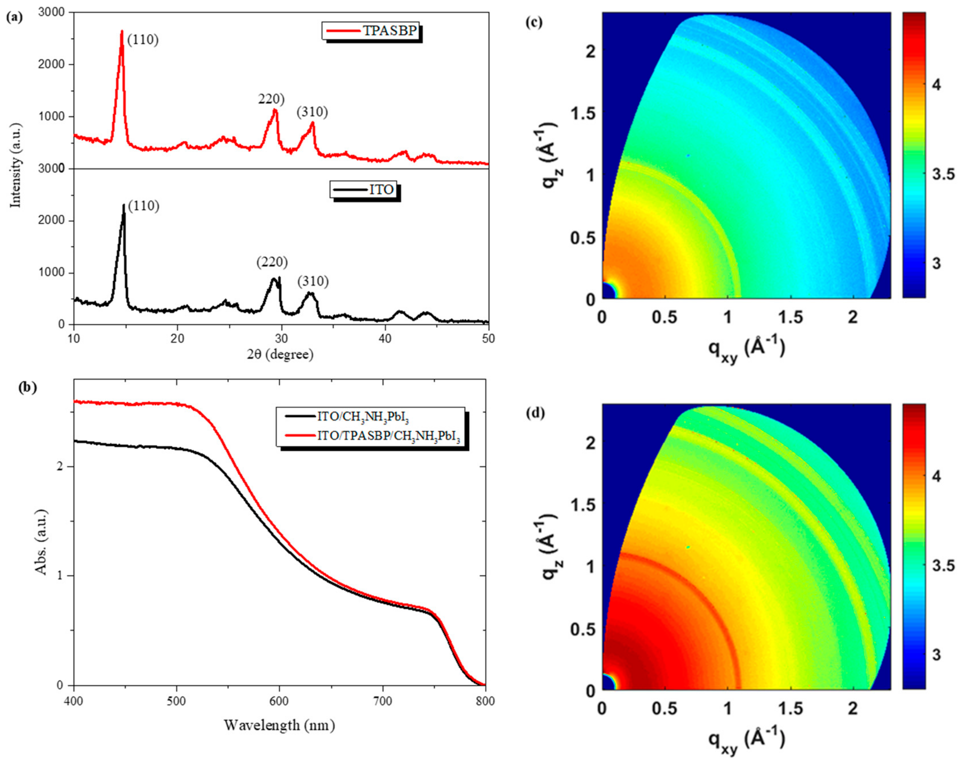
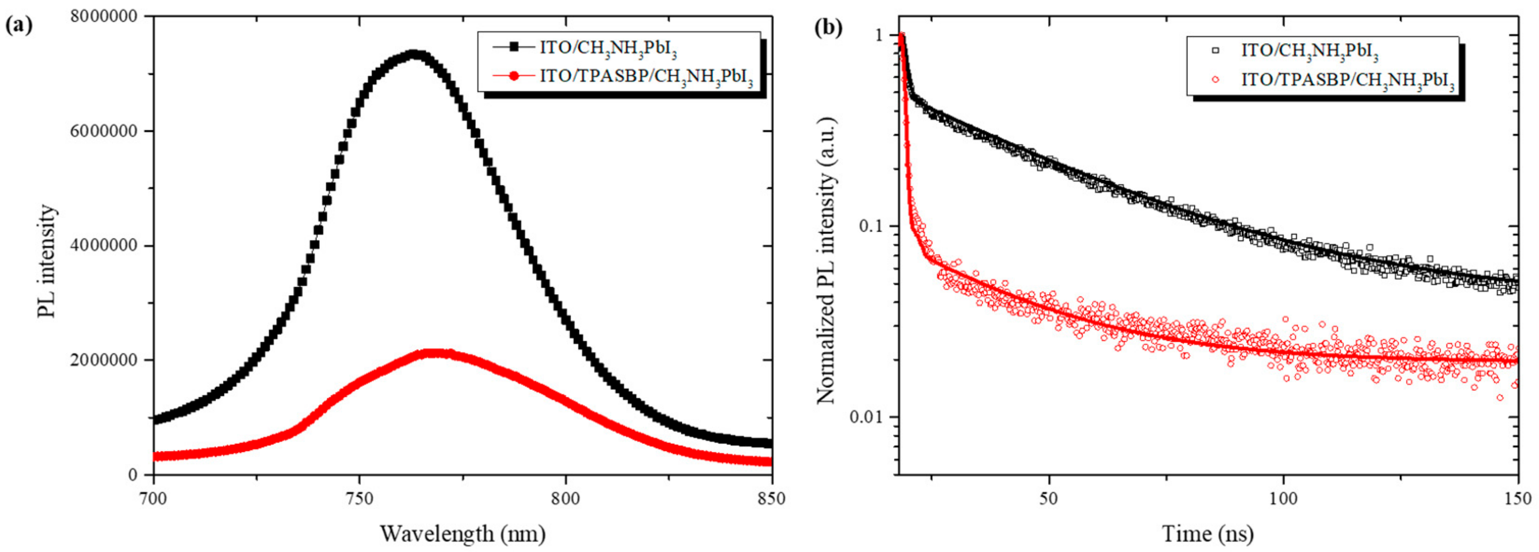
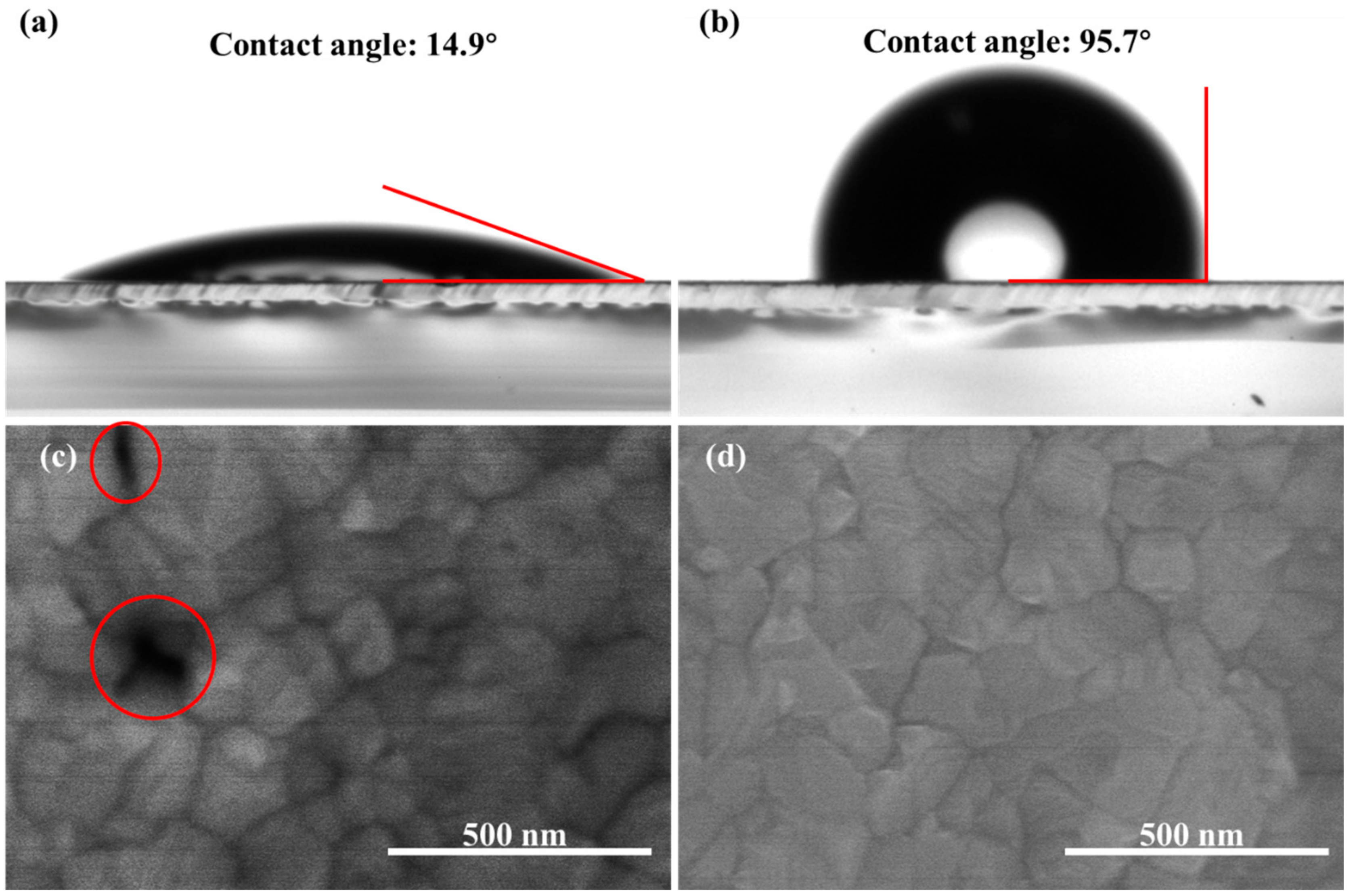
3.1. Characterization of the As-Prepared Perovskite Films

The hydrophobic property of the substrates is crucial for the nucleation of the perovskite [8,20]. Hence, the water contact angle images on the ITO and TPASBP surfaces were characterized, as shown in Figure 1a,b. The contact angles of water on the two different surfaces were 14.9° and 95.7° for the ITO and TPASBP, respectively. The larger contact angle means that the TPASBP is much more hydrophobic than a bare ITO surface. Because of the hydrophobic property of TPASBP, it hardly dissolves in many polar solvents like GBL, DMSO, N,N-dimethylformamide (DMF), etc. (as shown in Figure S1c). Hence, the hole-transporting layer and the CH3NH3PbI3 layer can be fabricated consecutively on ITO by a solution process. Moreover, the top-view SEM images of the CH3NH3PbI3 films on bare ITO and TPASBP (shown in Figure 1c,d) revealed a clear correlation between the hydrophobic property of the substrate surface and the CH3NH3PbI3 film morphology. It is obvious that there are clearly discerned pinholes in the perovskite film on bare ITO, whereas dense perovskite film without pinholes was obtained on TPASBP. Meanwhile, the average size of the CH3NH3PbI3 grains on TPASBP was ∼203 nm, which was larger than that on ITO (average grain size ∼160 nm). Figure S2 shows the corresponding grain size distribution of Figure 1c,b. The morphologies of CH3NH3PbI3 films on different substrates were further investigated by using AFM (as shown in Figure S3), where the CH3NH3PbI3 film based on hydrophobic TPASBP showed a smoother surface (root mean square (RMS) = 11.02 nm) relative to that on ITO (RMS = 14.69 nm). As shown in Figure S4, compared to hydrophilic ITO, the hydrophobic surface of TPASBP induced a lower density of perovskite nuclei after spin-coating the perovskite precursor, thus promoting the perovskite to grow into compact films with large grains after thermal annealing. Meanwhile, due to the reduction of perovskite nuclei on the substrate, the heterogeneous nucleation of perovskite was suppressed, and a much smoother perovskite film was realized.
To gain further insight into the effect of hydrophobic TPASBP surfaces on CH3NH3PbI3 crystallization, the XRD patterns of CH3NH3PbI3 films on ITO and TPASBP are shown in Figure 2a. No significant change in the diffraction peak ratio was observed, indicating the same crystal orientation of CH3NH3PbI3 film on both ITO and TPASBP. However, the X-ray diffraction peaks of CH3NH3PbI3 (110), (220), and (310), were more intense and sharper for perovskite film on hydrophobic TPASBP. In addition, two-dimensional GIWAXS patterns of perovskite films on ITO and TPASBP were measured and are shown in Figure 2c,d respectively. For the perovskite film deposited on TPASBP, the feature of CH3NH3PbI3 crystalline domains was clearer and the two-dimensional GIWAXS pattern exhibited stronger intensity at the diffraction peaks, indicating that the perovskite film on TPASBP showed finer ordering structures and better crystallization than that on ITO. The results from XRD and GIWAXS imply that the crystallization of CH3NH3PbI3 grown on the hydrophobic TPASBP was greatly improved in comparison with that on bare ITO. Hence, on the basis of improved CH3NH3PbI3 morphology and crystallization, the light absorption of perovskite film on TPASBP is enhanced in the whole wavelength range from 400 to 800 nm, especially from 400 to 550 nm, as presented by the UV–vis absorption spectra of perovskite films on ITO and TPASBP in Figure 2b.
Large grain size and compact CH3NH3PbI3 film tends to yield less trap states, which are beneficial for high-performance PSCs [8,29]. Hence, hole trap density in the CH3NH3PbI3 films was quantified by the dark I-V analysis for hole-only devices. Figure 3a,b show the I-V curves of the hole-only devices based on ITO and ITO/TPASBP substrates in the dark. It is clear that the linear regime (blue line) at low voltage indicates an ohmic response of the hole-only devices. With the increase of voltage, the current exhibits a rapid nonlinear rise (green line), presenting the transition to the trap-filled limit (TFL) regime in which all the available trap states are filled by the injected carriers. The TFL voltage VTFL is determined by the trap density [30,31]:
V TFL = en trap L 2 2 ε ε 0
where e is the elementary charge of the electron, L is the thickness of the CH3NH3PbI3 film, ε is the relative dielectric constant of CH3NH3PbI3 (ε = 30) [32], ε0 is the vacuum permittivity, and ntrap is the trap density. The onset voltage VTFL is linearly proportional to the density of trap states, ntrap; hence, the trap density can be calculated using Equation (1). Based on Figure 3a,b the VTFL values for the CH3NH3PbI3 films grown on ITO and TPASBP are 1.12 and 0.46 V, respectively. Correspondingly, the CH3NH3PbI3 film on bare ITO yields a hole trap density of 1.48 × 1016 cm−3, whereas the CH3NH3PbI3 film deposited on TPASBP has a hole trap density as low as 6.10 × 1015 cm−3.
On the basis of the above results, it was clear that a hydrophobic surface provided by TPASBP was beneficial for the formation of dense pinhole-free CH3NH3PbI3 film with a larger grain size relative to hydrophilic substrates, thus resulting in better crystallization of CH3NH3PbI3. Meanwhile, due to the improvement of CH3NH3PbI3 morphology and crystallization, the trap density was reduced significantly for the perovskite film fabricated on TPASBP compared with that on ITO, which induced less recombination loss in the PSCs.
Besides the hydrophobicity, TPASBP also has high hole mobility because of its linear π-conjugated structure, which has been illustrated before elsewhere [26,33]. Meanwhile, the results of steady-state PL and time-resolved PL (TRPL) shown in Figure 4 also revealed that the hole-extraction efficiency at the ITO/CH3NH3PbI3 interface was improved by using TPASBP. As presented in Figure 4a, a much stronger quenching effect on the PL of the CH3NH3PbI3 film on TPASBP was observed in comparison with that on ITO, suggesting an enhanced hole-extraction ability of TPASBP as an HTM. In order to further evaluate the hole-extraction rate, TRPL was performed and the decay curves are shown in Figure 4b. By a biexponential fitting of the dynamic TRPL data, the CH3NH3PbI3 film on ITO exhibited a longer lifetime of 32.26 ns, whereas the lifetime of CH3NH3PbI3 film grown on TPASBP was 21.87 ns. More details about carrier lifetime can be found in Table S1. The smaller PL lifetime of CN3NH3PbI3 fabricated on TPASBP indicates the reduced carrier recombination due to the more efficient hole extraction and transport in CH3NH3PbI3 film. The high mobility and the enhanced hole-extraction ability of TPASBP contributes to the high carrier collection efficiency of PSCs, thus leading to an enhancement of short-circuit current (Jsc).

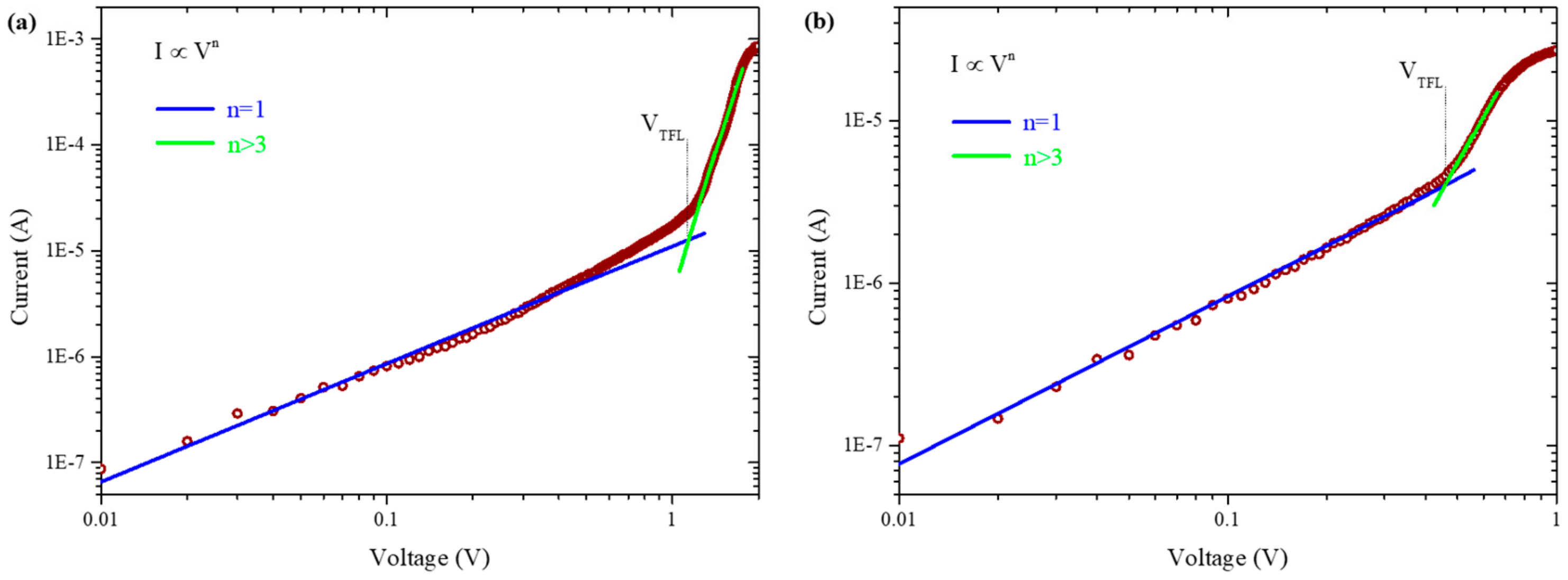
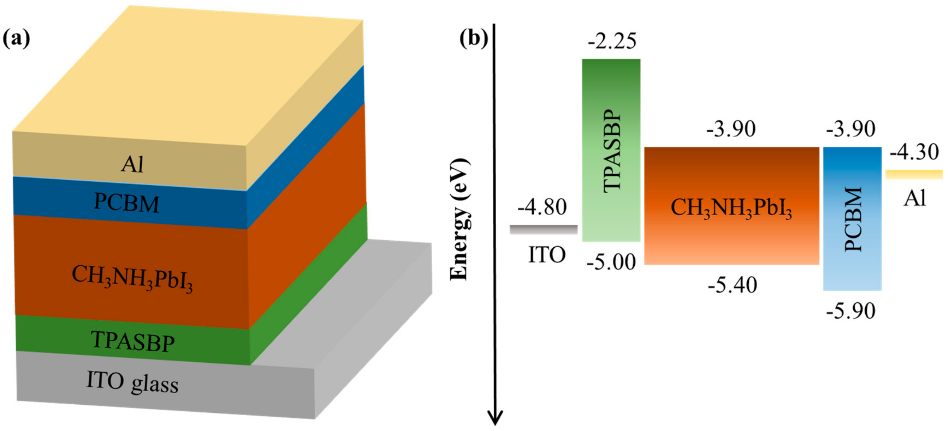
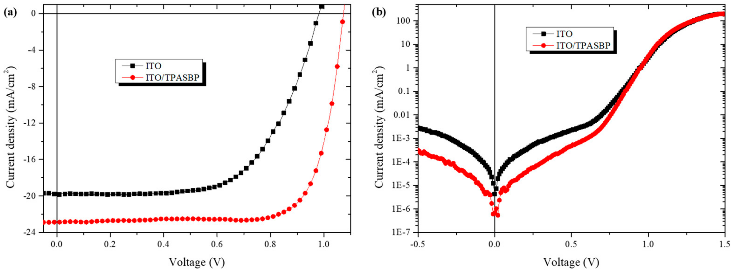
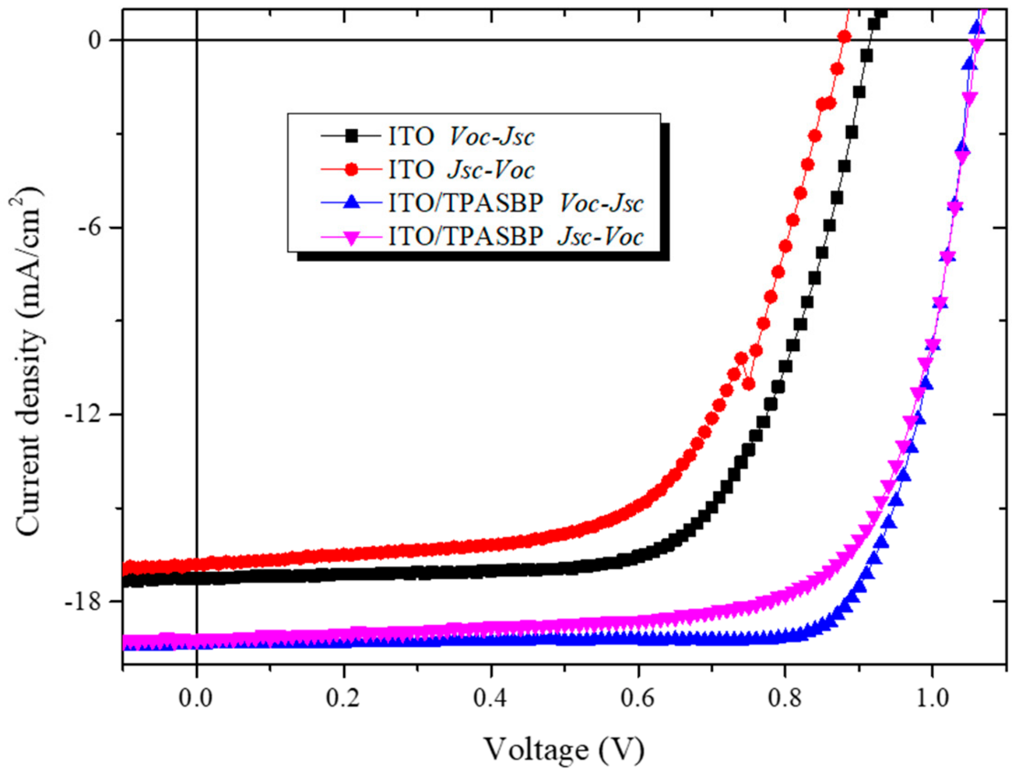
3.2. Photovoltaic Performance of PSCs

The influence of TPASBP on device performance was evaluated in inverted PSCs with a structure shown in Figure 5a, in which all layers between the electrodes were fabricated by spin-coating. The relative energy levels are presented in Figure 5b, where it can be seen that the highest occupied molecular orbital (HOMO) of TPASBP is between the work function of ITO and the valence band (VB) of CH3NH3PbI3, implying that the potential energy loss at the interface of TPASBP/CH3NH3PbI3 can be lowered.
The J-V characteristics of the inverted PSCs fabricated on TPASBP under 100 mW/cm−2 illumination (AM 1.5 G) are shown in Figure 6a. The same irradiation was carried out on PSCs based on bare ITO for comparison. PSCs fabricated on TPASBP afforded the best PCE of 18.72% with a Jsc of 22.87 mA/cm−2, an open circuit voltage (Voc) of 1.07 V, and a fill factor (FF) of 76.47% (listed in Table 1). The histogram of PCE shown in Figure S5 also indicates that inverted PSCs based on TPASBP exhibit good reproducibility, with an average efficiency of 17.23%. Meanwhile, the dependence of PSCs performance on the thickness of TPASBP is plotted in Figure S6, which reveals a thickness of 20 nm is optimal for TPASBP.
Dark J-V characteristics shown in Figure 6b indicates that the leakage current density at the low voltage scale was weakened dramatically in the PSCs with perovskite film grown on TPASBP. It has been reported that the leakage current is determined by RSh and consequent charge carrier recombination [34]. A reduction of leakage current means an increase of RSh and a reduction of charge carrier recombination in the device. The result of dark J-V was in good agreement with that of the reverse saturation current, which is discussed in the following part, revealing the remarkable role of TPASBP in preventing recombination in PSCs.
The improved FF and Voc strongly imply a reduction in recombination loss as a result of the utilization of TPASBP in inverted PSCs. The planar structured PSCs can be treated as single heterojunction diode. The electric parameters of the PSCs, including series resistance (Rs), and reverse saturation current density (J0), can be extracted from the J-V curves shown in Figure 6a according to the diode equation [35,36]:
J = J L J 0 exp e V + J × R S AK B T 1 V + J × R S R sh
where A is the ideality factor of the heterojunction, and KB and T are the Boltzmann constant and absolute temperature, respectively. Equation (2) can also be written as (where RSh is large enough):
dV dJ = AK B T e J SC J 1 + R S
ln J SC J = e AK B T V + J × R S + lnJ 0 .
The calculated values of A, Rs, J0 are listed in Table 2. For a well-behaved heterojunction solar cell, the ideality factor is typically in the range of 1.3 ˂ A ˂ 2 [36]. In the PSCs with perovskite film grown on TPASBP, the ideality factors obtained from Equations (3) and (4) are 1.56 and 1.72, respectively, which indicate that the PSCs based on TPASBP work well on the basis of a heterojunction model. It is also clear that Rs is much lower in the PSCs fabricated on TPASBP (1.19 Ω cm2) than the PSCs fabricated on ITO (5.68 Ω cm2). As also shown in Table 2, J0 for the PSCs with perovskite film grown on TPASBP is ∼2 orders of magnitude lower than those PSCs on ITO. J0 correlates with the carrier recombination in heterojunction solar cells, where a lower J0 corresponds to lower carrier recombination in PSCs. Therefore, the recombination in inverted PSCs is greatly lowered by using TPASBP. Meanwhile, according to the equation Voc = (AKBT/e)ln(Jsc/J0+1), smaller J0 also leads to larger Voc; hence, Voc in the PSCs with perovskite film deposited on TPASBP is higher than that on ITO.
Finally, the hysteresis of these devices was investigated, as displayed in Figure 7. According to the device performance of PSCs with respect to the scan direction under a 10 mv per point (voltage scan step) condition, it was clear that the PSCs based on ITO had much more serious J-V hysteresis while the PSCs fabricated on TPASBP gave almost the same values of Voc and Jsc with a small difference of FF under different scan modes. The restrain of hysteresis by TPASBP can be attributed to the improved quality of the CH3NH3PbI3 film and the significant decrease of recombination in the devices, which derived from the pinhole-free morphology and lower trap density of CH3NH3PbI3 grown on hydrophobic TPASBP, as described above.

4. Conclusions

In conclusion, the functions of a hydrophobic small molecular hole-transporting material in perovskite growth and device performance were explored in inverted PSCs. The hydrophobic TPASBP promoted the growth of CH3NH3PbI3 film deposited on it with pinhole-free coverage and a large grain size, leading to a decreased trap density and thus a remarkable reduction of recombination loss. TPASBP as an HTM also enabled effective hole extraction. Correspondingly, the PSCs with hydrophobic small molecular material as an HTM achieved a PCE as high as 18.72%. This work highlights the benefits of a hydrophobic surface for the crystalline growth of perovskite film, which provides an efficient way to obtain high-quality perovskite film for high performance inverted PSCs.

Supplementary Materials

The following are available online at https://www.mdpi.com/1420-3049/24/10/2027/s1, Figure S1: (a) Chemical structure of TPASBP, (b) transmittance spectra of TPASBP/ITO grass with ITO/grass as reference and UV-vis absorption spectra of TPASBP on ITO, (c) TPASBP solutions in DMF, GBL, and DMSO, respectively, with a concentration of 5 mg/mL, Figure S2: (a) Grain size distribution of the perovskite film in Figure 1(c), (b) grain size distribution of the perovskite film in Figure 1(d), Figure S3: 3D-AFM topography images of the perovskite films deposited on (a) bare and (b) TPASBP-covered ITO substrates, Figure S4: Depiction of the growth process for perovskite films on (a) hydrophilic ITO and (b) hydrophobic TPASBP, Figure S5: Distributions of (a) Jsc, (b) Voc, (c) FF, and (d) PCE obtained from eight identical cells for PSCs based on ITO and 13 identical cells for PSCs based on TPASBP, Figure S6: Dependence of the main parameters of the device performance on the thickness of TPASBP layer, Table S1: Time-resolved PL measurements, Table S2: The photovoltaic parameters of PSCs with different thicknesses of TPASBP.

Author Contributions

Conceptualization, Y.L. and Z.X.; Formal Analysis, Z.X., S.Z., D.S. and B.Q.; Investigation, Y.L., Y.Z. and J.M.; Data Curation, Y.L., Y.Z. and J.M.; Writing—Original Draft Preparation, Y.L. and Z.X.; Writing—Review and Editing, Z.X., S.Z., D.S. and B.Q.; Supervision, Z.X.; Funding Acquisition, Z.X. and S.Z.

Funding

This research was funded by the National Natural Science Foundation of China under Grant No.61575019, No.11474018, No.61775013, the National Key Research and Development Program of China under Grant No.2016YFB0401302, the Fundamental Research Funds for the Central Universities under Grant No.2016JBM066.

Acknowledgments

The authors also express the thanks to Xianggao Li for providing the material of TPASBP used in this work and appreciate the assistance of scientists of Diffuse X-ray Scattering Station for the measurement of XRD and GIWAXS at 1W1A, BSRF.

Conflicts of Interest

The authors declare no conflict of interest.

References

  1. Kojima, A.; Teshima, K.; Shirai, Y.; Miyasaka, T. Organometal Halide Perovskites as Visible-Light Sensitizers for Photovoltaic Cells. J. Am. Chem. Soc. 2009, 131, 6050–6051. [Google Scholar] [CrossRef]
  2. Burschka, J.; Pellet, N.; Moon, S.-J.; Humphry-Baker, R.; Gao, P.; Nazeeruddin, M.K.; Grätzel, M. Sequential Deposition as a Route to High-Performance Perovskite-Sensitized Solar Cells. Nature 2013, 499, 316–319. [Google Scholar] [CrossRef]
  3. Zheng, X.; Chen, B.; Dai, J.; Fang, Y.; Bai, Y.; Lin, Y.; Wei, H.; Zeng, X.C.; Huang, J. Defect Passivation in Hybrid Perovskite Solar Cells Using Quaternary Ammonium Halide Anions and Cations. Nat. Energy 2017. [Google Scholar] [CrossRef]
  4. Jiang, Q.; Zhao, Y.; Zhang, X.; Yang, X.; Chen, Y.; Chu, Z.; Ye, Q.; Li, X.; Yin, Z.; You, J. Surface Passivation of Perovskite Film for Efficient Solar Cells. Nat. Photonics 2019. [Google Scholar] [CrossRef]
  5. NREL Best Research-Cell Efficiencies. Available online: https://www.nrel.gov/pv/assets/pdfs/best-reserch-cell-efficiencies.20190411.pdf (accessed on 17 April 2019).
  6. Paek, S.; Zimmermann, I.; Gao, P.; Gratia, P.; Rakstys, K.; Grancini, G.; Nazeeruddin, M.K.; Rub, M.A.; Kosa, S.A.; Alamry, K.A.; et al. Donor-π-Donor Type Hole Transporting Materials: Marked π-Bridge Effects on Optoelectronic Properties, Solid-State Structure, and Perovskite Solar Cell Efficiency. Chem. Sci. 2016, 7, 6068–6075. [Google Scholar] [CrossRef] [PubMed]
  7. Zhang, J.; Hua, Y.; Xu, B.; Yang, L.; Liu, P.; Johansson, M.B.; Vlachopoulos, N.; Kloo, L.; Boschloo, G.; Johansson, E.M.J.; et al. The Role of 3D Molecular Structural Control in New Hole Transport Materials Outperforming Spiro-OMeTAD in Perovskite Solar Cells. Adv. Energy Mater. 2016. [Google Scholar] [CrossRef]
  8. Bi, C.; Wang, Q.; Shao, Y.; Yuan, Y.; Xiao, Z.; Huang, J. Non-Wetting Surface-Driven High-Aspect-Ratio Crystalline Grain Growth for Efficient Hybrid Perovskite Solar Cells. Nat. Commun. 2015. [Google Scholar] [CrossRef] [PubMed]
  9. Jhuo, H.-J.; Yeh, P.-N.; Liao, S.-H.; Li, Y.-L.; Sharma, S.; Chen, S.-A. Inverted Perovskite Solar Cells with Inserted Cross-Linked Electron-Blocking Interlayers for Performance Enhancement. J. Mater. Chem. A 2015, 3, 9291–9297. [Google Scholar] [CrossRef]
  10. Yan, W.; Li, Y.; Li, Y.; Ye, S.; Liu, Z.; Wang, S.; Bian, Z.; Huang, C. High-Performance Hybrid Perovskite Solar Cells with Open Circuit Voltage Dependence on Hole-Transporting Materials. Adv. Energy Mater. 2015, 16, 428–437. [Google Scholar] [CrossRef]
  11. Meng, L.; You, J.; Guo, T.-F.; Yang, Y. Recent Advances in the Inverted Planar Structure of Perovskite Solar Cells. Acc. Chem. Res. 2015, 49, 155–165. [Google Scholar] [CrossRef] [PubMed]
  12. Yan, W.; Ye, S.; Li, Y.; Sun, W.; Rao, H.; Liu, Z.; Bian, Z.; Huang, C. Hole-Transporting Materials in Inverted Planar Perovskite Solar Cells. Adv. Energy Mater. 2016. [Google Scholar] [CrossRef]
  13. Jeng, J.Y.; Chiang, Y.F.; Lee, M.H.; Peng, S.R.; Guo, T.F.; Chen, P.; Wen, T.C. CH3NH3PbI3 Perovskite/Fullerene Planar-Heterojunction Hybrid Solar Cells. Adv. Mater. 2013, 25, 3727–3732. [Google Scholar] [CrossRef] [PubMed]
  14. Heo, J.H.; Han, H.J.; Kim, D.; Ahn, T.K.; Im, S.H. Hysteresis-Less Inverted CH3NH3PbI3 Planar Perovskite Hybrid Solar Cells with 18.1% Power Conversion Efficiency. Energy Environ. Sci. 2015, 8, 1602–1608. [Google Scholar] [CrossRef]
  15. Wang, J.T.-W.; Wang, Z.; Pathak, S.; Zhang, W.; Wisnivesky-Rocca-Rivarola, F.; Huang, J.; Nayak, P.K.; Patel, J.B.; Yusof, H.A.M.; Vaynzof, Y. Efficient Perovskite Solar Cells by Metal Ion Doping. Energy Environ. Sci. 2016, 9, 2892–2901. [Google Scholar] [CrossRef]
  16. Luo, D.; Yang, W.; Wang, Z.; Sadhanala, A.; Hu, Q.; Su, R.; Shivanna, R.; Trindade, G.F.; Watts, J.F.; Xu, Z.; et al. Enhanced Photovoltage for Inverted Planar Heterojunction Perovskite Solar Cells. Science 2018, 360, 1442–1446. [Google Scholar] [CrossRef] [PubMed]
  17. Chen, W.; Wu, Y.; Yue, Y.; Liu, J.; Zhang, W.; Yang, X.; Chen, H.; Bi, E.; Ashraful, I.; Grätzel, M. Efficient and Stable Large-Area Perovskite Solar Cells with Inorganic Charge Extraction Layers. Science 2015, 350, 944–948. [Google Scholar] [CrossRef] [PubMed]
  18. Rao, H.; Ye, S.; Sun, W.; Yan, W.; Li, Y.; Peng, H.; Liu, Z.; Bian, Z.; Li, Y.; Huang, C. A 19.0% Efficiency Achieved in CuOx-Based Inverted CH3NH3PbI3−xClx Solar Cells by an Effective Cl Doping Method. Nano Energy 2016, 27, 51–57. [Google Scholar] [CrossRef]
  19. Xu, B.; Bi, D.; Hua, Y.; Liu, P.; Cheng, M.; Grätzel, M.; Kloo, L.; Hagfeldt, A.; Sun, L. A Low-Cost Spiro [fluorene-9, 9′-xanthene]-Based Hole Transport Material for Highly Efficient Solid-State Dye-Sensitized Solar Cells and Perovskite Solar Cells. Energy Environ. Sci. 2016, 9, 873–877. [Google Scholar] [CrossRef]
  20. Huang, C.; Fu, W.; Li, C.-Z.; Zhang, Z.; Qiu, W.; Shi, M.; Heremans, P.; Jen, A.K.-Y.; Chen, H. Dopant-Free Hole-Transporting Material with a C3h Symmetrical Truxene Core for Highly Efficient Perovskite Solar Cells. J. Am. Chem. Soc. 2016, 138, 2528–2531. [Google Scholar] [CrossRef]
  21. Wang, Q.; Bi, C.; Huang, J. Doped Hole Transport Layer for Efficiency Enhancement in Planar Heterojunction Organolead Trihalide Perovskite Solar Cells. Nano Energy 2015, 15, 275–280. [Google Scholar] [CrossRef]
  22. Krishnamoorthy, T.; Kunwu, F.; Boix, P.P.; Li, H.; Koh, T.M.; Leong, W.L.; Powar, S.; Grimsdale, A.; Grätzel, M.; Mathews, N. A Swivel-Cruciform Thiophene Based Hole-Transporting Material for Efficient Perovskite Solar Cells. J. Mater. Chem. A 2014, 2, 6305–6309. [Google Scholar] [CrossRef]
  23. Xu, Q.; Lu, Z.; Zhu, L.; Kou, C.; Liu, Y.; Li, C.; Meng, Q.; Li, W.; Bo, Z. Elimination of the J-V Hysteresis of Planar Perovskite Solar Cells by Interfacial Modification with a Thermo-Cleavable Fullerene Derivative. J. Mater. Chem. A 2016, 4, 17649–17654. [Google Scholar] [CrossRef]
  24. Wang, Z.K.; Gong, X.; Li, M.; Hu, Y.; Wang, J.M.; Ma, H.; Liao, L.S. Induced Crystallization of Perovskites by a Perylene Underlayer for High-Performance Solar Cells. ACS Nano 2016, 10, 5479–5489. [Google Scholar] [CrossRef] [PubMed]
  25. Jiang, Q.; Chu, Z.; Wang, P.; Yang, X.; Liu, H.; Wang, Y.; Yin, Z.; Wu, J.; Zhang, X.; You, J. Planar-Structure Perovskite Solar Cells with Efficiency beyond 21%. Adv. Mater. 2017. [CrossRef] [PubMed]
  26. Wang, J.; Wang, S.; Li, X.; Zhu, L.; Meng, Q.; Xiao, Y.; Li, D. Novel Hole Transporting Materials with a Linear π-Conjugated Structure for Highly Efficient Perovskite Solar Cells. Chem. Commun. 2014, 50, 5829–5832. [Google Scholar] [CrossRef] [PubMed]
  27. Seo, J.; Park, S.; Kim, Y.C.; Jeon, N.J.; Noh, J.H.; Yoon, S.C.; Seok, S.I. Benefits of very Thin PCBM and LiF Layers for Solution-Processed p–i–n Perovskite Solar Cells. Energy Environ. Sci. 2014, 7, 2642–2646. [Google Scholar] [CrossRef]
  28. Jeon, N.J.; Noh, J.H.; Kim, Y.C.; Yang, W.S.; Ryu, S.; Seok, S.I. Solvent Engineering for High-Performance Inorganic–Organic Hybrid Perovskite Solar Cells. Nat. Mater. 2014, 13, 897–903. [Google Scholar] [CrossRef] [PubMed]
  29. Xiao, Z.; Dong, Q.; Bi, C.; Shao, Y.; Yuan, Y.; Huang, J. Solvent Annealing of Perovskite-Induced Crystal Growth for Photovoltaic-Device Efficiency Enhancement. Adv. Mater. 2014, 26, 6503–6509. [Google Scholar] [CrossRef] [PubMed]
  30. Shi, D.; Adinolfi, V.; Comin, R.; Yuan, M.; Alarousu, E.; Buin, A.; Chen, Y.; Hoogland, S.; Rothenberger, A.; Katsiev, K. Low Trap-State Density and Long Carrier Diffusion in Organolead Trihalide Perovskite Single Crystals. Science 2015, 347, 519–522. [Google Scholar] [CrossRef] [PubMed]
  31. Yang, D.; Yang, R.; Ren, X.; Zhu, X.; Yang, Z.; Li, C.; Liu, S. Hysteresis-Suppressed High-Efficiency Flexible Perovskite Solar Cells Using Solid-State Ionic-Liquids for Effective Electron Transport. Adv. Mater. 2016, 28, 5206–5213. [Google Scholar] [CrossRef] [PubMed]
  32. Laban, W.A.; Etgar, L. Depleted Hole Conductor-Free Lead Halide Iodide Heterojunction Solar Cells. Energy Environ. Sci. 2013, 6, 3249–3253. [Google Scholar] [CrossRef]
  33. Li, Y.; Xu, Z.; Zhao, S.; Qiao, B.; Huang, D.; Zhao, L.; Zhao, J.; Wang, P.; Zhu, Y.; Li, X.; et al. Highly Efficient p-i-n Perovskite Solar Cells Utilizing Novel Low-Temperature Solution-Processed Hole Transport Materials with Linear π-Conjugated Structure. Small 2016, 12, 4902–4908. [Google Scholar] [CrossRef] [PubMed]
  34. Wetzelaer, G.J.A.; Scheepers, M.; Sempere, A.M.; Momblona, C.; Ávila, J.; Bolink, H.J. Trap-Assisted Non-Radiative Recombination in Organic–Inorganic Perovskite Solar Cells. Adv. Mater. 2015, 27, 1837–1841. [Google Scholar] [CrossRef] [PubMed]
  35. Song, D.; Ji, J.; Li, Y.; Li, G.; Li, M.; Wang, T.; Wei, D.; Cui, P.; He, Y.; Mbengue, J.M. Degradation of Organometallic Perovskite Solar cells Induced by Trap States. Appl. Phys. Lett. 2016. [CrossRef]
  36. Shi, J.; Dong, J.; Lv, S.; Xu, Y.; Zhu, L.; Xiao, J.; Xu, X.; Wu, H.; Li, D.; Luo, Y. Hole-Conductor-Free Perovskite Organic Lead Iodide Heterojunction Thin-Film Solar Cells: High Efficiency and Junction Property. Appl. Phys. Lett. 2014. [CrossRef]
Figure 1. Contact angles of (a) indium tin oxide (ITO) and (b) ITO/4,4′-Bis(4-(di-p-toyl)aminostyryl)biphenyl (TPASBP) surfaces, and corresponding top-view SEM images of the perovskite films grown on (c) bare and (d) TPASBP-covered ITO substrates; the red circles in Figure 1c indicate pinholes in perovskite film.
Molecules 24 02027 g001
Figure 2. (a) X-ray diffraction (XRD) patterns, and (b) UV–vis absorption spectra of CH3NH3PbI3 films on ITO and TPASBP substrates, (c) and (d) two-dimensional grazing-incident wide-angle X-ray scattering (GIWAXS) patterns of CH3NH3PbI3 films on ITO and TPASBP, respectively.
Molecules 24 02027 g002
Figure 3. Characteristic current-voltage (I-V) trace (red markers) showing two different regimes for (a) ITO/CH3NH3PbI3/Au, and (b) ITO/TPASBP/CH3NH3PbI3/Au. A linear ohmic regime (I ∞ V, blue line) is followed by the trap-filled regime, marked by a steep increase in current (I ∞ Vn > 3, green line).
Molecules 24 02027 g003
Figure 4. (a) Steady-state PL spectra, and (b) time-resolved PL (TRPL) decay curves of CH3NH3PbI3 films on ITO and ITO/TPASBP substrates.
Molecules 24 02027 g004
Figure 5. (a) Schematic device structure of the inverted PSCs constructed by ITO/TPASBP/CH3NH3PbI3/PCBM/Al, (b) schematic energy level diagram of each layer.
Molecules 24 02027 g005
Figure 6. (a) Current density-voltage (J-V) characteristics of the best PSCs based on bare ITO and TPASBP-covered ITO under irradiation of 100 mW/cm−2, (b) dark J-V characteristics of the PSCs with and without TPASBP.
Molecules 24 02027 g006
Figure 7. J-V characteristics of inverted PSCs with different scanning directions.
Molecules 24 02027 g007
Table 1. The photovoltaic parameters of PSCs with perovskite film fabricated on ITO and ITO/TPASBP, respectively.
PSCsVoc
[V]
Jsc
[mA/cm2]
FF
[%]
PCE
[%]
Average PCE a
[%]
ITO0.9819.7262.3512.0511.07± 0.97
ITO/TPASBP1.0722.8876.4718.7217.23 ± 0.79
a the average PCE of PSCs based on ITO was obtained from 8 identical cells and the average PCE of PSCs based on TPASBP was obtained from 13 identical cells.
Table 2. Fitted electrical parameters of PSCs with perovskite film fabricated on ITO and ITO/TPASBP, respectively.
PSCsA1 aA2 bRS (Ωcm2)J0 (mAcm−2)
ITO2.272.225.682.27 × 10-4
ITO/TPASBP1.561.721.192.38 × 10-6
a A1 and (series resistance) Rs were obtained from Equation (3), b A2 and (reverse saturation current density) J0 were obtained from Equation (4).

