Abstract
Nowadays, a huge amount of digital data is frequently changed among different embedded devices over wireless communication technologies. Data security is considered an important parameter for avoiding information loss and preventing cyber-crimes. This research article details the low power high-speed hardware architectures for the efficient field programmable gate array (FPGA) implementation of the advanced encryption standard (AES) algorithm to provide data security. This work does not depend on the Look-Up Table (LUTs) for the implementation the SubBytes and InvSubBytes stages of transformations of the AES encryption and decryption; this new architecture uses combinational logical circuits for implementing SubBytes and InvSubBytes transformation. Due to the elimination of LUTs, unwanted delays are eliminated in this architecture and a subpipelining structure is introduced for improving the speed of the AES algorithm. Here, modified positive polarity reed muller (MPPRM) architecture is inserted to reduce the total hardware requirements, and comparisons are made with different implementations. With MPPRM architecture introduced in SubBytes stages, an efficient mixcolumn and invmixcolumn architecture that is suited to subpipelined round units is added. The performances of the proposed AES-MPPRM architecture is analyzed in terms of number of slice registers, flip flops, number of slice LUTs, number of logical elements, slices, bonded IOB, operating frequency and delay. There are five different AES architectures including LAES, AES-CTR, AES-CFA, AES-BSRD, and AES-EMCBE. The LUT of the AES-MPPRM architecture designed in the Spartan 6 is reduced up to 15.45% when compared to the AES-BSRD.
1. Introduction
Information is treated as the most valuable asset in present day since about billions of items of information are processed and shared per second in this technological world. This large amount of information must be processed and shared in a very secure manner. Since information is treated as a most valuable thing, there is also a very high chance of piracy or alteration of this information by an unintended user [1,2,3,4,5]. Unauthorized change and availability of the original information also form the major goal of the researchers to keep the information secure. Researchers use cryptographic algorithms to keep information secret while transmitting and receiving information on an insecure channel. Cryptographic algorithms perform encryption operations on the original plain text before transmitting and perform decryption operation after receiving the encrypted text from the insecure channel. A secret key is used for both encryption and decryption operations. Based on the usage of a number of secret keys, cryptographic algorithms can be classified as symmetric and asymmetric algorithms. Furthermore, algorithms can be classified as block and stream cipher algorithms based on the number of bits, and the algorithms can operate simultaneously [6,7,8,9,10]. Generally, these cryptographic algorithms are utilized in different applications such as banking applications, military and government [11], and critical infrastructures such as Smart Grid [12,13].
In 2001, the National Institute of Standards and Technology (NIST) published a symmetric algorithm called AES which is a replacement of the data encryption standard (DES) [14,15]. AES is one of the extensively used symmetric key cryptography algorithm that uses same key for both the encryption and decryption of the sensitive data [16,17]. In the last two decades, researchers have developed many cryptographic efficient algorithms. Still, AES stands as the most secure cryptographic algorithm due to its cost effectiveness and easier implementation in both hardware and software. AES is a non-Feistel cipher that has the same rounds of operations in both the encryption and decryption processes. It is being proved that hardware implementations of the AES is more secure and faster than that of software implementations [18,19,20,21]. The AES is categorized as AES-128, AES-192 and AES-256 based on the length of the key. Here, the 128, 192, and 256 indicates the length of the key used during the cryptographic process [22]. A high-performance modern microprocessors are used to design the AES for satisfying the high throughput requirements in the desired applications. However, a VLSI based hardware description language (HDL) design of AES is accomplished to obtain the low silicon area and high speed [23]. An architectural modification such as pipelining, subpipelining, and loop-unrolling are used to enhance the throughput and operational frequency [24,25]. A high-speed AES design is obtained by using the hardware architectures with unwound loops and pipelines. However, this architecture faces the high area consumption while accomplishing the encryption operation [26].
The traditional symmetric/asymmetric algorithms are used for the data security such as DES [27,28,29], triple DES [30], elliptic curve cryptography (ECC) [31,32,33,34], Rivest–Shamir–Adleman (RSA) [35], etc. In these algorithms, ECC and RSA are well known asymmetric-key-cryptography that use public keys for encryption/decryption processes. In the conventional general-purpose processors, the conventional cryptographic algorithms obtain less speed and demands higher resources during the computation process [36]. For example, the RSA has a complex design and low-level efficiency, and hence it is not appropriate for low-area applications [37]. Nowadays, some of the block ciphers from the symmetric algorithms are also used for the data security purpose and examples of the block cipher are SIMON [38], SEED [39], KLEIN [40], HIGHT [41], KASUMI [42], CLEFIA [43], PRESENT [44,45], etc. These low complexity light weight block ciphers can be used in wireless communications (i.e., internet of things (IoT) applications). If the number of devices in the certain communication increases, then it creates difficult issues such as higher hardware utilization and delay. Therefore, theses block ciphers aren’t suitable for the low area applications [46].
Kumar, K et al. [47] presented the design of lightweight AES (LAES) algorithm in Artix-7 and Kintex-7 FPGAs to secure the voice data. The operation of the mix column was decreased in the LAES algorithm than the conventional AES algorithm. After decreasing the operations of the mix column, the 128-bit cipher text was acquired from the results of shift rows operation. The reduction in the mix column process was resulted in the less delay as well as it was used to minimize the logic operation. Therefore, the complexity of this LAES algorithm was decreased while encrypting the voice data. However, the reduction in the mix column was increased the utilization of the multiplexers. Shahbazi, K. and Ko, S.B [48] developed the high throughput FPGA design of AES algorithm in counter (CTR) mode on Xilinx Virtex-5 for high traffic applications. In this work, the AES was modified based on the following two strategies: (1) sub-bytes and shift-rows were exchanged for the first nine rounds, and (2) the shift rows were combined with added round keys. Here, the inner pipelining, outer pipelining, and loop-unrolling were used for obtaining a higher throughput. A new-affine-transformation, which was a combination of inverse isomorphic and affine transformation, was used to minimize the area of the Sub-Bytes. Moreover, the operation of the mix-column was separated into two stages for obtaining an equal latency among the stages. However, the execution of the mix column operation in on clock cycle was resulted in higher latency.
Arul Murugan, C et al. [49] presented iterative architecture of AES-128 encryption for enhancing the security. The LUT was used in the composite field arithmetic (CFA) to perform the multiplication in the S-box. Subsequently, the area was minimized by using the updated architecture of the S-box in the AES. Additionally, the Vedic multiplier was used in the operation of mix columns for minimizing the hardware resources of the AES. Here, three different FPGA devices such as Virtex-4, Virtex-5, and Spartan 3 devices were used to design the AES algorithm. The utilization of the CFA resulted in higher speeds in the process of sub-byte transformation. However, the architecture of the mix column transformation was highly complex when compared to the architecture of the shift-row transformation. Wegener, F et al. [50] developed the extended version of the AES in Spartan 6 for compromising the requirements of area and latency. The Bit-Serial Rotational Design (BSRD) was used instead of the S-box in the AES architecture. Moreover, the nonlinear proportion was significantly decreased by using the rotational symmetry technique for implementing the S-box of the AES algorithm. The linear operation was replicated and executed independently in the AES algorithm, which increased its area.
Madhavapandian and Maruthu Pandi [51] presented the design of secure architecture for the Transmission Control Protocol/Internet Protocol (TCP/IP). The protection over the TCP/IP protocol was achieved by using the 128 bit of AES algorithm. Next, the AES architecture was optimized for reducing the power consumption and cost. Moreover, an improved compressed structure for the mix columns was used along with the efficient mix column Boolean expression (EMCBE) for optimizing the structure of the AES. Here, the AES algorithm was designed and implemented using the Virtex 6 algorithm. However, the technique of gate replacement used for minimizing the delay affected the scalability of this AES architecture. Zodpe and Sapkal [52] developed the pseudo-random noise (PN) sequence generator for generating the values of the S-box. The distinct sequence of random numbers was generated by using the PN generator based on the feedback taps and initial seed value. An efficiency of the cryptosystem was improved based on the features of the PN sequence generator. Here, the requirement for applying the external key was avoided by using an initial key generation technique. However, the utilization of hardware resources of the AES was high, when it was designed by using the non-pipelined stages.
Sikka et al. [53] presented the high throughput FPGA implementation for the AES algorithm. Here, the AES algorithm was designed for the automotive applications. Specifically, the Vivado high-level synthesis (HLS) tool was used to design the AES with a 128-bit of key size and block size of 10 rounds. This HLS was used mainly based on the application-specific bit widths that used to design the FPGA. The implementation of AES using the HLS was used to improve the speed. However, the delay of this AES algorithm was increased because of the frequent re-calculation of the signal width for each input, output and intermediate value.
The existing methods are analyzed and explained as follows: for a better implementation of the AES, the hardware resources (e.g., slices and LUT) are required less during the encryption/decryption process. But, the requirements of the multiplexers are increased, when mix column operation is minimized in the LAES [47]. The replication of linear operation increases the area of the AES in encryption/decryption processes [50]. Moreover, the hardware resources of the AES are improved when it is designed by using the non-pipelined stages [52]. The latency is increased in the AES operation in the mix column operation [48]. Next, the delay of the AES is increased due to the frequent re-calculation of the signal width [53]. In order to overcome the aforementioned issues, an MPPRM based SubBytes transformation is designed to reduce the hardware resources used during the encryption/decryption process. Additionally, the delay element added in the AND gate of the MPPRM is used to minimize the delay caused in the encryption process.
Generally, the SubBytes transformation processed in the AES is considered as bottleneck during the encryption process, since the transformation calculates the most resource demanding multiplicative inverse function at the finite field arithmetic operation. The SubBytes transformation designed by using the read only memory creates an inappropriate delay in the AES encryption/decryption [54]. From the modifications of pipelining, subpipelining, and loop-unrolling, the subpipelining is used to achieve maximum speed with minimal area occupancy. LUT based approaches used in the SubBytes and InvSubBytes transformation stages causes much delay than the total delay of all of the other transformations. Therefore, in this work LUT based transformation is replaced with the minimal delay combinational circuits. Composite field architecture is one such architecture that provides the required logics. Also, composite field arithmetic structure has been implemented with subpipelinining architecture in this work. However, delays can also be reduced by eliminating the delays occurring due to dynamic hazards that take place in combination circuits. This is achieved by implementing SubBytes and InvSubBytes transformation in MPPRM architecture. Here, both the architectures are explored and hardware utilization comparisons are made to explore the most suitable architecture. Algorithms used for secure communication must withstand the cryptanalytic attacks which aim to find the secret key based on the techniques and mathematical operations used in converting plain text to cipher text. With the aim of optimizing the AES structure, a MPPRM based SubBytes transformation is accomplished for achieving the less area and lesser hardware resources during the FPGA implementation.
The most important contributions of this research work are given as follows:
This work uses composite field arithmetic structure both SubBytes and InvSubBytes transformations with the speed efficient subpiplining structure. Earlier approach of implementing CFA is to decompose GF(28) as GF(((22)2)2). Where in this work GF(28) is decomposed as GF((24)2).
MPPRM architecture is used for both SubBytes and InvSubBytes transformations for minimizing the AND and XOR gates to minimize the hardware resources used in the encryption/decryption process.
In this work, key expansion architecture is used to provide 128-bit key for subpipelined structure. A speed efficient AES-MPPRM architecture is achieved, because of the delay element added in the AND gate output.
The organization of the paper is given as follows: The information about the conventional AES algorithm is provided in Section 2. Section 3 provides the detailed explanation about the AES-MPPRM architecture. The modified new architecture in key expansion module is detailed in Section 4. Section 5 gives the results and discussion of the AES-MPPRM architecture. The conclusion of this research paper is provided in Section 6.
2. Related Works
The information about the conventional AES encryption and decryption process is provided in this section. This section contains the process of substitution, shift rows, mix columns, added round keys, key expansion architecture, subpipelined architecture, and composite field arithmetic operation.
2.1. AES Algorithm
Advanced encryption standard (AES) is a symmetric cryptographic algorithm, in which a single secret key is used for both encryption and decryption operations. AES has three different versions and each version operates at different bit levels of secret key. Based on the number of bits in the secret key, AES can be classified as AES-128, AES-192, or AES-256. Number of rounds of encryption and decryption operation for each version also varies from one another and it is given in Table 1.

Table 1.
Different types of AES.
Every round in the AES algorithm uses different subkeys, which are generated from the main original key. Although key sizes are different for each version, no of bits from the original data to be communicated securely remains same for all the versions. Data block size is 128 bits for all of the three versions of the AES algorithm. Number of rounds denotes the number of encryption operation takes places for a single data block with different subkeys obtained from the key expansion process. Diffusion and confusion process for each round remains same. Initially, the main key is utilized for pre round transformation and other subkeys are used in each round. So number of keys required will be always higher than the amount of rounds in AES versions.
2.2. AES Encryption and Decryption
AES is generally a non-Fiestel block cipher cryptographic algorithm that encrypts plain original text into encrypted cipher text with the help of secret key. Secret key lengths differ for different versions of the AES algorithm, as mentioned in Table 1. The same algorithm which is utilized to transform the plain text into cipher text can also be used to get back the plain text from the cipher text by using a secret key used in the encryption process. Except for the last round in all of the AEs versions, all of the other rounds will have the following four operations in both the encryption and decryption processes. Before proceeding to the encryption process, 128-bit plain text is grouped into a state matrix of order 4 × 4 with each element in the matrix is represented as a word (2 bytes).
2.2.1. Substitution Transformation
Substitution is a process in which a byte value is replaced by another byte. Only non-linear process involved in the AES algorithm is substitution.
Each byte in the state matrix is considered as a polynomial in the Galois Field 28. Next, the affine transformation and matrix multiplication are used to transform the byte. Substitution can also be conducted directly using the RijndaelS-box. In decryption, inverse S-box is used for the substitution process. Substitution step introduces the actual confusion to the original data, forms the important step in preserving the original data from unauthorized access.
2.2.2. Shift Rows
The rows of state array are periodically shifted in the shift row phase. Here, the second, third, and fourth rows are shifted left by one, two and, three times, respectively, where the first row remains unaffected in the given input. Moreover, the rows are shifted right for accomplishing the decryption operation. Shift row is the first process of diffusion in the AES algorithm. This shift row process is invertible.
2.2.3. Mix Column Transformation
Similar to the operation of the shift row, the mix column operation is carried out in the column level. Here, the matrix multiplication is used to perform the operation of the mix column. The mix column and inv mix column operation are expressed in the following Equations (1) and (2).
where and are the output obtained after mix column operation; and are the input for mix column operation obtained as the output of Shift row operation.
2.2.4. Add Round Key
The important operation in the AES algorithm is add round key, since all of the earlier three steps are invertible. Without this operation, AES encryption becomes meaningless. Function of secret key takes place at the add round key operation. In this operation the original secret key or several subkeys are first arranges as a state matrix of 4 × 4 order. Matrix addition between keys and plain text is the operation in the add round key. As a result of this add round key operation, we get the cipher text.
All the above four operations are repeated for n number of times, where n denotes the number of rounds in the AES version. For every iteration, a different subkey is used. Therefore, for n number of rounds, n number of subkeys must be derived. Derivation of several subkeys from single main secret key is referred as key expansion process. Operation in the key expansion process or key schedule process must be carefully implemented, since the relation between subkeys should not be exploited easily. The mathematical way is followed by the key expansion process for deriving the different keys from the single way. In AES-MPPRM architecture, the time consumption is minimized for obtaining the subkeys from main key.
2.3. Key Expansion Architecture
AES-128 key expansion process is discussed in this section. In the key expansion process, the main secret key of 128 bit is divided into four words, each with 32-bit length. For AES-128, 10 subkeys must be derived from main original secret key. These subkeys are used in process of producing cipher text from plain text. Figure 1 clearly explains the process of key scheduling or key expansion. Mathematical operations are performed with the main key to derive the subkeys. Interdependency with the previous subkey makes the key expansion process efficient.
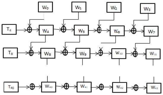
Figure 1.
Existing Key Expansion Architecture.
Mathematical operation takes place at the word level and consecutive four words are combined together to form a subkey. For example, W4, W5, W6, and W7 are combined to form first subkey. Key expansion algorithm generates a total of 4 (Nr + 1) words. Mathematical operation used here is just an EXOR operation between a previous word and a word from the previous subkey.
Generation of Temporary Word
Temporary word is the most important thing in key expansion process, since the only non-linear process involved in generation of subkeys is in the process of generation of temporary word. The first word of every subkey is generated as a result of EXOR operation between its corresponding temporary word and a word from a previous subkey. Three operations are performed in a word to create a temporary word. Substitution, Rotation and EXOR are the three operations which are performed in the process of creating a temporary word. For AES-128, temporary words are necessary to create W4, W8, W12, W16, W20, W24, W28, W32, W36, W40. Simply for i ≠ 4Nr, temporary words are not needed. Equation (3) represents the generation of the temporary word.
where, ‘i’ denotes the word number and ‘Nr’ denotes the round number in AES.
The rotword routine is identical to the Shift row routine, however it is used for the only one row. Moreover, the subword is similar to the Sub byte routine. The value of R constant differed for each round is provided in the Table 2.
Table 2.
R constant values for each rounds of AES.
2.4. Subpipelined Architecture
As stated in the first section subpipelining architectural optimization achieves maximum speed and great throughput than that of pipelining and folded architectures. To implement subpipelining, approach registers are inserted between each stage of every round and registers are also inserted between the rounds to store the intermediate results. One of the main advantages of subpipelining over folder structures is that it can simultaneously operate multiple blocks of data. Subpipelining involves splitting each round of AES operation into n substages, as shown in Figure 2. The total delay in each substages involves set up delay, propagation delay, multiplexer delay, and combinational circuits delay (which are very small). Here, each substages within a round are divided with equal delay, with extra registers included within and between the rounds adds up more area to the architecture. It is noted that when the number of substages with equal delay are increased for each round, improvement in speed can be achieved. But dividing the rounds into substages does not improve the speed of the architecture due to the delay caused by adding a greater number of registers. Some of the component of rounds may give minimal delay when compared to the delay provided by the substages of that component. This is entirely because of the accumulated delay due to the additional registers. In those cases it is better not to divide those components into substages. Although subpipelining makes the blocks to be processed simultaneously, the average number of clock cycles for processing a block remains same. This is also the reason for not dividing each round after particular parts. As we know that that individual logic gates delay is the highest undividable delay of any combinational logics in non LUT based design. Based on this result, rounds can be divided into substages.
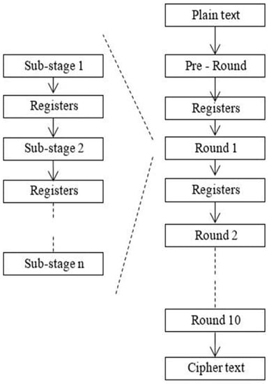
Figure 2.
Illustration of the subpipelining architecture.
2.5. Composite Field Arithmetic
As stated in the previous section, composite field arithmetic is implemented to increase speed as well as throughput of the AES encyptor and AES decryptor. For SubByte transformation, a byte must undergo a multiplicative inversion process and affine transformation. Composite field arithmetic is used to find the multiplicative inverse of a byte without much complexity overload. CF is denoted as GF ((2n)m) and Gf (2k) is isomorphic to GF ((2n)m) when K = nm. It is employed by mapping lower order GF to higher order GF.
The GF (28) is built from mapping GF by using the Equation (4).
The values of ɸ and ʎ are chosen as 10 and 1100, respectively, to make the above three equations as an irreducible equation. Isomorphic mapping function f(x) = δ × x and its inverse f(x)−1 are to be mapped to its composite field element and its inverse field element, where δ is a matrix with binary digits as its elements based on the GF (28) elements and its composite field elements. Suitable matrix for composite field and Galois field is expressed in the Equation (5).
Due to isomorphic mapping, transformation stages in an AES algorithm are not suited for composite field implementation. Mix column and inverse mix column transformation must be provided some modification to make it suitable for the subpipelining architecture. In mixcolumn operations, {02}16 and {03}16 are mapped to {5F}16 and {5E}16, respectively, whereas in inverse mixcolumn operation, {0d}16, {09}16, {0b}16, and {0e}16 are mapped to {09}16, {75}16, {2a}16, and {57}16, respectively, in the composite field. These modifications increase the hardware complexity on implementation of mixcolumn and inverse mixcolumn operations. In case of shift rows, Inverse Shift Rows and Key expansion stages operations are independent of Galios field representations. Therefore, no modifications are needed for these stages to implement Composite Field Arithmetic structure suitable for subpipelining architecture.
3. A Novel Proposed Multi-Stage Positive Polarity Reed Muller Architecture
In the proposed AES-MPPRM architecture, the MPPRM structure is used to the design the SubBytes/InvSubBytes transformation. Next, this SubBytes/InvSubBytes transformation is used to design an effective subpipelining structure. Therefore, the design of MPPRM structure used in the AES is used to minimize the hardware resources as well as it used to improve the design of the overall AES architecture. The detailed process of designing the AES-MPPRM architecture is described in the following sections. Figure 3 shows the architecture diagram of the AES-MPPRM.
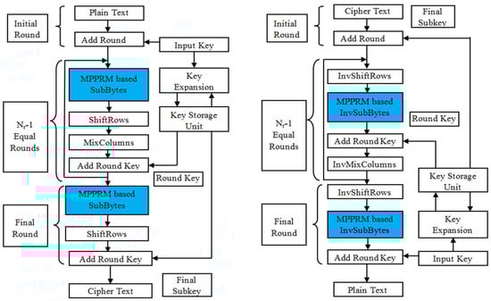
Figure 3.
Description of AES-128 encryption and decryption operations.
The encryption and decryption process of the AES-MPPRM architecture is similar to the conventional AES method. Here, the encryption/decryption data path includes an individual block. The processes accomplished in the encryption and decryption of AES-MPPRM architecture are Sub Byte/Inv-Sub Byte, Shift Row/Inv-Shift Row, Mix Column/Inv-Mix Column and Add Round Key. The steps carried out in the AES-MPPRM architecture is given as follows:
- Initially, the proposed MPPRM based Sub Byte transformation is performed the non-linear transformation over an individual byte of input state. The MPPRM is designed for minimizing the hardware utilization by reducing the logical operations carried out during the Sub Byte transformation.
- In second step of encryption, the circular shift through an individual bit is accomplished by using the shift row’s function.
- Each column of the state matrix is processed under the mix column operation. In that, every byte in each column is represented as a new value.
- Finally, the operation of XOR is performed over the current state matrix’s bytes along with the round key bytes to obtain the encryption output.
Composite field arithmetic architecture for the subbyte transformation is efficient in terms of power consumption, but power consumption can still be reduced by carefully designing some components of the CFA structure into two level logic architecture which is suitable for subpipelining architecture. Subbyte transformation operation can be splitted into three stages (pre-inversion stage, inversion stage, and post-inversion stage) to achieve better power efficiency. Splitting the subbyte transformation into further more stages increase the power consumption rather than decreasing it. Splitting the entire architecture into two stages also does not show any significance in power consumption. So it is wise to divide the CFA architecture for Subbyte and Invsubbyte transformation into three stages. All these stages are implemented with AND and XOR gate Arrays.
3.1. Modified PPRM Architecture
In AES-MPPRM architecture, the MPPRM is designed for the SubByte Transformation. Conventionally, the SubByte Transformation is implemented with three stage PPRM architecture as shown in Figure 4. PPRM architecture is modified into MPPRM with reduced area and improved time efficiency, by introducing a minute change in the second stage of PPRM architecture. In this MPPRM modification is introduced only in second stage, without altering any structural logic in stage-1 and stage-3. The sample modified architecture from the PPRM to the MPPRM is shown in Figure 5.
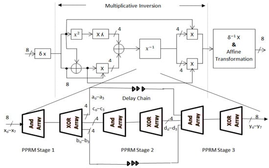
Figure 4.
PRRM based SubByte transformation.
Figure 5.
Sample structure for MPPRM architecture.
Figure 5 details the modification introduced in the stage-2 of standard PPRM architecture. By analyzing the above two logic structures, it is clear that new architecture has two EXOR gates and a single AND gate whereas the existing architecture has three EXOR gates and four AND gates. Output of both the architectures remains same irrespective of the gate used. A delay element has to be added to the output of AND gate in the second structure, since the processing time of AND gate is faster than the XOR gate. Main aim of PPRM architecture is to reduce the power consumption due to dynamic hazards is preserved in this new logical structure also. The logical expression of Figure 5 can be expressed as follows in Equation (6).
The difference between the conventional PPRM and MPPRM are clearly represented by using the mathematical expressions which are given in the following sections.
3.1.1. Mathematical Derivation for PPRM Architecture
The steps processed under the PPRM architecture are stated as follows:
Initially, an 8-bit input value is given as a input to the stage 1. In stage 1, the 8-bit input value is processed under AND and XOR arrays. Three different 4-bit output values such as & are taken from the input . The 4-bit values of & are expressed in Equations (7)–(9) respectively.
From the three 4-bit values of stage-1, the value of is taken as input for stage-2. Similar to stage-1, stage-2 is also processed with AND and XOR arrays. This stage-2 provides the one 4-bit value i.e., as shown in the Equation (10).
This stage-3 receives three 4-bit values as input & from the stage-1 and stage-2. Similar to the stage-1 and stage-2, stage-3 also processed with AND and XOR arrays. Further, this stage-3 provides the 8-bit output as shown in Equation (11).
3.1.2. Mathematical Derivation for MPPRM Architecture
In MPPRM architecture, stage-2 and stage-3 are similar to the PRRM architecture. Here, the modification is done only at the stage-1. Therefore, the calculation of and is remains unchanged as that PPRM architecture. The calculation process of is different than the PPRM architecture as shown in the Equation (12).
The architectural difference from PPRM to MPPRM for calculating the value in the stage-1 is shown in the Figure 6.
Figure 6.
Architectural diagram, (a) PPRM architecture and (b) MPPRM architecture.
From Figure 6, it is known that the PPRM structure requires 17 AND gates and 16 XOR gates whereas the MPPRM requires only 6 AND gates and 13 XOR gates. Therefore, the changes proposed in the stage-1 are used to reduce the hardware utilization of the MPPRM architecture. Meanwhile, the operating frequency of the AES-MPPRM architecture is minimized by increasing the speed of the overall AES architecture.
4. Detailed Hardware Implementation Architectures
Optimized architectures for all the stages of AES encryption and decryption are presented in detailed nature which increases speed and reduce the total area occupied by the existing architecture. An efficient key expansion, mixcolumn and invmixcolumn structure is also provided in this section.
4.1. Subbytes/Invsubbytes Transformation
In Subbyte and Invsubbyte transformation stage, multiplicative inversion operation takes a large number of gates to give the correct output. It takes approximately 620 gates to find the multiplicative inverse in GF(28). As it is known that multiplicative inverse in GF(28) can be found out in GF((24)2), then it can be decomposed into GF(22) and then finally into GF(2). Multiplicative inverse in GF(2) is a simple logical AND operation. An efficient method to find the multiplicative inverse is to find the inverse of each bit i.e., {y3, y2, y1, y0} = {y3−1, y2−1, y1−1, y0−1}. It is illustrated in the following Equation (13).
Multiplicative inverse found from the above equation requires only 14 XOR gates and 9 AND gates only. Three XOR gates and two AND gates are in the critical path. This architecture can be shared by encryption and decryption operation if both the operations are to be implemented in the same device.
4.2. Mixcolumns/Invmixcolumns
Since subpipelining is employed in subbyte transformation, a suitable architecture for the mixcolumn and inverse mixcolumn that shares common structure is proposed. In mixcolumn transformation it is essential to calculate multiplication of 02 and 03 operations. Generally, mixcolumn operation is modified as shown in Equation (14).
where .
By the above expressions, 03 multiplications are avoided and the following Figure 7 shows the 02 multiplication process in GF.
Figure 7.
Multiplication process of 02 in GF.
From the above Figure 7, it is clear that 02 multiplications in GF can be implemented with only 3 XOR gates. Like mixcolum, invmixcolumn structure can also be modified to a structure that suits better for subpipelining architecture. Matrix used in the inverse mixcolumn is rewritten as shown in Equation (15).
In the invmixcolumn, it is enough to find the multiplication operations of 02 and 04. 04 can multiplication can be computed by cascading 02 multiplication process or by the process shown in the following Figure 8.
Figure 8.
Multiplication process of 04 in GF.
From the above structure, 5 XOR gates are needed to implement 04 multiplications. From equation it is clear that it is possible to implement invmixcolumn by adding some extra logics with the mixcolumn structure. Therefore, the same architecture can be shared with mixcolumn and inverse mixcolumn operations.
5. Results and Discussion
The proposed fully subpipelined AES architecture for 128-bit key is implemented on Xilinx FPGA. For synthesis, timing, and power analysis, Xilinx ISE 5.1 is used. For each clock cycle, data blocks of 128 bits are accepted in the fully subpipelined encryptor. Next, a 128-bit output data is taken for each input block as the cipher text in an each clock cycle. A hardware description language (HDL) is used to design and implement the AES-MPPRM architecture. The designed AES-MPPRM architecture is used to process the 128 bit of cryptography.
5.1. Performance Analysis
The performance of the AES-MPPRM architecture is analyzed in five different FPGA devices such as Kintex 7, Spartan 3, Spartan 6, Virtex 5, and Virtex 6. The performances of the AES-MPPRM architecture are analyzed in terms of number of slice registers, flip flops, number of slice LUTs, number of logical elements, slices, bonded IOB, operating frequency, and delay. Moreover, the performance of the proposed AES-MPPRM architecture is analyzed with the AES-PPRM architecture.
Table 3, Table 4 and Table 5 shows the hardware utilization analysis for the AES-MPPRM architecture of Kintex 7, Spartan 3, Spartan 6, Virtex 5, and Virtex 6 FPGA devices. Additionally, the frequency and delay analysis of the AES-MPPRM architecture is given in Table 6. Here, the results of the AES-MPPRM architecture are evaluated with the AES-PPRM architecture. The results of the AES-MPPRM architecture for the encryption and decryption processes are taken for the 128-bit of cryptography. The LUT, slices, and flip flops for the AES-MPPRM architecture designed in the Spartan 6 FPGA device are 197, 79, and 88, which are less when compared to the AES-PPRM architecture. From the performance analysis, it is concluded that the AES-MPPRM architecture achieves the better performance than the AES-PPRM architecture. The reason for the AES-PPRM architecture with higher hardware resource utilization is that it used high amount of AND and XOR gates during the Sub Bytes transformation. However, the AES-MPPRM architecture uses only less amount of AND and XOR gates in the Sub Bytes transformation. More specifically, the AES-MPPRM architecture designed in the Kintex 7, Spartan 3, Spartan 6, Virtex 5, and Virtex 6 FPGA devices consumes only less than or equal to the 70% of resources. Therefore, the proposed AES-MPPRM architecture consumes less hardware resources based on the MPPRM Sub Bytes transformation and its subpipelinining architecture.
Table 3.
Hardware utilization analysis of AES-MPPRM for Kintex 7 FPGA device.
Table 4.
Hardware utilization analysis of AES-MPPRM for Spartan FPGA devices.
Table 5.
Hardware utilization analysis of AES-MPPRM for Virtex FPGA devices.
Table 6.
Analysis of operating frequency and delay for AES-MPPRM.
5.2. Comparative Analysis
This section shows the comparative analysis of the AES-MPPRM architecture with existing AES architectures. There are five AES architectures, including LAES [47], AES-CTR [48], AES-CFA [49], AES-BSRD [50], and AES-EMCBE [51], which are used to justify the effectiveness of the AES-MPPRM architecture. The comparison between the AES-MPPRM with existing AES architectures are given as follows:
The comparison of the AES-MPPRM architecture with LAES [47], AES-CTR [48], AES-CFA [49], AES-BSRD [50], and AES-EMCBE [51] is shown in Table 7, Table 8, Table 9, Table 10, Table 11, respectively. Additionally, the LUT comparison graph among the existing AES architectures and AES-MPPRM is presented in Figure 9. From the analysis, it is concluded that the AES-MPPRM architecture outperforms well than the LAES [47], AES-CTR [48], AES-CFA [49], AES-BSRD [50], and AES-EMCBE [51]. For example, the number of slice LUT is 197 for the AES-MPPRM with Spartan 6 FPGA, and it is even less when compared to the AES-BSRD [50]. The area of AES-BSRD [50] is increased due to its replication of linear operation during the encryption/decryption process. The hardware utilization of the AES-MPPRM architecture is reduced mainly due to the fact that it doesn’t depend on the LUT while designing the SubBytes and InvSubBytes stages. Here, the combinational logical circuit is used to design the SubBytes and InvSubBytes transformation. The MPPRM structure is used to minimize the hardware utilization during the encryption and decryption processes. Here, the combination of the subpipelining structure with MPPRM structure is used to minimize the delay.
Table 7.
Comparison of AES-MPPRM and LAES for Kintex 7 FPGA.
Table 8.
Comparison of AES-MPPRM and AES-CTR for Virtex 5 FPGA.
Table 9.
Comparison of AES-MPPRM and AES-CFA for Spartan 3 FPGA.
Table 10.
Comparison of AES-MPPRM and AES-BSRD for Spartan 6 FPGA.
Table 11.
Comparison of AES-MPPRM and AES-EMCBE for Virtex 6 FPGA.
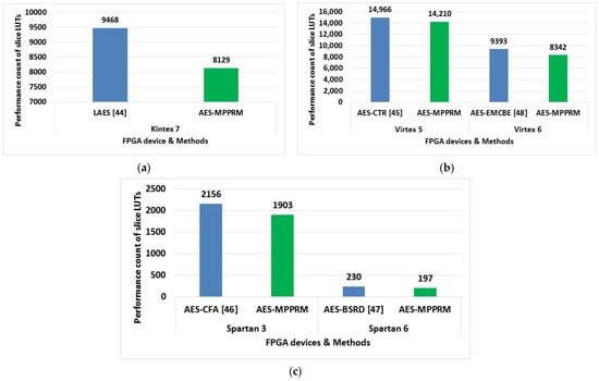
Figure 9.
Comparison of slice LUTs for the AES-MPPRM and existing AES architectures. (a) Kintex FPGA device, (b) Virtex FPGA devices, (c) Spartan FPGA devices.
5.3. Case Study
Cryptographic Process on X-ray Image of a Disjoint in Human Shoulder
This AES-MPPRM architecture is implemented for the secure transmission of the human shoulder X-ray image. This secure transmission happens as an image encryption and decryption using modified AES algorithm.
In the image encryption, pixel value of the X-ray image which is to be transmitted securely is obtained with the MATLAB 6.5 programming software. These pixel values act as one of the input data to the proposed AES algorithm. The input data can be from 0 to 255 (i.e., Pixel value) and the input pixel values are . Figure 10 shows the input and histogram image, where the input pixel values are converted into binary form using the command of . Subsequently, these binary data are given as the input and it is encrypted using the AES-MPPRM architecture. The output is taken in the form of hexadecimal values which is in 8-bit. The encrypted values from the AES-MPPRM architecture are . The output of this algorithm is the cipher text values which can be transmitted across the world securely. With this cipher text value, unauthorized persons cannot obtain the original information without knowledge of the secret key. The encrypted image and its histogram are shown in the Figure 11. At the receiving end, obtained cipher text values are once again converted back into pixel values of the original images by the using the same proposed architecture. Then this same process is used for all the pixel values of the image. Then these pixel values are used by MATLAB to produce the original image at the receiver end.
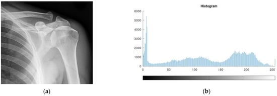
Figure 10.
Input image: (a) X-ray image and (b) histogram.
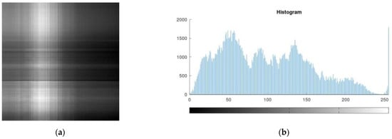
Figure 11.
Output image: (a) Encrypted Image and (b) Histogram.
Decrypted image is obtained with the MATLAB by the process of converting encrypted pixel values to the images. From the encrypted results and histogram images, it is clear that the AES-MPPRM architecture achieves higher security.
6. Conclusions
In this paper, the SubBytes/InvSubBytes transformation of the AES architecture was designed using the MPPRM structure. Subsequently, the designed SubBytes/InvSubBytes transformation was used to develop an effective subpipelining architecture. This same subpipeline architecture can be implemented for other versions of the AES such as AES-192 and AES-256 algorithms, by making slight modifications in the key expansion unit. Hence, the MPPRM architecture used in the AES helped to reduce the amount of hardware resources. Moreover, the delay of the overall circuit was minimized using the integration of subpipelining and MPPRM structure. Accordingly, the lesser delay leads to the higher operating frequency for the AES-MPPRM architecture. The LUT of the AES-MPPRM architecture designed in the Spartan 6 is 197, which is much less compared to the AES-BSRD. In future, the modified key expansion architecture can be developed for minimizing the time consumption during the key generation. It can also be extended by employing the cryptanalysis process to check the security of the algorithm by introducing some attacks (such as a side channel attack).
Author Contributions
The paper investigation, resources, data curation, writing—original draft preparation, writing—review and editing, and visualization were undertaken by T.M.K. and K.S.R. The paper conceptualization, software, validation, formal analysis, methodology were done by K.A. Supervision, project administration, and final approval of the version to be published were conducted by S.R. and B.D.P. All authors have read and agreed to the published version of the manuscript.
Funding
This research received no external funding.
Institutional Review Board Statement
Not applicable.
Informed Consent Statement
Not applicable.
Data Availability Statement
No new data were created or analyzed in this study. Data sharing is not applicable to this article.
Conflicts of Interest
The authors declare no conflict of interest.
References
- Rahimunnisa, K.; Karthigaikumar, P.; Rasheed, S.; Jayakumar, J.; Sureshkumar, S. FPGA implementation of AES algorithm for high throughput using folded parallel architecture. Secur. Commun. Netw. 2012, 7, 2225–2236. [Google Scholar] [CrossRef]
- Farooq, U.; Aslam, M.F. Comparative analysis of different AES implementation techniques for efficient resource usage and better performance of an FPGA. J. King Saud Univ. Comput. Inf. Sci. 2017, 29, 295–302. [Google Scholar] [CrossRef]
- Rajasekar, P.; Mangalam, H. Efficient FPGA implementation of AES 128 bit for IEEE 802.16e mobile WiMax standards. Circuits Syst. 2016, 07, 371–380. [Google Scholar] [CrossRef][Green Version]
- Zeebaree, S.R.M. DES encryption and decryption algorithm implementation based on FPGA. Indones. J. Electr. Eng. Comput. Sci. 2020, 18, 774–781. [Google Scholar] [CrossRef]
- Ferrari, P.; Sisinni, E.; Bellagente, P.; Rinaldi, S.; Pasetti, M.; de Sa, A.O.; Machado, R.C.S.; Carmo, L.F.R.D.C.; Casimiro, A. Model-Based Stealth Attack to Networked Control System Based on Real-Time Ethernet. IEEE Trans. Ind. Electron. 2021, 68, 7672–7683. [Google Scholar] [CrossRef]
- Kumar, T.M.; Karthigaikumar, P. FPGA implementation of an optimized key expansion module of AES algorithm for secure transmission of personal ECG signals. Des. Autom. Embed. Syst. 2018, 22, 13–24. [Google Scholar] [CrossRef]
- Kumar, P.K.; Baskaran, K. An ASIC implementation of low power and high throughput blowfish crypto algorithm. Microelectron. J. 2010, 41, 347–355. [Google Scholar] [CrossRef]
- Visconti, P.; Capoccia, S.; Venere, E.; Velázquez, R.; Fazio, R.D. 10 Clock-Periods Pipelined Implementation of AES-128 Encryption-Decryption Algorithm up to 28 Gbit/s Real Throughput by Xilinx Zynq UltraScale+ MPSoC ZCU102 Platform. Electronics 2020, 9, 1665. [Google Scholar] [CrossRef]
- Priya, S.S.; Karthigaikumar, P.; Mangai, N.M.S.; Das, P.K.G. An Efficient Hardware Architecture for High Throughput AES Encryptor Using MUX Based Sub Pipelined S-Box. Wirel. Pers. Commun. 2017, 94, 2259–2273. [Google Scholar] [CrossRef]
- Mohd, B.J.; Hayajneh, T.; Abu Khalaf, Z.; Yousef, K.A. Modeling and optimization of the lightweight HIGHT block cipher design with FPGA implementation. Secur. Commun. Netw. 2016, 9, 2200–2216. [Google Scholar] [CrossRef]
- Dofe, J.; Pahlevanzadeh, H.; Yu, Q. A Comprehensive FPGA-Based Assessment on Fault-Resistant AES against Correlation Power Analysis Attack. J. Electron. Test. 2016, 32, 611–624. [Google Scholar] [CrossRef]
- Della Giustina, D.; Rinaldi, S.; Robustelli, S.; Angioni, A. Massive Generation of Customer Load Profiles for Large Scale State Estimation Deployment: An Approach to Exploit AMI Limited Data. Energies 2021, 14, 1277. [Google Scholar] [CrossRef]
- Dede, A.; Della Giustina, D.; Rinaldi, S.; Ferrari, P.; Flammini, A.; Vezzoli, A. Smart meters as part of a sensor network for monitoring the low voltage grid. 2015 IEEE Sens. Appl. Symp. SAS 2015, 1–6. [Google Scholar] [CrossRef]
- Abdulazeez, A.M.; Tahir, A.S. Design and Implementation of Advanced Encryption Standard Security Algorithm using FPGA. Int. J. Comput. Technol. 2013, 4, 1988–1993. [Google Scholar]
- Mestiri, H.; Kahri, F.; Bouallegue, B.; Machhout, M. A high-speed AES design resistant to fault injection attacks. Microprocess. Microsyst. 2016, 41, 47–55. [Google Scholar] [CrossRef]
- Shahbazi, K.; Ko, S.-B. Area-Efficient Nano-AES Implementation for Internet-of-Things Devices. IEEE Trans. Very Large Scale Integr. VLSI Syst. 2021, 29, 136–148. [Google Scholar] [CrossRef]
- Kundi, D.-S.; Aziz, A.; Ikram, N. A high performance ST-Box based unified AES encryption/decryption architecture on FPGA. Microprocess. Microsyst. 2016, 41, 37–46. [Google Scholar] [CrossRef]
- Soltani, A.; Sharifian, S. An ultra-high throughput and fully pipelined implementation of AES algorithm on FPGA. Microprocess. Microsystems 2015, 39, 480–493. [Google Scholar] [CrossRef]
- Rahimunnisa, K.; Karthigaikumar, P.; Christy, N.A.; Kumar, S.S.; Jayakumar, J. PSP: Parallel sub-pipelined architecture for high throughput AES on FPGA and ASIC. Open Comput. Sci. 2013, 3, 173–186. [Google Scholar] [CrossRef]
- De Meyer, L.; Moradi, A.; Wegener, F. Spin Me Right Round Rotational Symmetry for FPGA-Specific AES. IACR Trans. Cryptogr. Hardw. Embed. Syst. 2018, 596–626. [Google Scholar] [CrossRef]
- Rekha, S.S.; Saravanan, P. Low-Cost AES-128 Implementation for Edge Devices in IoT Applications. J. Circuits, Syst. Comput. 2019, 28, 1950062. [Google Scholar] [CrossRef]
- Parmar, N.D.; Kadam, P. High speed architecture implementation of AES using FPGA. Int. J. Comput. Appl. 2015, 975, 8887. [Google Scholar]
- Kalaiselvi, K.; Mangalam, H. Power efficient and high performance VLSI architecture for AES algorithm. J. Electr. Syst. Inf. Technol. 2015, 2, 178–183. [Google Scholar] [CrossRef][Green Version]
- Chellam, M.B.; Natarajan, R. AES Hardware Accelerator on FPGA with Improved Throughput and Resource Efficiency. Arab. J. Sci. Eng. 2018, 43, 6873–6890. [Google Scholar] [CrossRef]
- Farashahi, R.R.; Rashidi, B.; Sayedi, S.M. FPGA based fast and high-throughput 2-slow retiming 128-bit AES encryption al-gorithm. Microelectron. J. 2014, 45, 1014–1025. [Google Scholar] [CrossRef]
- Ibrahim, A. FPGA-based Hardware Implementation of Compact AES Encryption Hardware Core. WSEAS Trans. Circuits Syst. 2015, 14, 365–372. [Google Scholar]
- Khan, F.H.; Shams, R.; Hasan, A.; Hasan, N. Implementation of Data Encryption Standard (DES) on FPGA. J. Inf. Commun. Technol. Robot. Appl. 2018, 5, 47–59. [Google Scholar]
- Thind, V.; Pandey, B.; Kalia, K.; Hussain, D.A.; Das, T.; Kumar, T. FPGA based low power DES algorithm design and im-plementation using HTML technology. Int. J. Softw. Eng. Appl. 2016, 10, 81–92. [Google Scholar]
- Oukili, S.; Bri, S. High throughput FPGA Implementation of Data Encryption Standard with time variable sub-keys. Int. J. Electr. Comput. Eng. 2016, 6, 298. [Google Scholar]
- Del Rosal, E.; Kumar, S. A Fast FPGA Implementation for Triple DES Encryption Scheme. Circuits Syst. 2017, 08, 237–246. [Google Scholar] [CrossRef]
- Kumar, N.P.; Shirisha, C. An area-efficient ECC architecture over GF (2m) for resource-constrained applications. AEU Int. J. Electr. Commun. 2020, 125, 153383. [Google Scholar] [CrossRef]
- Realpe-Muñoz, P.C.; Velasco-Medina, J. High-performance elliptic curve cryptoprocessors over GF (2m) on Koblitz curves. Analog Integr. Circuits Signal Process. 2015, 85, 129–138. [Google Scholar] [CrossRef]
- Wu, T.; Wang, R. Fast unified elliptic curve point multiplication for NIST prime curves on FPGAs. J. Cryptogr. Eng. 2019, 9, 401–410. [Google Scholar] [CrossRef]
- Parrilla, L.; Álvarez-Bermejo, J.A.; Castillo, E.; López-Ramos, J.A.; Morales-Santos, D.P.; García, A. Elliptic Curve Cryptog-raphy hardware accelerator for high-performance secure servers. J. Supercomput. 2019, 75, 1107–1122. [Google Scholar] [CrossRef]
- Kalia, J.; Mittal, V. Performance Enhancement of the RSA Algorithm by Optimize Partial Product of Booth Multiplier. Int. J. Electron. Eng. Res. 2017, 9, 1329–1338. [Google Scholar]
- García, R.; Algredo-Badillo, I.; Morales-Sandoval, M.; Feregrino-Uribe, C.; Cumplido, R. A compact FPGA-based processor for the Secure Hash Algorithm SHA-256. Comput. Electr. Eng. 2014, 40, 194–202. [Google Scholar] [CrossRef]
- El-Maksoud, A.J.A.; El-Kader, A.A.A.; Hassan, B.G.; Rihan, N.G.; Tolba, M.; Said, L.A.; Radwan, A.G.; Abu-Elyazeed, M.F. FPGA implementation of sound encryption system based on fractional-order chaotic systems. Microelectron. J. 2019, 90, 323–335. [Google Scholar] [CrossRef]
- Abed, S.; Jaffal, R.; Mohd, B.J.; Alshayeji, M. FPGA Modeling and Optimization of a SIMON Lightweight Block Cipher. Sensors 2019, 19, 913. [Google Scholar] [CrossRef] [PubMed]
- Pirpilidis, F.; Pyrgas, L.; Kitsos, P. 8-bit serialised architecture of SEED block cipher for constrained devices. IET Circuits Devices Syst. 2020, 14, 316–321. [Google Scholar] [CrossRef]
- Aghaie, A.; Kermani, M.M.; Azarderakhsh, R. Reliable and Fault Diagnosis Architectures for Hardware and Software-Efficient Block Cipher KLEIN Benchmarked on FPGA. IEEE Trans. Comput. Des. Integr. Circuits Syst. 2018, 37, 901–905. [Google Scholar] [CrossRef]
- Chen, H.; Wang, T.; Zhang, F.; Zhao, X.; He, W.; Xu, L.; Ma, Y. Stealthy Hardware Trojan Based Algebraic Fault Analysis of HIGHT Block Cipher. Secur. Commun. Netw. 2017, 2017, 1–15. [Google Scholar] [CrossRef]
- Wu, N.; Ali, Z.A.; Shaikh, M.M.; Yahya, M.R.; Aamir, M. Compact and High Speed Architectures of KASUMI Block Cipher. Wirel. Pers. Commun. 2019, 106, 1787–1800. [Google Scholar] [CrossRef]
- Rashidi, B. Efficient and flexible hardware structures of the 128 bit CLEFIA block cipher. IET Comput. Digit. Tech. 2020, 14, 69–79. [Google Scholar] [CrossRef]
- Pandey, J.G.; Goel, T.; Karmakar, A. Hardware architectures for PRESENT block cipher and their FPGA implementations. IET Circuits Devices Syst. 2019, 13, 958–969. [Google Scholar] [CrossRef]
- Lara-Nino, C.A.; Diaz-Perez, A.; Morales-Sandoval, M. Lightweight Hardware Architectures for the Present Cipher in FPGA. IEEE Trans. Circuits Syst. I Regul. Pap. 2017, 64, 2544–2555. [Google Scholar] [CrossRef]
- Kaedi, S.; Doostari, M.A.; Ghaznavi-Ghoushchi, M.B. Low-complexity and differential power analysis (DPA)-resistant two-folded power-aware Rivest–Shamir–Adleman (RSA) security schema implementation for IoT-connected devices. IET Comput. Digit. Tech. 2018, 12, 279–288. [Google Scholar] [CrossRef]
- Kumar, K.; Ramkumar, K.; Kaur, A. A Lightweight AES Algorithm Implementation for Encrypting Voice Messages using Field Programmable Gate Arrays. J. King Saud Univ. Comput. Inf. Sci. 2020. [Google Scholar] [CrossRef]
- Shahbazi, K.; Ko, S. High throughput and area-efficient FPGA implementation of AES for high-traffic applications. IET Comput. Digit. Tech. 2020, 14, 344–352. [Google Scholar] [CrossRef]
- Murugan, C.A.; Karthigaikumar, P.; Priya, S.S. FPGA implementation of hardware architecture with AES encryptor using sub-pipelined S-box techniques for compact applications. Automatika 2020, 61, 682–693. [Google Scholar] [CrossRef]
- Wegener, F.; De Meyer, L.; Moradi, A. Spin Me Right Round Rotational Symmetry for FPGA-Specific AES: Extended Version. J. Cryptol. 2020, 33, 1114–1155. [Google Scholar] [CrossRef]
- Madhavapandian, S.; Pandi, P.M. FPGA implementation of highly scalable AES algorithm using modified mix column with gate replacement technique for security application in TCP/IP. Microprocess. Microsystems 2019, 73, 102972. [Google Scholar] [CrossRef]
- Zodpe, H.; Sapkal, A. An efficient AES implementation using FPGA with enhanced security features. J. King Saud Univ. Eng. Sci. 2020, 32, 115–122. [Google Scholar] [CrossRef]
- Sikka, P.; Asati, A.; Shekhar, C. High-throughput field-programable gate array implementation of the advanced encryption standard algorithm for automotive security applications. J. Ambient. Intell. Humaniz. Comput. 2021, 12, 7273–7279. [Google Scholar] [CrossRef]
- Ahmad, R.; Kho, D.; Manaf, A.A.; Ismail, W. Parallel-Pipelined-Memory-Based Blowfish Design with Reduced FPGA Utili-zation for Secure ZigBee Real-Time Transmission. Wirel. Pers. Commun. 2019, 104, 471–489. [Google Scholar] [CrossRef]
Publisher’s Note: MDPI stays neutral with regard to jurisdictional claims in published maps and institutional affiliations. |
© 2021 by the authors. Licensee MDPI, Basel, Switzerland. This article is an open access article distributed under the terms and conditions of the Creative Commons Attribution (CC BY) license (https://creativecommons.org/licenses/by/4.0/).