
Influence of Parasitic Resistances on the Input Resistance of Buck and Boost Converters in Maximum Power Point Tracking (MPPT) Systems


Abstract
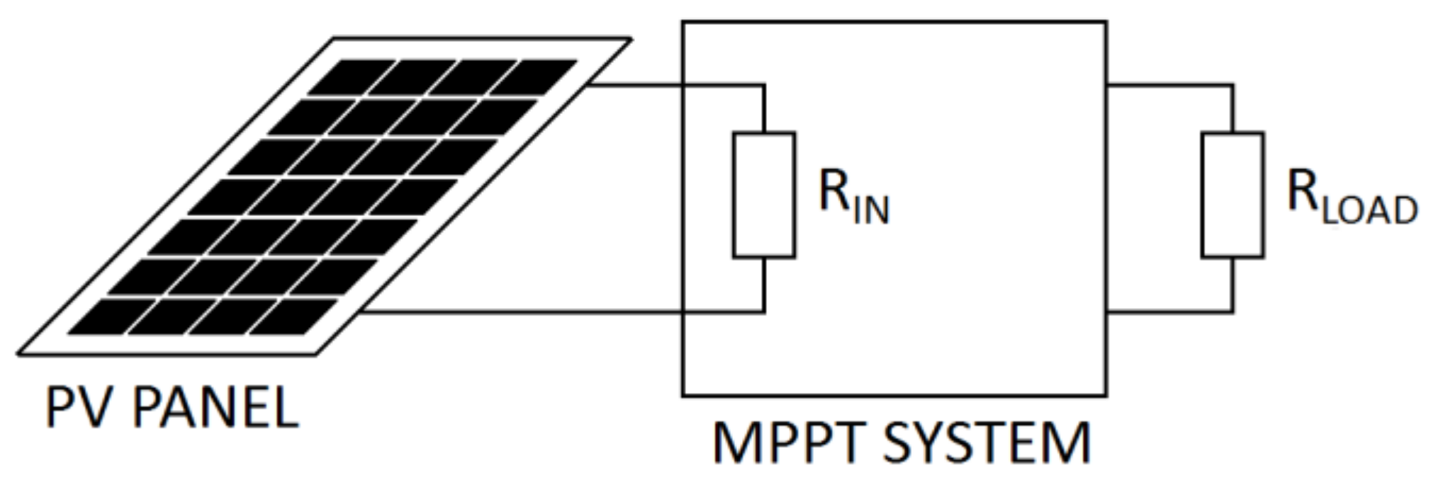
:1. Introduction
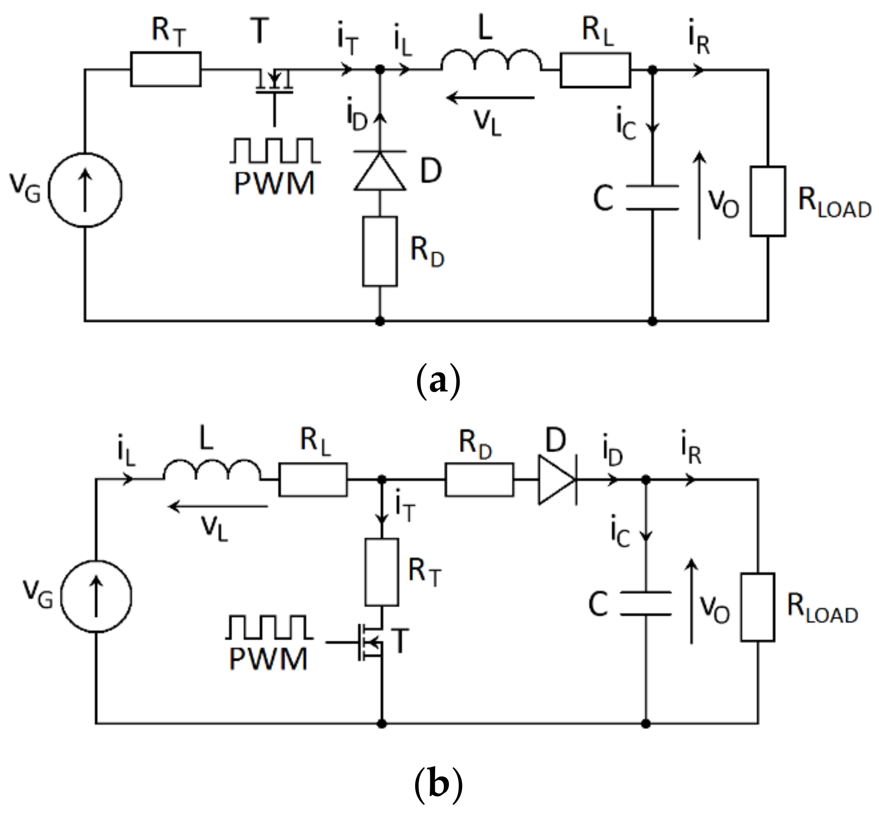
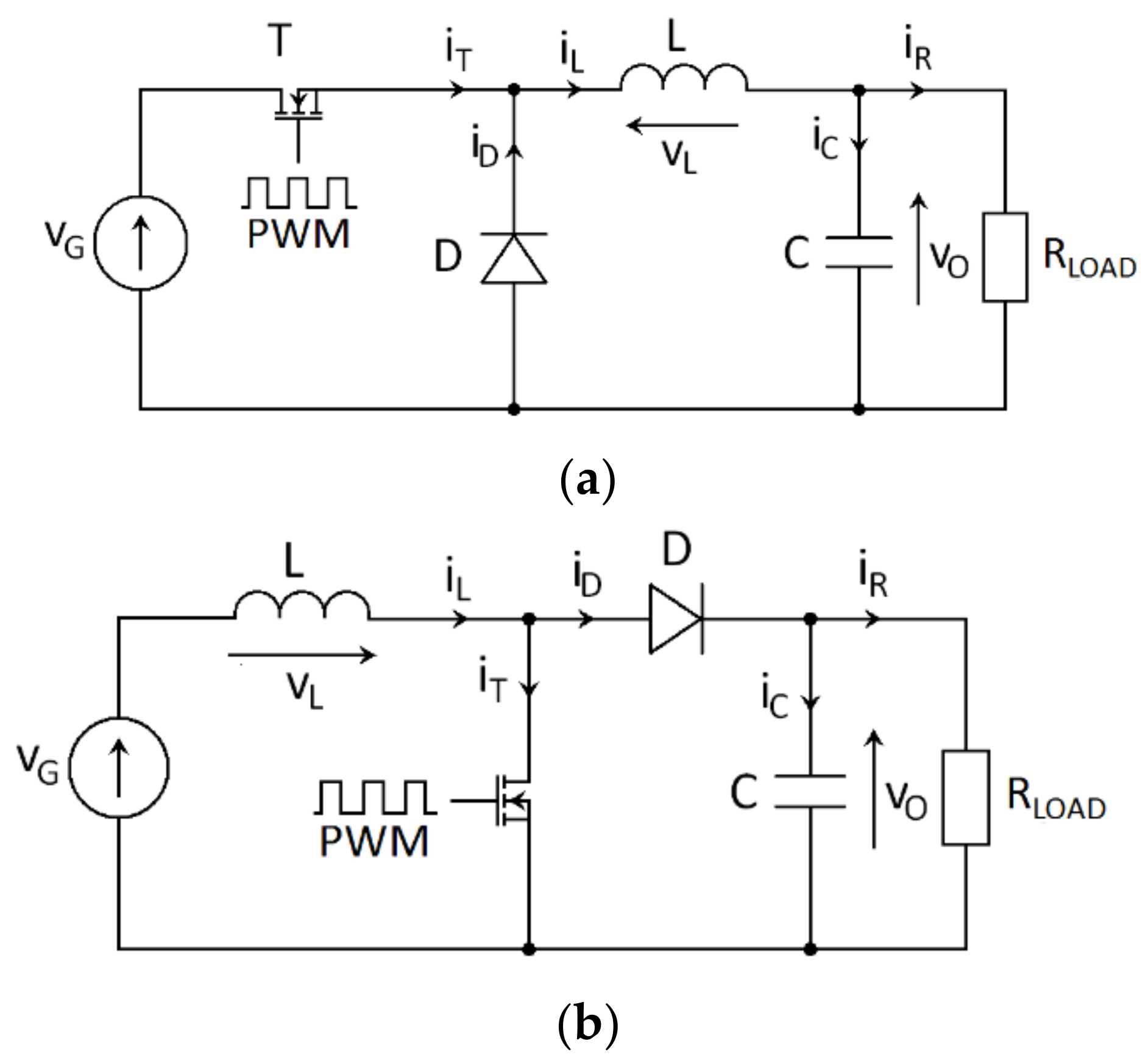
2. Parasitic Resistances in DC/DC Converters and Their Impact on Converter Input Resistance
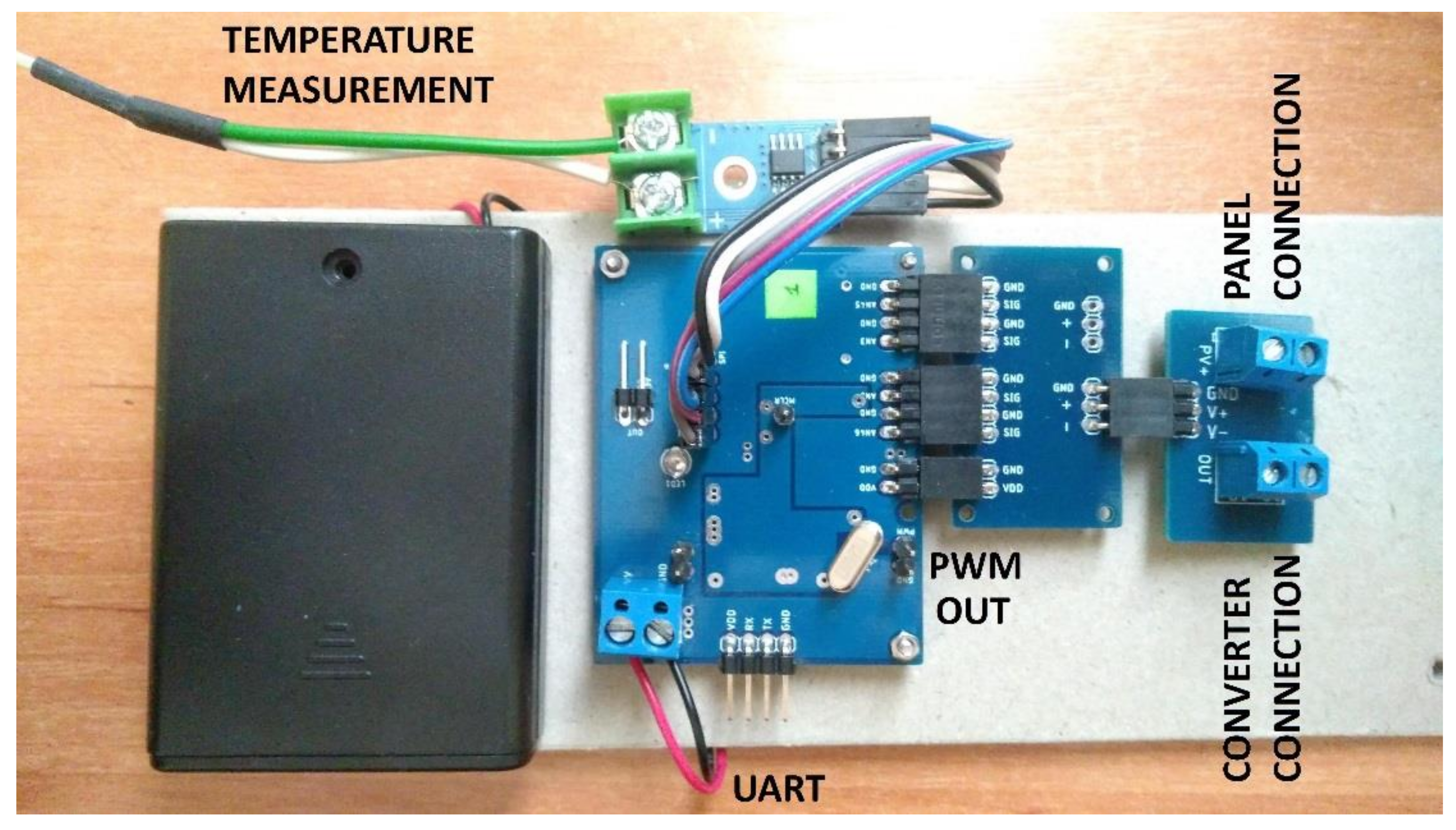
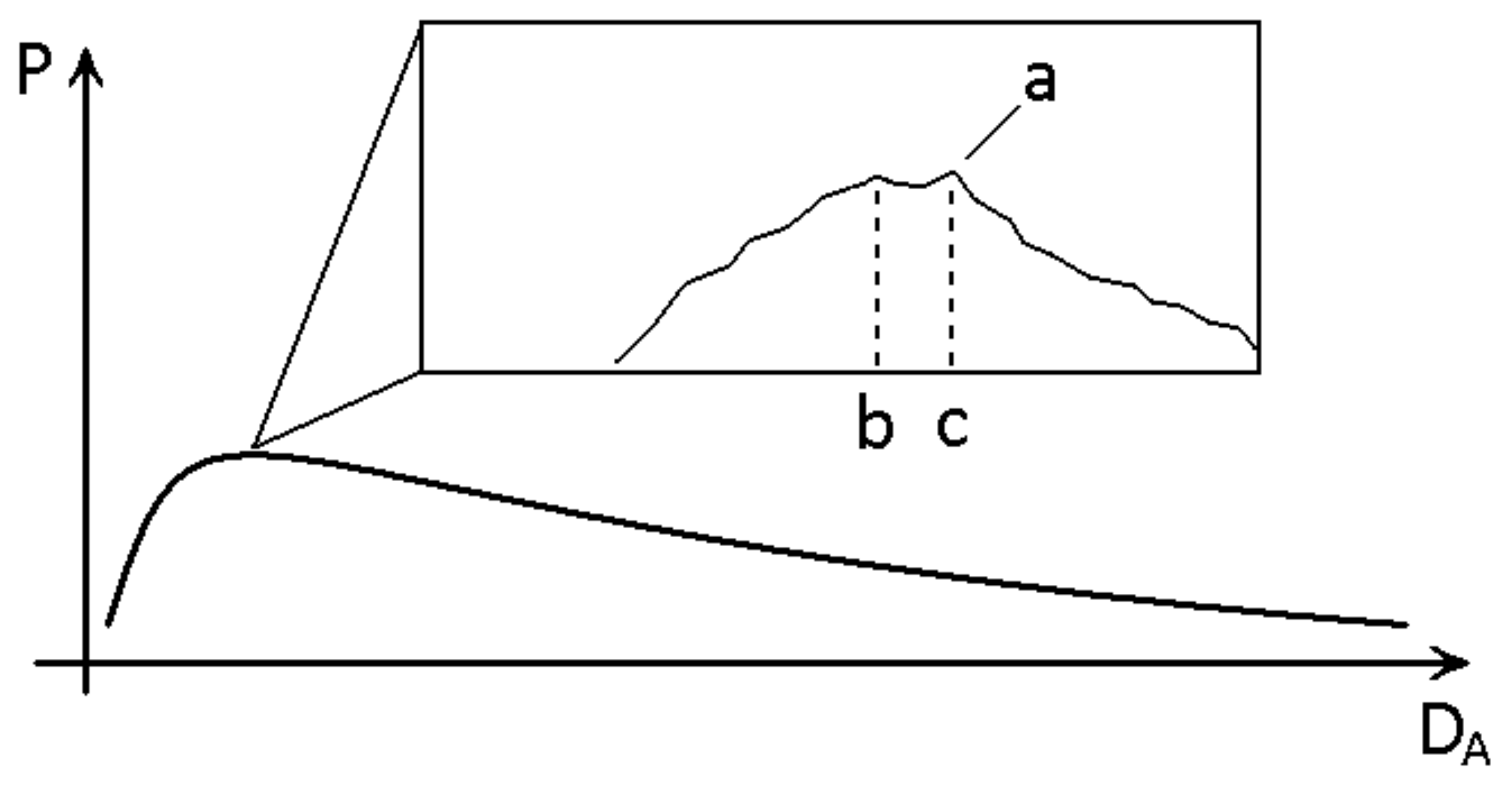
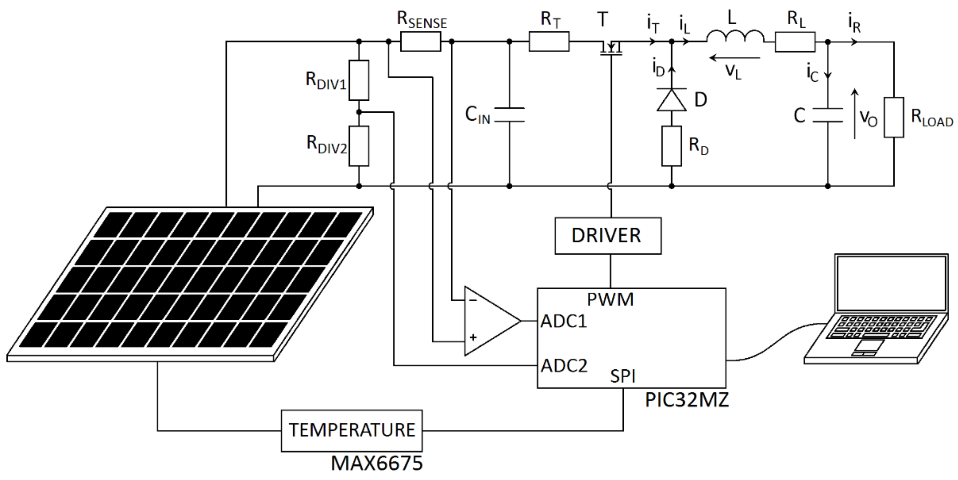
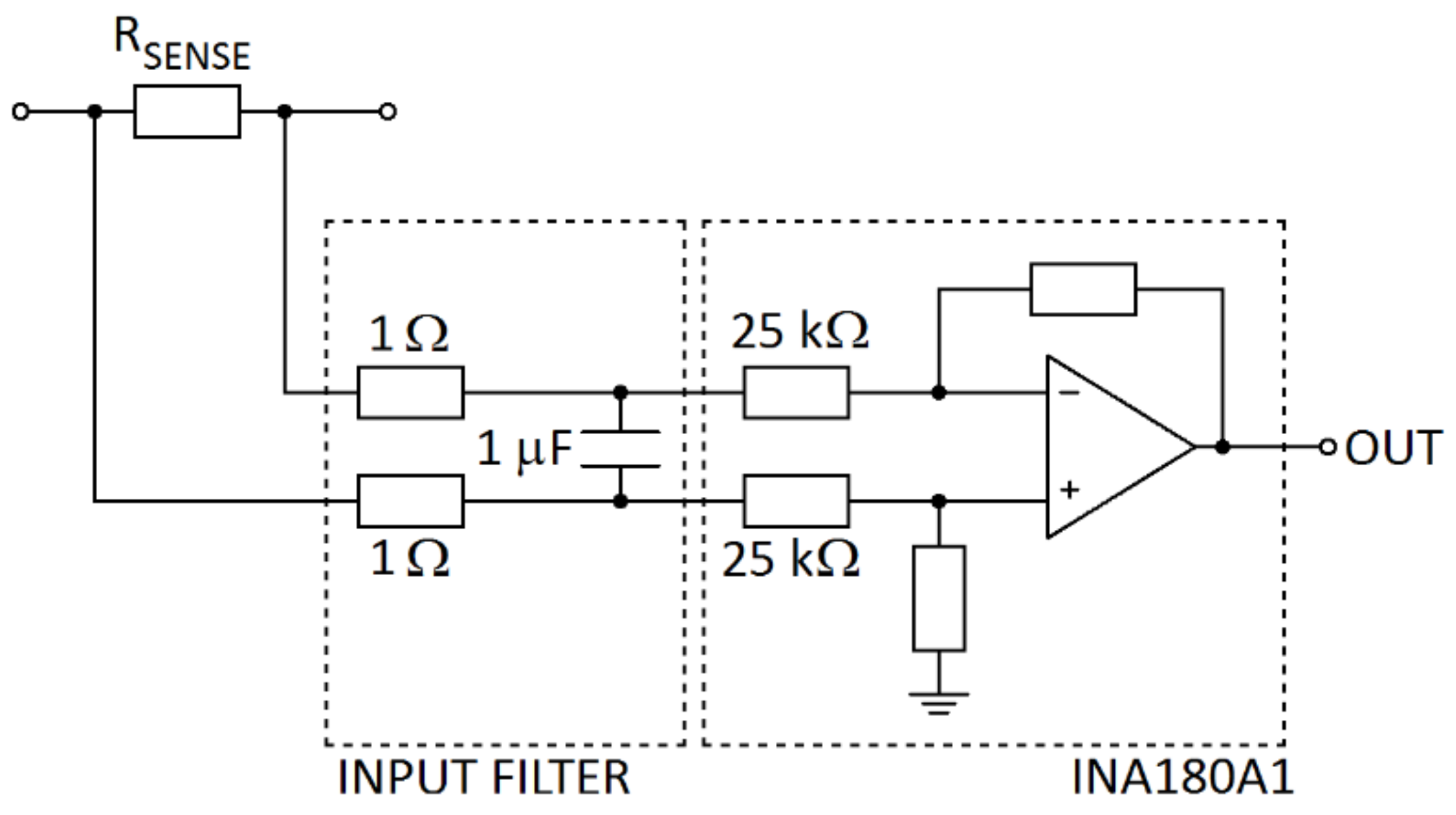
3. Materials and Methods
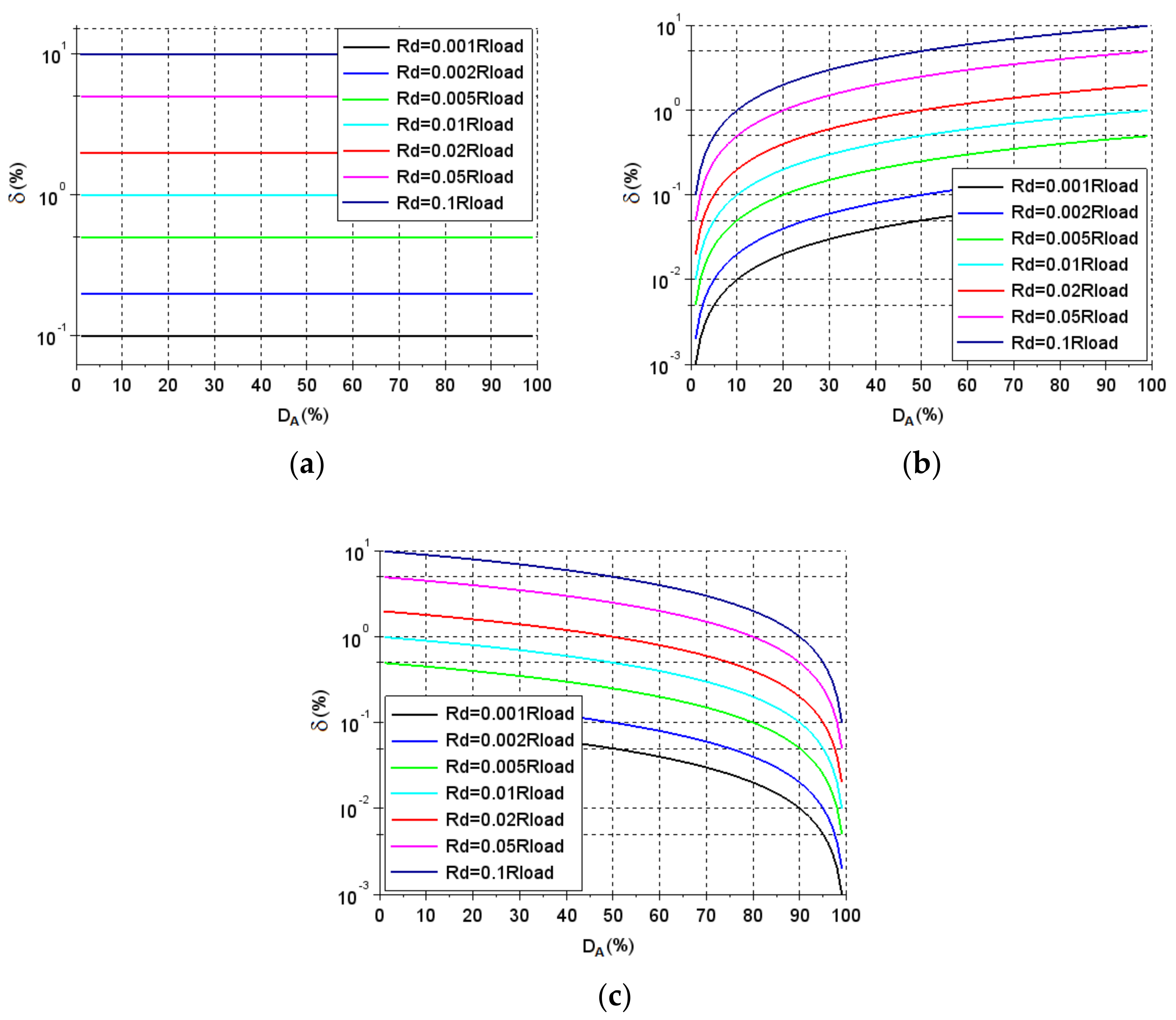
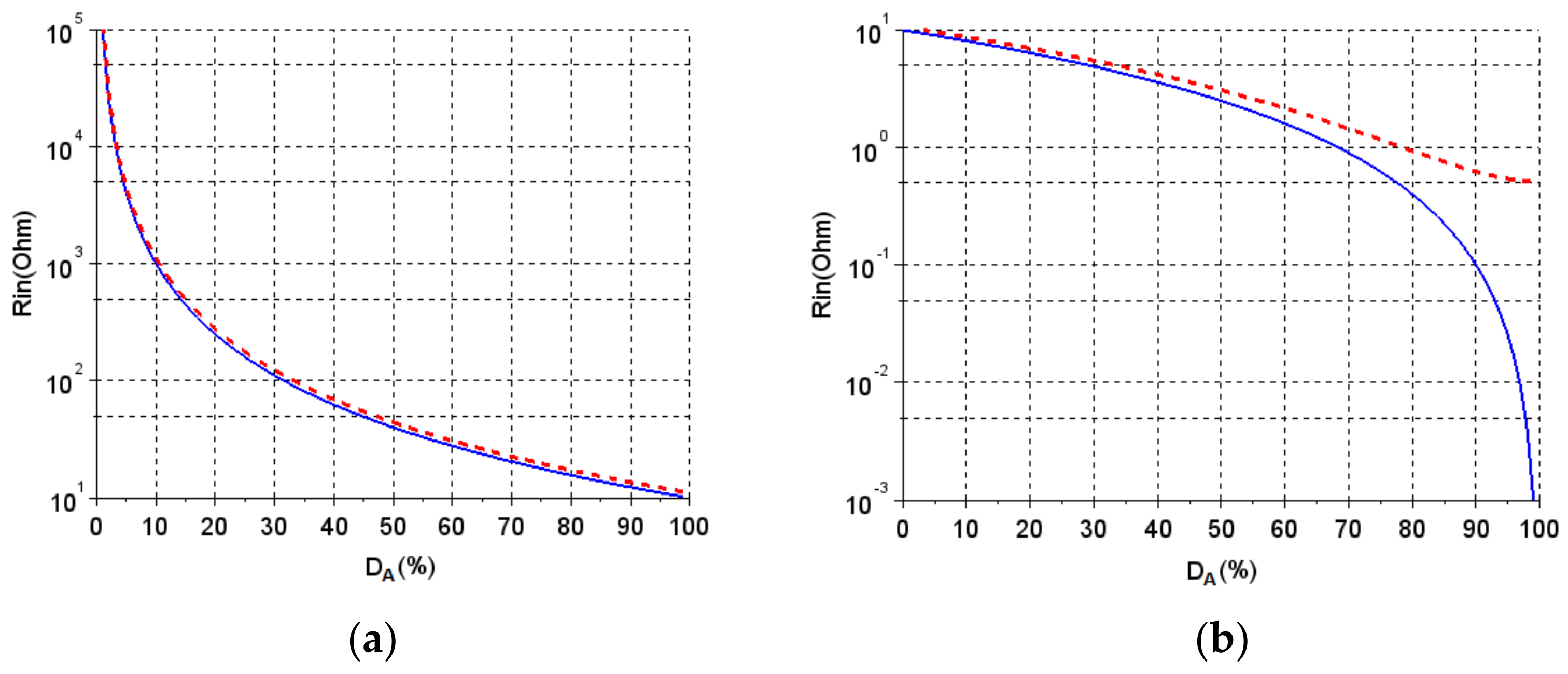
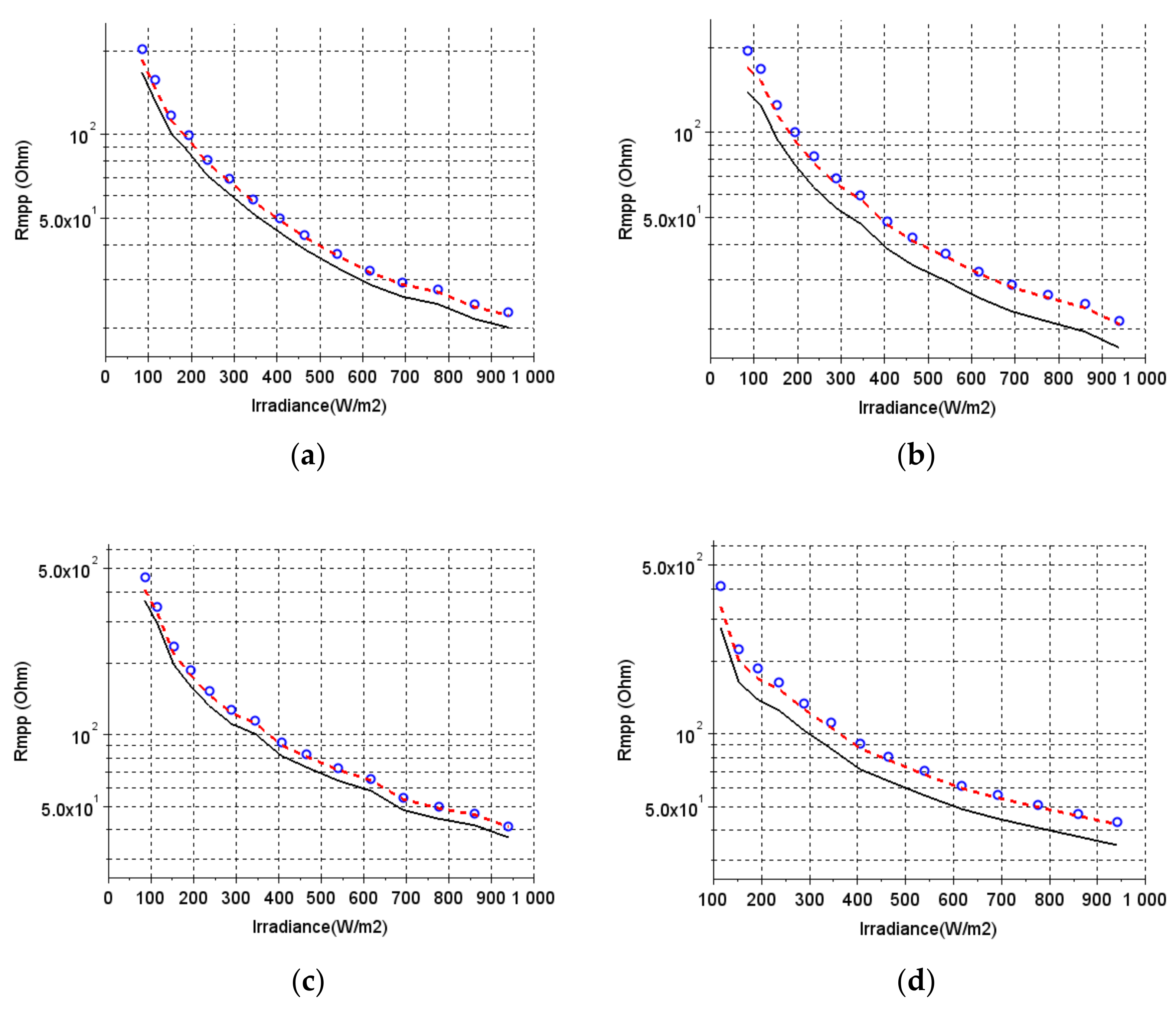
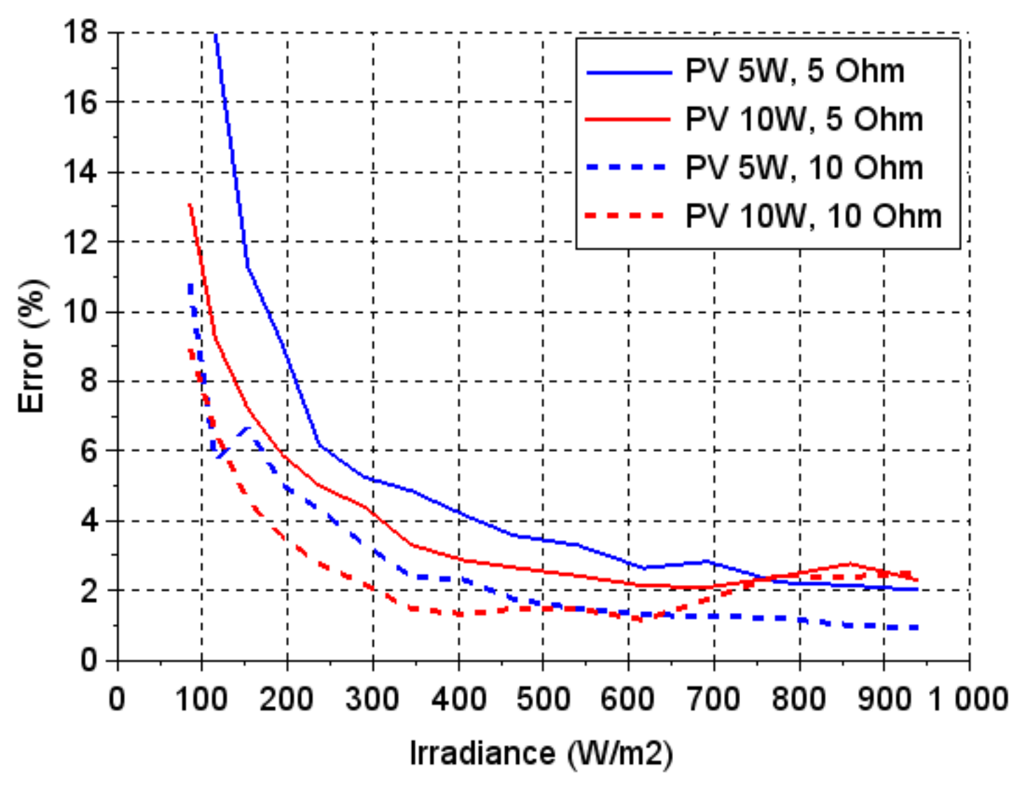
4. Results
5. Discussion
6. Conclusions
Author Contributions
Funding
Conflicts of Interest
Appendix A


| Name | Symbol | Value | Unit |
|---|---|---|---|
| Dimension | W × L | 290 × 330 | mm |
| Peak power | Pmax | 10 | W |
| Maximum power current | Imp | 0.57 | A |
| Maximum power voltage | Vmp | 17.49 | V |
| Short circuit current | Isc | 0.61 | A |
| Open circuit voltage | Voc | 21.67 | V |
| Name | Symbol | Value | Unit |
|---|---|---|---|
| Dimension | W × L | 231 × 186 | mm |
| Peak power | Pmax | 5 | W |
| Maximum power current | Imp | 0.30 | A |
| Maximum power voltage | Vmp | 16.5 | V |
| Short circuit current | Isc | 0.34 | A |
| Open circuit voltage | Voc | 21.0 | V |
Appendix B


Appendix C. Analysis of the Errors
- δm-i: error between the measurement results and the model of an ideal converter (Equation (1));
- δm-ni: error between the measurement results and the model of a non-ideal converter (Equation (3)).
| Irradiance W/m2 | 5 Ω Load Resistance | 10 Ω Load Resistance | ||
|---|---|---|---|---|
| δm-i % | δm-ni % | δm-i % | δm-ni % | |
| 85 | - | - | 19.8 | 10.8 |
| 115 | 33 | 17.9 | 15.2 | 5.71 |
| 153 | 27.5 | 11.3 | 16 | 6.69 |
| 193 | 25.7 | 9.08 | 14.5 | 5.04 |
| 237 | 23.3 | 6.16 | 13.8 | 4.32 |
| 289 | 22.5 | 5.25 | 12.9 | 3.33 |
| 345 | 22.1 | 4.85 | 12.1 | 2.4 |
| 406 | 21.5 | 4.17 | 12 | 2.31 |
| 465 | 21 | 3.57 | 11.4 | 1.75 |
| 540 | 20.8 | 3.3 | 11.2 | 1.47 |
| 617 | 20.2 | 2.64 | 11 | 1.30 |
| 692 | 20.3 | 2.82 | 10.9 | 1.26 |
| 776 | 19.8 | 2.23 | 10.8 | 1.20 |
| 860 | 19.7 | 2.14 | 10.6 | 0.995 |
| 940 | 19.6 | 2.01 | 10.5 | 0.908 |
| Irradiance W/m2 | 5 Ω Load Resistance | 10 Ω Load Resistance | ||
|---|---|---|---|---|
| δm-i % | δm-ni % | δm-i % | δm-ni % | |
| 85 | 29 | 13.1 | 18 | 8.95 |
| 115 | 25.8 | 9.22 | 15.9 | 6.56 |
| 153 | 24.1 | 7.22 | 14 | 4.57 |
| 193 | 23 | 5.89 | 13.1 | 3.56 |
| 237 | 22.2 | 5 | 12.3 | 2.76 |
| 289 | 21.7 | 4.41 | 11.8 | 2.19 |
| 345 | 20.7 | 3.31 | 11.1 | 1.46 |
| 406 | 20.3 | 2.86 | 10.9 | 1.32 |
| 465 | 20.1 | 2.66 | 11 | 1.48 |
| 540 | 19.9 | 2.42 | 11 | 1.47 |
| 617 | 19.6 | 2.13 | 10.7 | 1.15 |
| 692 | 19.5 | 2.08 | 11.2 | 1.74 |
| 776 | 19.7 | 2.39 | 11.8 | 2.42 |
| 860 | 20 | 2.76 | 11.7 | 2.38 |
| 940 | 19.5 | 2.29 | 11.8 | 2.52 |
Appendix D

References
- Rosu-Hamzescu, M.; Oprea, S. Practical Guide to Implementing Solar Panel MPPT Algorithms, Application Note AN1521; Microchip Technology Inc.: Chandler, AZ, USA, 2013; pp. 1–13. [Google Scholar]
- Koutroulis, E.; Kalaitzakis, K.; Voulgaris, N. Development of a microcontroller-based, photovoltaic maximum power point tracking control system. IEEE Trans. Power Electron. 2001, 16, 46–54. [Google Scholar] [CrossRef] [Green Version]
- Bounechba, H.; Bouzid, A.; Snani, H.; Lashab, A. Real time simulation of MPPT algorithms for PV energy system. Int. J. Electr. Power Energy Syst. 2016, 83, 67–78. [Google Scholar] [CrossRef] [Green Version]
- Yilmaz, U.; Turksoy, O.; Teke, A. Improved MPPT method to increase accuracy and speed in photovoltaic systems under variable atmospheric conditions. Int. J. Electr. Power Energy Syst. 2019, 113, 634–651. [Google Scholar] [CrossRef]
- Enrique, J.; Durán, E.; Sidrach-De-Cardona, M.; Andújar-Márquez, J.M. Theoretical assessment of the maximum power point tracking efficiency of photovoltaic facilities with different converter topologies. Sol. Energy 2007, 81, 31–38. [Google Scholar] [CrossRef]
- Dolara, A.; Faranda, R.; Leva, S. Energy Comparison of Seven MPPT Techniques for PV Systems. J. Electromagn. Anal. Appl. 2009, 1, 152–162. [Google Scholar] [CrossRef] [Green Version]
- Ahmad, J.; Kim, H.-J. A Voltage Based Maximum Power Point Tracker for Low Power and Low Cost Photovoltaic Applications. Int. J. Electr. Energetic Electron. Commun. Eng. 2009, 3, 2350–2353. [Google Scholar]
- Zhang, L.; Hurley, W.G.; Wolfle, W. A new approach to achieve maximum power point tracking for PV system with a variable inductor. In Proceedings of the 2nd International Symposium on Power Electronics for Distributed Generation Systems, Hefei, China, 16–18 June 2010; pp. 948–952. [Google Scholar] [CrossRef]
- Jiang, J.A.; Huang, T.L.; Hsiao, Y.T.; Chen, C.H. Maximum Power Tracking for Photovoltaic Power Systems. Tamkang J. Sci. Eng. 2005, 8, 147–153. [Google Scholar]
- Banu, I.V.; Beniuga, R.; Istrate, M. Comparative analysis of the perturb-and-observe and incremental conductance MPPT methods. In Proceedings of the 8th International Symposium on Advanced Topics in Electrical Engineering (ATEE 2013), Bucharest, Romania, 23–25 May 2013; Institute of Electrical and Electronics Engineers (IEEE): Piscataway, NJ, USA, 2013; pp. 1–4. [Google Scholar]
- Houssamo, I.; Locment, F.; Sechilariu, M. Experimental analysis of impact of MPPT methods on energy efficiency for photovoltaic power systems. Int. J. Electr. Power Energy Syst. 2013, 46, 98–107. [Google Scholar] [CrossRef]
- Faranda, R.S.; Leva, S.; Maugeri, V. MPPT techniques for PV Systems: Energetic and cost comparison. In Proceedings of the 2008 IEEE Power and Energy Society General Meeting—Conversion and Delivery of Electrical Energy in the 21st Century, Pittsburgh, PA, USA, 20–24 July 2008; Institute of Electrical and Electronics Engineers (IEEE): Piscataway, NJ, USA, 2008; pp. 1–6. [Google Scholar]
- Azab, M. A New Maximum Power Point Tracking for Photovoltaic Systems. World Acad. Sci. Int. J. Electr. Electron. Eng. 2009, 3, 702–705. [Google Scholar]
- Freeman, D. Introduction to Photovoltaic Systems Maximum Power Point Tracking, Application Report SLVA446; Texas Instruments Incorporated: Dallas, TX, USA, 2010; pp. 1–7. [Google Scholar]
- Esram, T.; Chapman, P.L. Comparison of Photovoltaic Array Maximum Power Point Tracking Techniques. IEEE Trans. Energy Convers. 2007, 22, 439–449. [Google Scholar] [CrossRef] [Green Version]
- Abdi, B.; Mirtalaei, S.M.M.; Ghasemi, R. Reliability of MPPT Converter in Different Operating Modes. Int. J. Mach. Learn. Comput. 2013, 3, 274–278. [Google Scholar] [CrossRef] [Green Version]
- Test Report of MPPT & LED Driver PMP7647. Available online: https://www.ti.com/lit/ug/tidu220/tidu220.pdf?ts=1623939628814&ref_url=https%253A%252F%252Fwww.google.com%252F (accessed on 17 June 2021).
- Test Report of MPPT Charge Controller PMP7605; Texas Instruments. Available online: https://www.ti.com/lit/ug/tidu219/tidu219.pdf?ts=1623872781719&ref_url=https%253A%252F%252Fwww.ti.com%252Ftool%252FTIDA-00120 (accessed on 17 June 2021).
- Janke, W.; Walczak, M. Influence of output conductance on characteristic frequencies of switch mode BUCK and BOOST converter. Arch. Electr. Eng. 2017, 66, 165–178. [Google Scholar] [CrossRef] [Green Version]
- Janke, W.; Baczek, M.; Kraśniewski, J.; Walczak, M. Large-signal input characteristics of selected DC-DC switching converters Part I. Continuous conduction mode. Arch. Electr. Eng. 2020, 69, 739–750. [Google Scholar]


Publisher’s Note: MDPI stays neutral with regard to jurisdictional claims in published maps and institutional affiliations. |
© 2021 by the authors. Licensee MDPI, Basel, Switzerland. This article is an open access article distributed under the terms and conditions of the Creative Commons Attribution (CC BY) license (https://creativecommons.org/licenses/by/4.0/).
Share and Cite
Walczak, M.; Bychto, L. Influence of Parasitic Resistances on the Input Resistance of Buck and Boost Converters in Maximum Power Point Tracking (MPPT) Systems. Electronics 2021, 10, 1464. https://doi.org/10.3390/electronics10121464
Walczak M, Bychto L. Influence of Parasitic Resistances on the Input Resistance of Buck and Boost Converters in Maximum Power Point Tracking (MPPT) Systems. Electronics. 2021; 10(12):1464. https://doi.org/10.3390/electronics10121464
Chicago/Turabian StyleWalczak, Marcin, and Leszek Bychto. 2021. "Influence of Parasitic Resistances on the Input Resistance of Buck and Boost Converters in Maximum Power Point Tracking (MPPT) Systems" Electronics 10, no. 12: 1464. https://doi.org/10.3390/electronics10121464
APA StyleWalczak, M., & Bychto, L. (2021). Influence of Parasitic Resistances on the Input Resistance of Buck and Boost Converters in Maximum Power Point Tracking (MPPT) Systems. Electronics, 10(12), 1464. https://doi.org/10.3390/electronics10121464