Review

Low Melting Temperature Sn-Bi Solder: Effect of Alloying and Nanoparticle Addition on the Microstructural, Thermal, Interfacial Bonding, and Mechanical Characteristics

Department of Materials Science and Engineering, University of Seoul, 163, Seoulsiripdae-ro, Dongdaemun-gu, Seoul 02504, Korea
*
Author to whom correspondence should be addressed.
Metals 2021, 11(2), 364; https://doi.org/10.3390/met11020364
Submission received: 20 January 2021 / Revised: 8 February 2021 / Accepted: 17 February 2021 / Published: 22 February 2021

Abstract

:
Sn-based lead-free solders such as Sn-Ag-Cu, Sn-Cu, and Sn-Bi have been used extensively for a long time in the electronic packaging field. Recently, low-temperature Sn-Bi solder alloys attract much attention from industries for flexible printed circuit board (FPCB) applications. Low melting temperatures of Sn-Bi solders avoid warpage wherein printed circuit board and electronic parts deform or deviate from the initial state due to their thermal mismatch during soldering. However, the addition of alloying elements and nanoparticles Sn-Bi solders improves the melting temperature, wettability, microstructure, and mechanical properties. Improving the brittleness of the eutectic Sn-58wt%Bi solder alloy by grain refinement of the Bi-phase becomes a hot topic. In this paper, literature studies about melting temperature, microstructure, inter-metallic thickness, and mechanical properties of Sn-Bi solder alloys upon alloying and nanoparticle addition are reviewed.

1. Introduction

In recent years, lead-free solders having high reliable metallurgical, mechanical, and electrical properties have been widely applied not only to consumer appliances but also in industrial electronic products and automobile electronic products [1,2]. Electronic packaging trends move to miniaturization, high-density packaging, and high performance. Fast data communication is required in 5G and IoT (Internet of Things) fields, which need the development of a system in the package (SiP), package on a package (PoP), Wafer level packaging (WLP), 2.5D &3D semiconductor package, system on chip (SOC), and System Integration package (SIP) as packaging technologies [3]. Various lead-free solders have been proposed after the restriction of hazardous substances (RoHs) in the electronic industry. Typical lead-free solders include series of Sn-Ag (Sn-3.5wt%Ag) (all the compositions are in weight percent unless stated otherwise), melting point 221 °C), Sn-Cu (Sn-0.7%Cu, melting point 227 °C), Sn-Bi (Sn-58%Bi, melting point 139 °C), Sn-In (Sn-52%In, melting point 118 °C), Sn-Ni (Sn-0.1%Ni, melting point 231 °C), Sn-Zn (Sn-9%Zn, melting point 198 °C), Sn-Ag-Cu (Sn-3%Ag-0.5%Cu, melting point 217 °C) [4,5,6,7,8,9,10,11,12,13]. The difference in thermal expansion between the Si chip and the substrate increases due to the modularization and enlargement of electronic components. The higher the soldering temperature, the more thermal deformation of electronics components, and, resultantly, defects appear frequently. In addition, in moisture sensitive packaging, defects such as delamination or pop-corning failure can be accentuated at a higher temperature [14]. To solve these problems, there is an increasing need for research on low melting point solders, such as Sn-Bi or Sn-In alloys [15]. Sn-Bi solder is cost effective as compared to Sn-In and has better thermal reliability due to its relatively higher melting temperature. The low melting point solder is suitable for temperature-sensitive fabrics [16] and flexible substrates [17]. For example, Sn-Bi solder can be used for the bonding of electronic devices on a wearable or flexible substrate, like a fabric, as shown in Figure 1 for smart fabrics [16]. However, Sn-Bi eutectic solder has some drawbacks like low ductility and poor fatigue properties [18].
To overcome the problems mentioned above, many studies have been performed, such as grain refinement by the addition of various alloying elements like Ag, Cu, Ni, In, Al, Sb, and so on [19,20,21,22]. Addition of nanoparticles or fibers like CNT, Y2O3, Al2O3, ZrO2, TiO2, Cu, and Ni to solders is another approach [23,24,25,26,27,28]. The epoxy-containing solders, which form an epoxy layer over the solder fillet, is also helpful to enhance shear strength and drop reliability [29,30,31,32,33]. Therefore, in this paper, we would like to introduce the significant results corresponding to the melting temperature, spreading and wetting, microstructure, inter-metallic thickness, and mechanical properties of Sn-Bi solder upon alloying and nanoparticle addition. A special focus has been given to Sn-58Bi composition due to their low melting temperature and their eutectic microstructure.

2. Melting Temperature and Wetting Property of Sn-Bi Solders

2.1. Effect of Alloying Addition on the Melting Temperature of Sn-Bi Solder

The Sn-Bi-based alloys, which is a low melting point solder that is increasingly applied to suppress thermal deformation of electronic parts and to low temperature process in multi-reflow, should have a low melting point and reliable properties. Among the low-temperature solders of Sn-Bi and Sn-In based, Sn-58%Bi is a representative solder with low cost, good solderability, and environmentally-friendly characteristics. Sn-Bi-(0.2–0.5)%Ag solders are also popular for a low-temperature application, which has high ductility, good wettability, a suitable mechanical property, and a low melting point [34,35,36,37].
Sn-Bi-based solders have a range of melting temperatures based on alloying elements. Therefore, a detailed and intensive study is required to find suitable applications. Table 1 shows the effects of various additive elements such as Ti, Cu, Ag, In, Sb, Co, Zn, and Rare earth (RE: Ce & La) on the melting point of Sn-58%Bi eutectic solder. Sn-Bi eutectic composition is known as Sn-56.97%Bi and its melting point as 138.8 °C by NIST (National Institute of Standards and Technology), and Sn-57%Bi and 139 °C in the phase diagram by the ASM International. However, in many publications, Sn-58%Bi with a melting point of 138–139 °C is also used as the eutectic composition [19,38,39]. Anyway, this eutectic melting point may have slight variations depending on the heating rate of Sn-58% alloy. As shown in Table 1, it is reported that Sn-58%Bi has a melting range of 130.2 °C (solidus temperature)–139 °C (liquidus temperature) or higher such as 139.5–147.6 °C, 139.4–148.0 °C [19,21]. On the other hand, according to Zhou et al. [22], when the Bi content in Sn-Bi is lowered to Sn-35%Bi, the solidus temperature remains at 138 °C, but the liquidus temperature rises to 186 °C. Additionally, Sn-58%Bi shows 139.06 °C to 143.11 °C, but when 0.5% and 1 wt% of Ti is added, it exhibits small changes like 138.98 °C to 142.70 °C and 139.18 °C to 143.49 °C, respectively [22]. By adding 0.5%Ag to Sn-58%Bi, the melting point is reduced to ~1 °C, and it is known to have a melting range of 135.7 °C (solidus) to 138.2 °C (liquidus) [39]. This can be attributed to the formation of Ag3Sn inter-metallic compounds (IMC) in the Sn-rich phase as explained in literatures [40,41,42,43,44,45]. At 0.5% of Ag addition, the composition might be close to the eutectic composition in the Sn-rich (Sn+Ag3Sn+Bi) phase. By the addition of 1% Ag to Sn-58Bi, it has a melting point of 137–142 °C [46] and with the addition of 2%Ag, 139.1–145.4 °C [47], and the melting point of Sn58 wt%Bi+4%Ag increases to 138.1–145.5 °C [48]. Indium is usually added as a melting point depressant and a ductility improving the element in Sn-58wt% Bi eutectic solder. The ductility enhancement is due to the formation of Bi-In inter-metallic phases. However, the high cost of indium is a drawback. With the addition of 3% In to Sn-58Bi, the melting range is 119.9 °C (solidus)–140.5 °C (liquidus) (peak temperature, 133.7 °C) [48]. Sn-58Bi-1Ag-1In has a melting point of 133 °C (solidus)–137 °C (liquidus) [46], and Sn-58Bi-3In-4Ag is 116.9 °C–138.1 °C (peak temperature, 134.1 °C) [48]. If 0.5 wt% Ti is added to Sn-58Bi solder, the melting point becomes 138.98–142.70 °C [22], and the addition of 0.5%Co to Sn-58Bi, where melting temperature is increased to 140.1–145.0 °C [49].
On the other hand, when Sb is added to Sn, the melting point increases. The melting temperature of peritectic composition (Sn-6.2 wt%Sb) is 243 °C, which is about 11 °C higher than that of Sn, 232 °C. Sn-53.2%Bi-5.8%Sb has a melting range of 139.5–149.2 °C [21]. According to Zhang et al. [43], when the Bi content is reduced from 52% to 44% at a constant Sb of 1.8 wt%, the melting range becomes large from 11.4 °C to 38.6 °C. The melting range of Sn-44%Bi-1.8%Sb is 141.9–180.5 °C. Thus, when Sb is added to Sn-Bi solder and Bi content decreases, then the melting point of Sn-Bi-Sb increases. However, it is difficult to say that this is the effect of pure Sb because the Bi content is also reduced. When Sb is added from 1% to 2.8 wt.% in Sn-48 wt%Bi solder, solidus temperature increase from 140.6 °C to 143.6 °C, but liquidus is a little affected. Dirasutisna et al. [50] reported the melting point value of Sn-52%Bi at 142.28 °C as a eutectic point. In addition, the melting point of Sn-52% Bi-Al increased with increasing Al content such as 144.38 °C for Sn-52%Bi-0.05%Al and 144.6 °C for Sn-52%Bi-0.25%Al. The melting point of S-52%Bi-x%Al is slightly higher than Sn-30%Bi and Sn-70%Bi. However, the authors did not mention whether the values correspond to a liquidus temperature [50]. The addition of rare earth (RE) (0.1 wt% Ce and La) has a trivial influence on the melting temperature of Sn-58% Bi-Al alloy, and the melting point of Sn-58 Bi remains unaffected with the co-addition of Ag and In [39]. With the addition of 0.1% of Cu to Sn-40%Bi, the endothermic peak decreased to 132.2 °C compared to 139 °C of Sn-58%Bi. On the other hand, the addition of 2% Zn (Sn-40%Bi-2%Zn-0.1%Cu) increases the peak to 136.3 °C [19].
Meanwhile, Xu et al. [45] reported on the melting point and spreading properties of Sn-(8–50%) Bi-(0.5–5%) Cu solder. In Sn-50%Bi-(1–5%) Cu, with increasing Cu content from 1% to 5%, the differential scanning calorimetry (DSC) peak point raises from 154 °C to 157 °C. However, in Sn-10%Bi-(0.5–3%) Cu, the addition of Cu did not affect the DSC peak point. Hence, the effect of Cu on the melting temperature of Sn-Bi solder is trivial.

2.2. Effect of Nanoparticles Addition on Melting Temperature of Sn-Bi Solder

The addition of nanoparticles has no significant influence on the melting temperature of the SnBi solder. Liu et al. [41] reported the melting point of Sn-58%Bi (SB), SB-0.5%Y2O3, SB-1%Y2O3, SB-3%Y2O3 as 138.77 °C, 139.15 °C, 138.83 °C, and 139.2 °C, respectively. By the addition of 3%Y2O3, only 0.43 °C of the melting point is increased. This is because the oxides are stable and non-active in the solder melting state and their contents are small [51]. Similarly, Ti nanoparticles did not significantly affect the melting temperature of Sn58Bi solder [42].

2.3. Effect of Alloying Elements on Wetting and Spreading of Sn-Bi Solder

The solder should have excellent spreading and wetting properties on the metal surface of the electronic parts to be joined, which is a basic requirement for suppressing defects during soldering and securing performance and workability. The wettability of a molten solder can be affected by the surface tension of the solder, metal substrate, temperature, atmosphere, and flux. If other factors are fixed except surface tension, the alloying element to the solder, which can change surface tension, is a very influential factor on the wettability. The driving force for the wetting is surface energies between liquid solder and solid substrate represented by Young’s Equation (1) and their interfacial reaction [52].
Cos θ = γ SV γ SL γ LV
where γ SV is the solid-vapour surface tension, γ SL is the solid-liquid interface surface tension, and γ L V is the liquid-vapour surface tension. For a good wetting and spreading Cosθ and γ SV should be maximum and γ LV is minimum. Dong et al. [39] reported that, when 0.1% RE (Ce and La) added to the Sn-58%Bi, it enhanced the wettability on a Cu substrate.The 0.5% Ag addition to Sn-58%Bi can improve the wettability of the SnBi solders [51]. Meanwhile, Sebo et al. [52] reported through the sessile drop method that the wetting angle in the air with flux increased slightly as the Ag content in the solder increased. However, wetting on the Cu substrate in N2+10%H2 gas, oppositely, shows the wetting angle slightly decreased as the silver content in the solder increased. In Sn-10at%-Bi-(3.3–10) at%Ag series solder, the wetting angle can be reduced with increasing Ag content under N2+10H2 atmosphere [52]. When Cu is added into Sn-Bi-Cu solder, then Cu concentrates on the interface and causes a wetting angle reduction [53]. Sn-Bi-Cu solders are reported to have better thermal resistance and reliability [54]. According to Xu et al., the spreading area of Sn-Bi-Cu solder increased due to a lower melting temperature [55]. The optimum content showing the maximum spreading area is reported as Sn-17%Bi-0.5%Cu [55]. Zang et al. [36] studied 69.5 wt%Sn-30 wt%Bi-0.5 wt%Cu on Cu substrate obtained at 220 °C, 275 °C, and 350 °C. The higher the temperature is, the better the wettability becomes. 69.5 wt%Sn-30 wt%Bi-0.5 wt%Cu at 220 °C has a better wettability on Cu substrate than Sn-3.5%Ag-4.8%Bi and Sn-3.8%Ag-0.7%Cu [56].
According to Wang et al. [57], Sn-38%Bi-1.5%Sb-0.7% Ag solder has a shorter wetting starting time (zero-cross time, t0) than Sn-58% Bi in 160–200 °C range for water-based flux, but not much difference for halide-free alcohol-based flux. However, the wetting force of Sn-38%Bi-1.5%Sb-0.7%Ag solder, 0.6 mN or more, is a little higher than that of Sn-58%Bi, 0.6 mN or less, whereas the soldering temperature and flux do not have a significant effect on the force. Meanwhile, t0 is greatly influenced by the flux type and between alcohol-based flux and a water-based one. The former has a shorter t0, less than half the value of the latter, for both of Sn-38%Bi-1.5%Sb-0.7%Ag and Sn-58%Bi.
Various studies about solder wetting properties and their analysis are reported by the authors, such as withdrawal force of wetting curve to calculate liquid solder surface tension (γLF) and contact angle (θC) between the wetting coupon derived as Equations (2) and (3) [58,59].
γ LF = ρ g 4 [ 4 F 2 ( ρ gPH ) 2 + H 2 ]
θ C = Sin 1 [ 4 F 2 ( ρ gPH 2 ) 2 4 F 2 + ( ρ gPH 2 ) 2 ]
where F is measured by the wetting force, P is the perimeter of the specimen, H is the meniscus height, ρ is the density of the solder, and g is the gravity acceleration constant. The author [60] also studied wetting property in the solidification interval to evaluate the soldering feasibility below the liquidus temperature. The solidification interval is recommended to be <10 °C to achieve a defectless bonding interface. Larger solidification intervals lead to hot tearing during solidification at the solder joints. The Sn-3%Cu, Sn-7%Ag, and Sn-(10–60)% Pb showed good wettability even lower than liquidus temperature, but the wettability of low-temperature solder, Sn-65%Bi and Sn-40%In, is poor. Wetting properties of solder under fluxless state were reported previously by the author for the basic study of fluxless soldering [61,62,63]. Sn-57%Bi having 53.0° wetting angle at 190 °C without flux showed better wettability on the Au/Cu/Cr-coated glass substrate compared to Sn-3.5%Ag of 67.2° at 270 °C, Sn-5%Sb of 60.1° at 290 °C, Sn-37%Pb of 69.4° at 230 °C and non-wetted Sn-51% In solders. Generally, to achieve good solderability, the following conditions must be satisfied. (a) The molten solder wets the surface of the base metal where the recommendable zero-cross time is less than 1.0 s, and solder spreads out well with a contact angle less than 60° on a substrate. (b) A capillary phenomenon in which molten solder is sucked in the gap between two base metals, which is the recommendable gap in this case, is less than 0.3 mm. (c) The diffusion, which is the interatomic transfer between the solder and the base metal surface, must occur quickly [64]. In Sn-Bi-Sb solder, if Sb is added lower than 2 wt%, then the wettability of Sn-48%Bi will be improved [43]. Meanwhile, the addition of In lower than 4% also enhances the wettability of Sn-(53–58)%Bi solder [18]. In addition, the spreading ratio of Sn-(53–58)% Bi solder decreased from 73% to 65% for 190 °C, from 70% to 63% for 170 °C with increasing In content up to 4% In element was confirmed to participate in the interfacial reactions forming Cu-Sn-In IMCs and affect the wettability of Sn-Bi solder on Cu substrates [16]. The addition of Bi up to 20% to Sn-3.5%Ag and Sn-8.2%Zn solders reduces the wetting time (zero-cross time) and wetting activation energy [65]. Sn-38%Bi-1.5%Sb-0.7Ag solder has better wettability in terms of the wetting time, namely shorter zero-cross time, than that of Sn-58%Bi solder. However, the maximum wetting force of both solder alloy is not very different [57].

2.4. Effect of Nanoparticle Addition on Wetting and Spreading Property of Sn-Bi Solder

Nanoparticles are also found to influence the wetting and spreading characteristics of SnBi solder. The addition of 2.5% Mo nanoparticle to Sn-Bi increases the wettability of the solder [66]. Sn-Bi solder with the Ni nanoparticle has a lower contact angle than that of Sn-Bi [67,68]. According to Liu et al [69], the wetting properties of the Sn-58Bi solders are significantly improved by the addition of Y2O3 up to 1%, which means the spreading area heated at 175 °C increased approximately from 30 mm2 to 36 mm2. However, it decreased when 3 wt%Y2O3 is included. Too much nanoparticle content decreases spreadability because nanoparticles embedded into solder matrices inhibit the flow of molten solders by increasing its viscosity, which ‘pins’ the leading edge of the molten solder from further spreading. Thus, it can be said an abundance of nanoparticles in composite solders reduces the wettability of solder alloys. The addition of SnO2 nanoparticles up to an optimal amount was beneficial for spreading and wetting properties as well, as an increase in nanoparticle addition decreases the zero cross time and increases the spreading ratio. Figure 2 shows the spreading area for the RE alloying and Ti nanoparticles. It can be seen that the addition of 0.1% of Ti nanoparticles decreases the spreading area whereas a similar addition level of RE (Ce and La) increases the spreading area. Thus, the favorability of additives for the wetting depends on the additive element and the addition level [70]. Yim et al. [71] reported a conductive adhesive bearing Sn-58%Bi solder powder with 0.03% MWCNT (Multi-walled carbon nanotube). Sn-58%Bi with MWCNT resulted in good wettability and solder fillet shape, but too much addition like 2% MWCNT gave a defect in the solder joint.

3. Microstructure and IMC

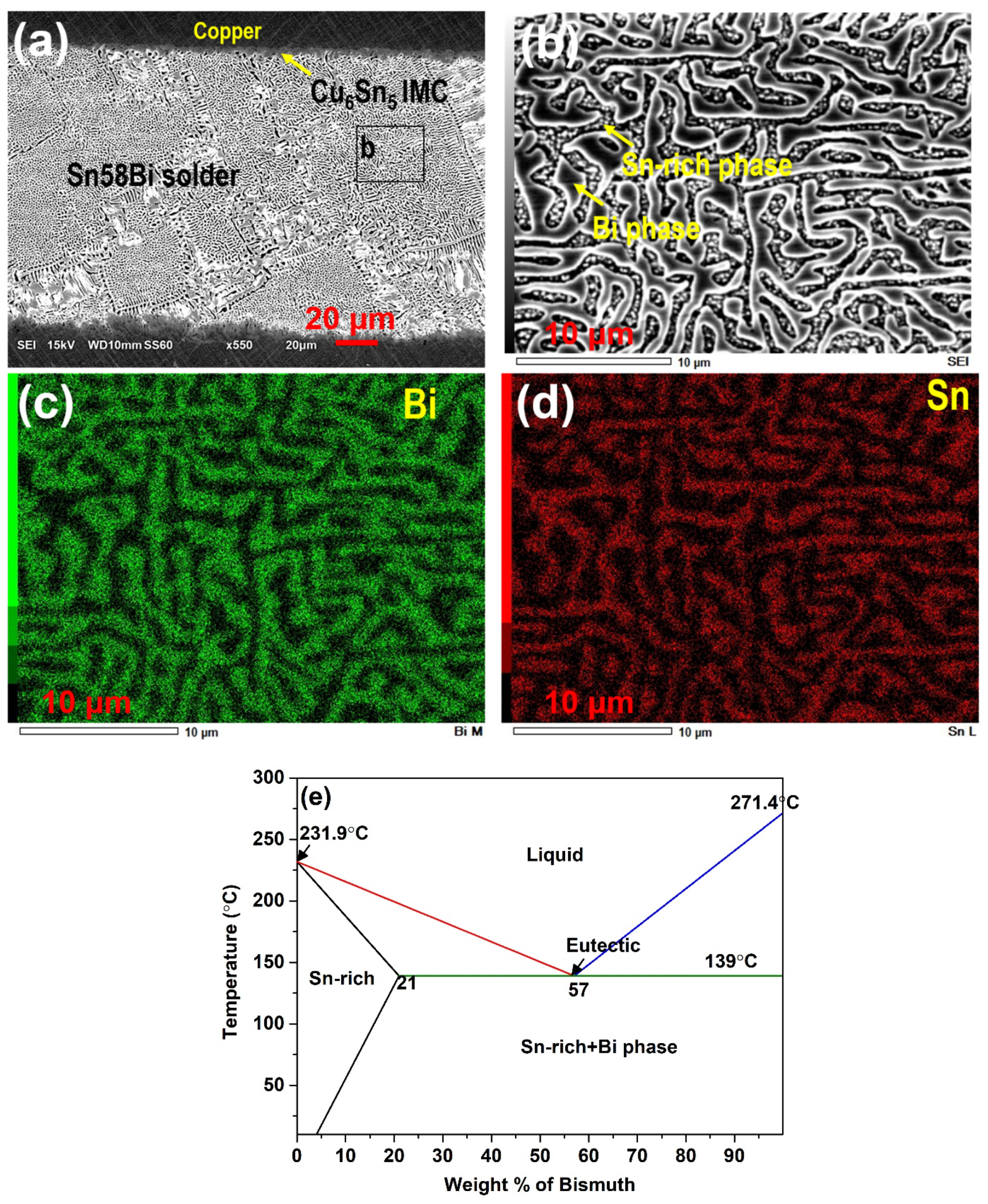
3.1. Effect of Alloying on the Sn-Bi Microstructure

Generally, the microstructure of Sn-58%Bi eutectic solder shows a lamellar mixture of a ductile β-Sn phase and a brittle Bi phase. Bi-rich phase is almost pure and Sn solubility in Bi is around 0.11 wt% at eutectic temperature, and at 25 °C 0.6 wt% [70,72] Meanwhile, Bi solubility in Sn is 21% at 139 °C and decreased to 4.5 wt% at 50 °C, and around 3.2 wt% or 2.0 wt% at 25 °C [72,73,74]. In general, the two phases of the β-Sn (Sn-rich) phase and the Bi-rich phase show a typical lamellar structure. However, at high cooling rates, regions discontinuous eutectic regions of random orientation appear in addition to the typical lamellar structure [75]. Figure 3a–d shows a SEM microstructure and elemental analysis of Sn-58Bi solder having lamellar eutectic Sn-rich and Bi phase. Figure 3e shows the Sn-Bi phase diagram. The alloying elements of solder have a lot of influence on the Sn-58%Bi microstructure. The microstructure of Sn-58%Bi-x% In alloys was investigated by Chen et al. [18]. The Sn-58%Bi solder microstructure was a typical lamellar eutectic structure that consists of alternated Bi and Sn phases. By adding In, the amount of spherical primary Sn-rich phase increases. Granulate Bi-In phases are formed by adding 4%In. The Bi-In particles were mainly distributed in the Sn matrix and along with the Bi phase [18].
According to Sakuyama et al. [76], by the addition of 0.5 wt%Ag, a small amount of Ag3Sn IMC was produced and >1 wt%Ag, which results in the growth of Ag3Sn and reduction of ductility. The coarsening rate of the Bi-rich phase in the Sn-58%Bi solder joint under thermal aging at 120 °C is reduced by the addition of 1 wt% Cu [40]. The addition of 0.5 wt% of Sb to Sn-58%Bi refines the grain size of solder, and addition of 1% Sb produces SnSb IMC dispersed in the Sn phase near the grain boundaries of the eutectic structure. This SnSb IMC suppresses the growth of the eutectic structure, which results in a finer grain size and higher elongation [41]. Addition of 0.5 wt% Cu to Sn-58%Bi, produces dispersed Cu6Sn5 IMC in the solder, but sometimes several tens of microns in size also reduces the grain size of Sn-58%Bi.
According to Mokhtari et al. [77], the thickness of the interfacial IMCs of the eutectic Sn-Bi solder, thermally aged at 80 °C up to 1008 h, is considerably greater than that of the 0.5 wt%In and 0.5 wt%Ni-bearing solder joints. Sn-58%Bi solder with 0.5 wt%Ni addition shows Ni3Sn4 IMC in the eutectic structure, and it shows a regular eutectic area in the form of partly fishbone. Even Ni is added. The size of the Bi phase is slightly reduced compared to Sn-58%Bi. The Sn-58%Bi and 0.5%Ni-bearing solder show coarsened brittle Bi-rich phases, while there is no sign of Bi-phase coarsening in the 0.5%In-bearing solder. Addition of 0.5 wt% Zn to Sn-58%, where Zn exists as a needle-like shape, increases the grain size slightly compared to Sn-58%Bi. Zhou et al. [78] reported that both 0.5 wt% and 1 wt% Zn effectively refined the eutectic Sn-58%Bi alloy microstructure. This exhibits promising microstructural results and has a fractured path within the solder bulk [78,79,80]. In Sn-58Bi-0.5%Ti and Sn-58Bi-1%Ti solders, the matrix showed the irregular and regular eutectics, and the Sn-rich phase was easily observed, and microstructure, especially the Bi-rich phase, was refined. Mostly, smaller Ti6Sn5 IMCs were uniformly distributed in the Sn-58%Bi matrix [75]. Therefore, it can be said that grains are refined by adding 1 wt% of Ti, 0.5 wt% of Ag, Sb, In, Ni, or 0.5–1 wt% of Cu to Sn-58%Bi solder. Meanwhile, 0.5 wt% Zn addition can cause the growth of the grains of Sn-58%Bi solder. It is found that Cu reacts only with Sn in the Sn-Bi-Ag/Cu solder system, not with Ag or Bi [79]. Cu-Sn reaction is highly predomimant because of higher availability of Cu from the Cu substrate [80]. Because of the formation of the Cu6Sn5 IMC, Ag and Bi are expelled from the IMC reaction into the molten solder between the IMC scallops [52].

3.2. Nanoparticles Effect on Sn-Bi Microstructure

Various types of nanomaterials, such as nanometal (Ni, Cu, etc.), nano-ceramic (Al2O3, SiC, etc.), or nano IMC (Cu6Sn5, etc.) powders are added to Sn-58%Bi solder. When the appropriate amount of nanoparticles is added, the solder grains become finer [27,67]. Nano-sized particles added to the solder act as nucleation sites in the matrix during the solidification of the solder. This makes the phase of the solder structure refined by acting as an inoculant to generate a lot of solid nuclei during solder solidification. In addition, the pinning of grain or IMC can also suppress its growth. According to Y. Lin et al. [81], addition of Ag nanoparticles to the Sn-58% Bi refined the solder matrix microstructure, suppressed the interfacial IMC growth. The improvement was different from the Ag particle size. The addition of 76-nm Ag nanoparticles generated the best improvement: refining the microstructure by 49.1% and reducing the Cu-Sn IMC growth exponent from 0.394 to 0.339, suppressing the IMC thickness by 39.7% after 180 min at 220 °C. The improvements obtained from both of larger (133 nm) and smaller (31 nm) Ag nanoparticles were much more imperceptible than those for 76-nm Ag nanoparticles. Figure 4 shows the interphase values upon nanoparticle addition. As can be seen, the interphase spacing is lower for the graphene, Cu, and Ni nanoparticles addition. The improvement mechanisms were explained by refinement.
Nano-particles in the solder is known to be absorbed to the surfaces of IMCs in the bulk or in the bonding interface and suppress the growth of the IMCs. The number of absorbed nano-particles on the IMC (changed grain > IMC) surface can be derived as Equation (4) [81].
N K = C RT d γ K dC
where, N K ; amount of absorbed nano-particles per unit area, C, total amount of nano particles, RT, thermal energy per mol, γ K , and surface energy of IMC surface without nano-particles per unit area.
By integration,
γ C K = γ 0 K RT 0 C N K C dC
where, γ K C , the surface energy per unit area of the IMC (original equation, ‘grain’) adsorbed with nanoparticles, γ K 0 , and the surface energy per unit area of the IMC (original equation, ‘grain’) not adsorbed with nanoparticles. Meanwhile, the total surface energy can be expressed by Equation (6) [81].
K γ 0 K A K = K ( γ 0 K RT 0 C N K C dC ) A K
This is a constant, and the value must be increased or minimized surface energy. In other words, the grain growth rate should be decreased for maximum adsorption amount. However, in the case of an alloy containing an excessive amount of nanoparticles in the solder, the effect of adding nanoparticles is reduced due to agglomeration between nanoparticles, so that the suppression effect of the intermetallic compound and the β-Sn region in the alloy base decreases. However, when optimal nanoparticles are added to the solder, the grain size of the β-Sn in the solder also decreases. The reason can be that uniformly dispersed nanoparticles act as nucleation inoculants, which can suppress the growth of Sn grain. Similarly, A. Gain et al. [67] found that the β-Sn region and Ag3Sn were refined in the solder reinforced with nanoparticles of 0.5% Ni to Sn-35Bi-1Ag solder. The main reason can be that the nano Ni particles react with Sn to form Sn-Ni IMCs, and these IMC particles act as solid nucleation sites during solidification to inhibit grain growth. In addition, it was said that the addition of metal nanoparticles reduced the degree of supercooling to inhibit IMC growth and refine the structure. L. Zhang et al. [79] added 1–5 wt%Sn-3.0Ag-0.5 Cu (SAC) nanoparticles into a eutectic Sn-58%Bi solder paste. The Sn-Ag-Cu (SAC) nanoparticles refined the grain structure of the Sn-Bi solder. The reason is attributed to the presence of nanoparticles impediment to dislocation movement and pinning of grain boundaries to suppress the grain growth [82,83,84,85,86,87,88,89,90].
L. Shen et al. also studied the effect of Cu and Ni nanoparticles of 0.5 wt% to 4 wt% on the Sn-58Bi, and it was confirmed that the size of the phase of the solder matrix was decreased. The nanoparticles with 0.5 wt% give a great reduction of interphase spacing [27]. He et al. [87] reported the refinement effect of CNTs on the Sn-58%Bi solder when 0.03 wt% CNTs was added to Sn-58%Bi, the number of dendrites in composite solder reduces significantly, and the solder microstructure becomes finer because the CNTs can hinder grain growth. According to Yang et al., [90] Ni-coated carbon nanotubes (Ni-CNTs) with 0, 0.05, 0.1 and 0.2 wt% were added to Sn-58%Bi solder. The nano-composite solders exhibit finer microstructures when compared to the monolithic Sn-58%Bi solder. The reason can be attributed to the Ni3Sn4 heterogeneous nucleation in the solder that prevents the growth of the reticular structure, and the dispersed CNTs can hinder grain growth. Li et al. [91] prepared composite solders of Sn-58%Bi with 0, 0.03, 0.05, and 0.1wt% Cu6Sn5 nanoparticles. Addition of Cu6Sn5 nanoparticles sized of 10 nm refines the microstructure of Sn-58%Bi solder, and solder with 0.05 wt% Cu6Sn5 nanoparticles exhibited the best performance. Due to the refinement of the matrix phases, the strength of the solder increases, according to the Hall-Petch Equation (7) [92].
Δ σ Hall Petch = k u ( d m ) 1 / 2
where, k u : Hall-Petch constant according to the material and d m : phase size of the solder matrix L. Shen et al. studied the effect of Cu and Ni nanoparticles on the Sn-58%Bi microstructure, where the Sn-58%Bi solder consists of Sn-rich and Bi-rich phases [27]. As the weight percentage of the nano-fillers increases, the size of interphase spacing (IPS) generally decreases. Sn-58%Bi has 2.62 µm of IPS, but the addition of 0.5–4% Cu gives 1.73–1.21 µm and the addition of 0.5–4% Ni shows 1.77–1.18 µm. From the above results, optimal addition of nanoparticles can refine grains of Sn-Bi solder. However, excessive addition can invalidate the added effect. This can be attributed to the agglomeration of nanoparticles reported in various studies [93,94,95,96,97,98,99]. Agglomeration of a nanoparticles in the solder causes serious impediment tot eh reliability [100,101,102,103,104,105,106,107,108,109,110,111,112]. A. El-Daly et al. [111] reported that the effect of the rotating magnetic field (RMF), which generates Lorentz forced flow during solidification, on the microstructure of Sn-20%Bi and Sn-20%Bi-0.4 Cu alloys. The RMF caused grain refinement, reduced the gravity-induced macro-segregation, eliminated surface pinholes and serious dendrite structure, increased the eutectic areas, and decreased the eutectic lamellar spacing.
Lee et al. [113] added 0.5-g SiC nanoparticles, sized 45–55 nm, per 1 L of SnBi plating solution to make Sn-58%Bi solder by electroplating. Microstructural coarsening was suppressed by SiC nanoparticle addition. The amount of added SiC was 0.5 g per 1 L of SnBi plating solution. The average size of the Sn-58%Bi eutectic lamellar structure decreased 1.97 µm to 1.32 µm as soldered at 170 °C decreased by 32.9%. After aging at 100 °C for 400 h, the average eutectic size decreased from 4.59 µm to 2.37 µm, as much as 48.4% by adding SiC nanoparticles. Such refinement of a eutectic microstructure might have been due to the increased heterogeneous nucleation sites and impeded the phase or grain boundary movement by SiC nanoparticles [114,115,116]. Nanoparticles of oxides like ZrO2, CeO2, and Al2O3 also reported to refine the solder microstructure [85,86,87,88].

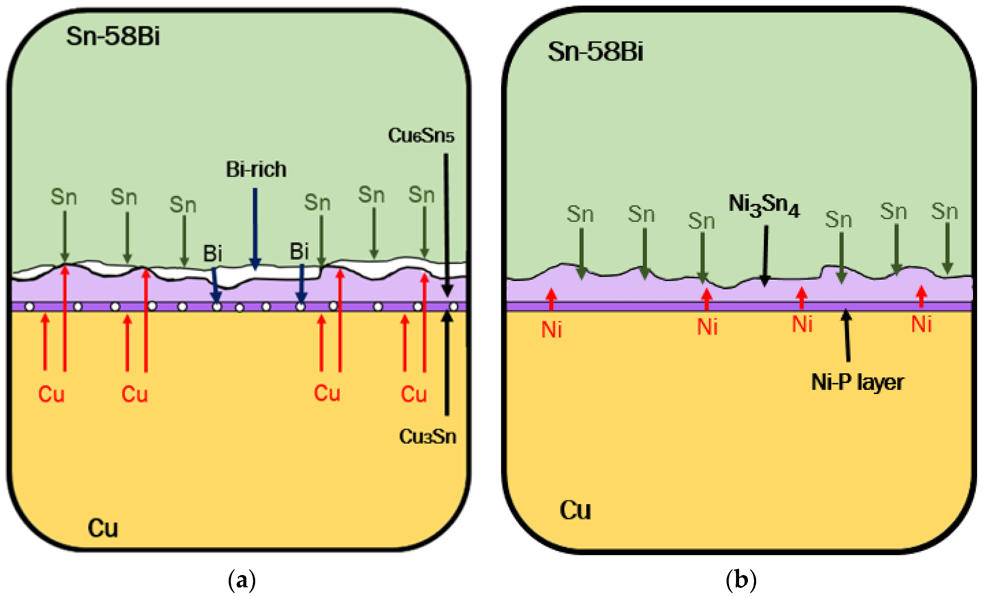
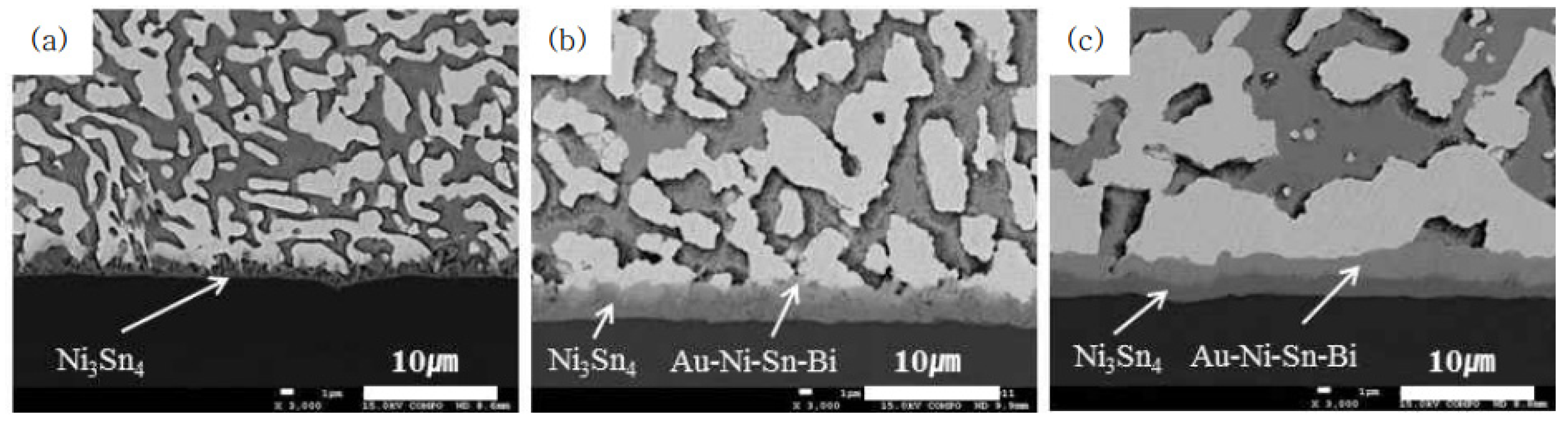
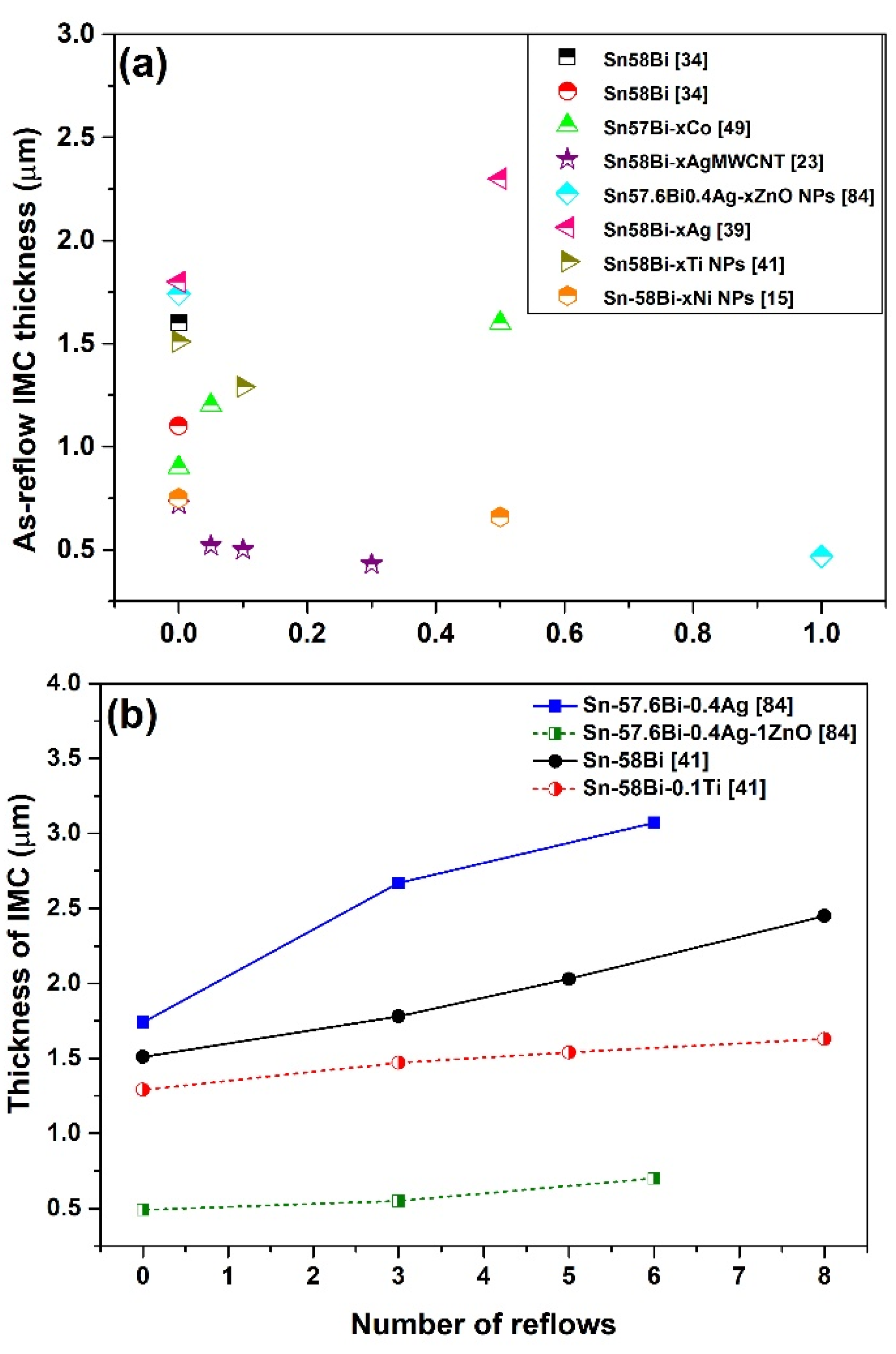
3.3. IMC at the Interface of Sn-Bi Solder

During soldering, molten SnBi solder penetrates into the gap between the metal electrode of the electronic component and the metal pad of the printed circuit board (PCB) by capillary flow and gets wetted on the metal surface. Then diffusion of atoms occurs between solder and metal parts of the electronic component and PCB by a concentration gradient [93]. Cu/Sn diffusion couples at 190–220 °C were also reported by Onishi et al., and they evaluated the inter-diffusion coefficients for the Cu6Sn5 and Cu3Sn IMCs [94]. The diffused atoms produce IMCs along the solder/Cu interface, and then bonding is completed as the molten solder solidifies [56]. The produced IMC along the bonding interface has a great influence on the mechanical strength and life of the soldered part. In the Sn-Bi solder/Cu substrate system, the interfacial IMC layer of η-phase (Cu6Sn5) produces at the solder side, and the IMC layer of ε-phase (Cu3Sn) formed at the Cu side. The IMCs increase with temperature and time. Between the molten Sn-Bi solder and Cu substrate, the Cu6Sn5 and Cu3Sn IMC grows parabolic from the beginning of the interfacial reaction at 250 °C [95]. The growth of the IMC layers consumes Sn atoms adjacent to the Cu6Sn5 layer, which leads to the formation of a Bi-rich phase layer along the Cu6Sn5 layer/solder interface after aging at 120 °C for 50 days [96,97]. At 120 °C, due to the 9 at%. solubility of Bi in Sn, Cu6(Bi, Sn)5 IMC grows at the interface. However, during the Cu6Sn5 to Cu3Sn transormation, the Bi phase is precipitated between Cu and Cu6Sn5. This is because Cu3Sn IMC has lower Bi solubility as compared to Cu6Sn5 IMC [97]. The crack propagated within IMC, between the Bi containing (Cu6(Sn, Bi)5) and Cu6Sn5 layer. The Bi-rich layer at the Cu3Sn/Cu interface of SnBi/Cu solder joints during the thermal aging process becomes a crack propagation path [10,88,98,99]. To suppress the Bi-rich layer, addition of Cu-X (Ag, Zn) to a substrate is useful. Furthermore, in Sn-58%Bi/Ni-P/Cu system, the Bi-containing layer was not observed since the Ni3Sn4 growth rate was slower. Figure 5 shows the schematic illustration of interfacial IMC formation in the Sn58Bi solder on Cu and Ni-P Coated Cu substrates.
By adding 0.5 wt% of In to Sn-58%Bi solder and reflowed at 170 °C, it is possible to suppress Bi coarsening and excessive Cu6Sn5 IMC formation at the interface between the solder and Cu substrate [77]. Sn-rich and Bi-rich phases show interlocked lamellar structures, and In was detected in the Sn phase. In atoms tend to replace the Sn atom and form Cu6(Sn, In)5 IMC. Conversely, when 0.5%Ni was added, Ni appeared to be included in the Bi-phase [109]. The addition of 0.5 wt% Ni to Sn-Bi solder can also give a similar IMC suppression. However, Ni atoms tend to replace the Cu atom and form (Cu, Ni)6Sn5 IMC with a lower growth constant [67,77].
The effect of Ni on the interfacial IMC of Sn-35%Bi-1%Ag between the Cu substrate is reportedly maintained at 200 °C for 30 min [67]. Ni suppressed IMC growth, namely, the thickness of the (Cu6Sn5+Cu3Sn) IMC layer of Sn-35%Bi-1%Ag-0.5%Ni and the Sn-35%Bi-1%Ag, which is about 3 µm and 4.8 µm, respectively. The growth rate of the IMC layer in the Sn-Bi-Ag on the Ni/Cu substrate decreased about 17.9% as compared to Sn-35%Bi-1%Ag/Cu system after a reaction at 200 °C for 5 min. In addition, the thickness of the IMC at the interface with Cu increased with increasing bonding temperature and the holding time at the bonding temperature. Meanwhile, according to F.Q. Hu et al. [100], various alloying elements have been added into the SnBi solder to suppress the IMC growth at the SnBi/Cu interface, and the elements can suppress the IMC growth only when they can form IMC with Cu, while the Ag addition cannot clearly slow down IMC formation [100,101,102]. By adding some alloying elements to the Cu substrate, the growth rate of IMC can usually be suppressed by decreasing the activity of Cu atoms [36,103,104].
Bi segregation around the SnBi/Cu interface after long-term aging can cause serious interfacial embrittlement [104,105]. However, according to F.Q. Hu et al. [100], the Ag element in the solder diffuses into the Cu substrate during the soldering and aging process for 21days and produces a Cu-Ag layer at the interface. Resultantly, the Bi segregation at the SnBiAg/Cu joint interface was suppressed, and the aging embrittlement at long-term aged SnBi/Cu will not occur. Shin et al. [106] studied the interfacial IMC between Sn-58%Bi solder paste and ENIG (5 µm of Ni-P, 0.15 µm of Au layer) finished Cu-pad PCB. Figure 6 shows the cross-sectional SEM micrographs of the solder joints between Sn-58%Bi solder and Electroless nickel immersion gold (ENIG) finished substrate after aging at 125 for 0, 30, and 100 h. The thickness of interfacial IMC is seen to increase with the aging time.
Similarly, Sn58Bi solder paste was reflowed at 170 ℃ to make a spherical shape bump on the ENIG and aged at 125 °C up to 1000 h. The IMC thickness grew to 3.3 µm after 500 h and about 4 µm after 1000 h isothermal aging treatment. IMC thickness growth at the interface is given by Equation (8) [117].
X = Dt + X 0
where X is the total IMC thickness, X0 is the initial IMC thickness, t is the time, and D is the diffusion coefficient of Cu and Sn atoms. Apart from Equation (7), Li et al. suggested that the mean thicknesses, x, of Cu6Sn5 can be described using the following equations [118].
x = K 1 3 t 1 3 , t < t 0
x = K 1 2 ( t t 0 ) + x 0 2 , t t 0
where t is the storage time, t0 and x0 are, respectively, the time and mean thickness at the transition point, and K1/3 and K1/2 are two growth rate constants. The growth rate constants are given by Equation (11) [118].
K = Aexp ( E a RT )
where A is a constant, Ea is the activation energy, R is the ideal gas constant, and T is the absolute temperature. Y. Kim et al. [117] reported the IMC morphologies at the interface of Sn-58% Bi paste/Cu pad reflowed at 190 °C, where the PCB surface treatments on the Cu pad were OSP (organic solder preservative), ENIG, and ENEPIG (Electroless Nickel Electroless Palladium Immersion Gold) of the substrate [117]. In the case of OSP, spherical micro-particles of Cu-Sn IMC (Cu6Sn5) were formed, and the size of spherical Cu6Sn5 particles, of several μm, did not change significantly even after 300-h and 1000-h aging. On the other hand, in the case of ENEPIG, coarse rod-shaped Ni3Sn4 IMC was formed at the initial stage of bonding, and after 300-h and 1000-h aging, changed to (Ni, Pd)3(Sn, Bi)4 IMC. The IMC size did not grow considerably, but fine irregularities appeared on the surface. In the case of ENIG, polygonal Ni3Sn4 IMC was formed in a soldered state and (Au, Ni) (Sn, Bi)4 IMC was slightly grown after 300 and 1000 h aging at 85 °C. Figure 7a shows the IMC thickness of Sn-Bi alloys with the addition of nanoparticles. According to Yang et al. [90], by the addition of Ni-coated CNT, the IMC layers in Sn-58%Bi/Cu and Sn-58%Bi-CNT/Cu interfaces changed from a scallop-type Cu6Sn5 to a thin layer (Cu, Ni)6Sn5. As the Ni-CNTs increase to 0.1 wt% and 0.2 wt%, the thickness of the IMC layer reduces. The transformation mechanism is explained to be the excrescent Ni-CNTs, which act as pin sites and restrain the diffusion of Sn atoms toward the interface [107]. Furthermore, IMC growth with multiple cycles proves to be beneficial for Ti [41] and ZnO [84] nanoparticles in addition to the Sn-Bi solder, as shown in Figure 7b.

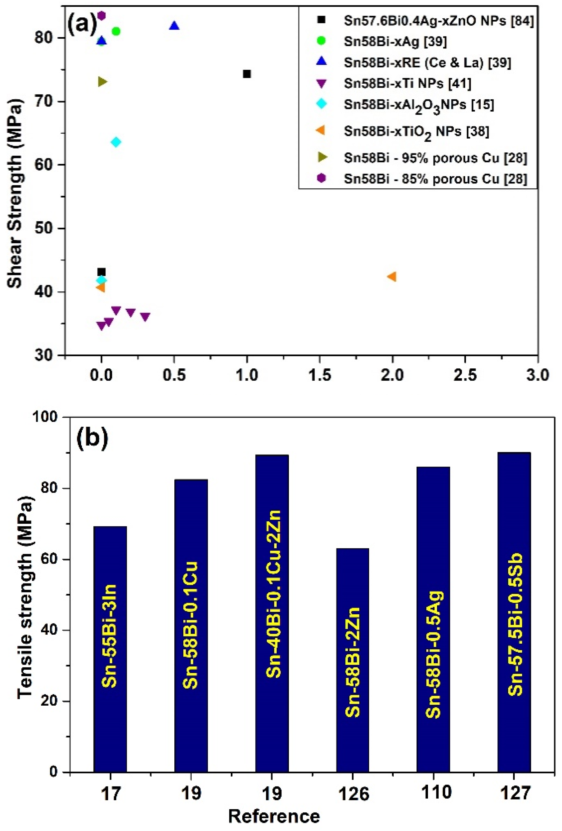
4. Mechanical Property of Sn-Bi Solder

According to Shimokawa et al. [108], Sn-57%Bi-1%Ag had higher tensile strength than that of Sn-37%Pb, close to 60 MPa for Sn-57%Bi-1Ag and around 35 MPa for Sn-37%Pb. However, in elongation Sn-37%Pb of slightly more than 40% is a little better than Sn-57%Bi-1%Ag having a little lower than 40%. Mokhtari et al. [77] reported that the addition of 0.5 wt% In or Ni to sn-58%Bi did not significantly affect the Young’s modulus. When 0.5 wt% Ni is added to Sn-58%Bi, the tensile strength slightly increases, but both of Sn-58%Bi and Sn-58%Bi-0.5% Ni have higher tensile strength than 50 MPa, and the difference is not large. However, Sn-58%Bi-0.5%In having around 45 MPa showed lower tensile strength than that of Sn-58%Bi. In terms of elongation, Sn-58%Bi-0.5%In showed the highest value of around 65%, and was followed by Sn-58%Bi around 35% and Sn-58Bi-0.5%Ni approximately 15%. When 0.5 wt% Ni was added, the Sn-58%Bi elongation decreased drastically due to the formation of Ni3Sn4 IMC in the solder. On the other hand, when 0.5 wt% In was added, the ductile fracture surface with dimples were observed. Chen et al. [17] reported that tensile strength changed slightly with increases in addition to Sn-(53–58)%Bi, which means tensile strength decreased from approximately 72 MPa to 68 MPa up to 3% In, and increased to 69 MPa at 5% In. Meanwhile the elongation increased remarkably from 20% to 45% by adding 2.5% In, but decreased to 15% by adding 5% In. The coarsening of the Bi phase and larger inter-lamellar spacing lead to the deterioration of ductility when adding more than 2.5% In. According to S. Sakuyama et al. [110] in eutectic Sn-Bi solder with 0.5 wt% Ag, Cu, Zn, and Sb, the tensile strength, approximately between 70 MPa and 80 MPa, does not show major differences with the added elements. However, elongation improved with the addition of 0.5 wt% Ag, Cu, Zn, and Sb. Especially, 0.5 wt% Sb addition gives much larger elongation of 40% compared to Sn-58%Bi of 10% and both Ag and Cu have around 20%. According to Silva et al. [119], among Sn-34Bi, Sn-34Bi-0.1Cu, Sn-34Bi-0.7Cu and Sn-33Bi-2Ag (all in wt%) solders, the addition of 0.1Cu increased the ductility for λ 2 (secondary dendritic arm spacing) < 14 µm while preserving the tensile strength. Meanwhile, solders containing 0.7% Cu and 2.0% Ag showed lower tensile properties and lower ductility. Wang et al. investigate Sn-38%Bi-0.7%Ag-xSb (x = 0.5–2.5) system with the melting point ranging from 143 °C to 147 °C similar to Sn-58% Bi, but lower Bi content, which may decrease embrittlement [57]. They found that quaternary Sn-38% Bi-1.5% Sb-0.7% Ag solder had a higher tensile strength but similar elongation compared with Sn-58% Bi solder due to the finely distributed SnSb and Ag3Sn intermetallic compounds in the solder matrix. The Sn-38%Bi-1.5%Sb-0.7%Ag solder joints exhibited a lower IMC growth rate during aging 125 °C up to 40 days, which presented a superior high temperature stability.
According to A. El-Daly et al. [111], RMF (rotating magnetic field) can improve ductility of Sn-20%Bi-0.4Cu solder, although the values of UTS (ultimate tensile strength), YS (yield strength), and YM(Young’s modulus) are decreased by 9.5%, 9.7%, and 9.9%, respectively, compared to non-RMF solder. The higher ductility and lower strength may be attributed to the drastic decrease in the number of coarse Cu6Sn5 phases by RMF application. Additionally, another reason can be the reduction of fine dot Bi precipitates, which are replaced by the lamellar eutectic structure. Furthermore, the high fraction of primary β-Sn phase decreases the elastic modulus and YS, which create a soft and highly compliant bulk solder. Sn-Bi-Cu has enhanced ductility due to finely dispersed Cu6Sn5 in the solder matrix. Ductility of Sn-40%Bi-0.1%Cu showed 2.5 times higher than that of Sn-37%Pb [112].
Mokhatari et al. observed that, after aging at 80 up to 1008 h, the fracture of Sn-58%Bi solder joints was along the Sn-Cu IMCs as a partial fracture path. Meanwhile, Sn-58%Bi solder joints with 0.5 In and 0.5 Ni added. It was confirmed that the fractured along bulk solder by suppressing the growth of IMC at the solder/Cu interface [77]. According to Shen et al. [19], by the addition of Zn and Cu, the tensile strength of Sn-Bi solder was enhanced. That is, Sn-40%Bi-2%Zn-0.1%Cu solder had the highest UTS of 89.31 MPa, Sn-40%Bi-0.1%Cu of 82.45 MPa, and Sn-58%Bi of 73.24 MPa. The reason of increased strength can be that addition of Zn the solder produced uniform spheroidal shape of CuZn2 particles that capture the moving dislocation and for dislocations piling up and fine needle-shape Zn [113,114]. Figure 8a shows the tensile strength of Sn58Bi solder upon the addition of various alloying elements. It can be seen that, Cu and Zn co-addition contributed to the highest tensile strength followed by Sb and Ag addition. S. Zhou et al. [120] reported the effects of Ti addition, 0.5 wt% and 1 wt%, on the tensile strength of eutectic Sn-58%Bi solder alloys. The ultimate tensile strength and yield strength increased, but elongation decreased with increasing Ti content. The highest YS (48.95 MPa) and UTS (57.97 MPa) were obtained for the Sn-58%Bi-1%Ti solder. These values were maintained almost constant in Ti-containing Sn-58% Bi samples even aging time increased to 1008 h at 80 °C. The increased tensile strength was attributed to the grain refinement and Hall Petch relationship. The fracture path of eutectic Sn-58%Bi changed from the eutectic cell before aging in the Bi-rich phase after 1008-h aging, which results in decreased elongation. However, no clear path change was observed in the Ti-added Sn-58%Bi.
Zhou et al. [78] reported that both 0.5 wt% and 1 wt% Zn before and after thermal aging improved elongation and UTS of eutectic Sn-58%Bi alloy. For the creep property of Sn-57%Bi-1%Ag solder, Sn-57%Bi-1%Ag was better than Sn-37%Pb under 100 °C [108]. In thermal cycle property, after 1000 cycles in the range of 0–90 °C, Sn-57%Bi-1%Ag had a shorter crack (mostly shorter than 40 µm) than Sn-37%Pb (mostly between 40 µm and 160 µm), which indicates Sn-57%Bi-1%Ag is regarded as an effective one for low temperature soldering.

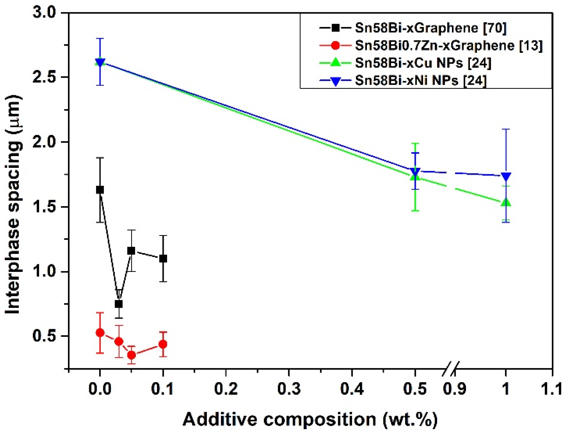
Nanoparticle Addition on the Mechanical Property of the Sn-Bi Solder

The effects of Ag nanoparticle sizes on the mechanical properties of Sn-58%Bi nano-composite solder alloy were studied. Adding Ag nanoparticles to the Sn-58%Bi enhanced the microhardness and reinforced the joint shear strength [121]. The extent of the improvement differed from the size of the doped Ag particles. In this work, the addition of 76-nm Ag nanoparticles generated the best improvement: enhancing the microhardness by 12.2% for the as-prepared solder and reinforcing shear strength by 18.9% after a 180-min liquid reaction at 220 °C. The improvements obtained from the addition of both larger (133 nm) and smaller (31 nm) Ag nanoparticles were much more clear than those for 76-nm Ag nanoparticles. According to Yang et al. [90], 0.05–0.2% Ni-coated carbon nanotubes (Ni-CNTs) reinforced Sn-58%Bi. By the addition of 0.05% and 0.1% Ni-CNT, the microstructure becomes finer when compared to Sn-58%Bi. When 0.05% CNT is added, the tensile strength enhanced by the CNT bridging effect and load transfer, and also creep property of Ni-CNT bearing solders are improved significantly. However, mechanical properties and the microstructure are deteriorated when the content of Ni-CNTs exceeds 0.05%. Shen et al. [27] reported that the elastic modulus and hardness increased with the addition of 0.5–4 wt% of Cu and of Ni nanoparticles to the Sn-58Bi. The enhancement in hardness is significant, in which 4wt% of Cu and Ni addition has increased the hardness of the Sn-58%Bi (287.3 MPa) by 16% and 23%, respectively. The Cu and Ni nanoparticles demonstrate a similar strengthening effect, in which 4 wt% filler addition increases the elastic modulus of the Sn-58%Bi solder (38.4 GPa) slightly by 8–12%. The moduli of the composite solder can be given as Equation (12) [27].
E c = V m E m + kV p E p
where Em and Ep are the modulus of the solder matrix and of the particle (IMC and nanoparticles), respectively. Vm and Vp are a volume fraction of the solder matrix and of particle and K is empirically determined in the range of 0 to 1. With the addition of nano-Cu or Ni to Sn-58%Bi, the creep rate reduces significantly (creep resistance increases) and achieved the best creep resistance when nanoparticle Cu content was 3 wt% and Ni, 1 wt% [27]. Figure 8b shows the shear strength from the literature for various additives to the Sn-Bi solder. It can be seen that the addition of additives up to an optimum level enhances the shear strength of the Sn-Bi solder.
Lee et al. added SiC nanoparticles into Sn-58%Bi solder by electroplating. The shear strength of Sn-58%Bi+nano SiC solder bumps was higher than Sn-58%Bi solder bumps [115]. The increased shear strength was attributed to grain refinement and dispersion hardening by SiC particle dispersion. The amount of Cu diffusion in a Bi-rich phase was higher than that of the Sn-rich phase. According to Li et al., comparing with the monolithic Sn-58%Bi sample, the tensile strength of the composite solders with nano Cu6Sn5 gave lower values but higher elongations and fracture surface changes from brittle to ductile ways. The nano-indentation test shows the creep resistance of Sn-58%Bi-nano Cu6Sn5 is enhanced [91]. Presence of harder nanoparticles can increase the load carrying ability and ehnace the joint reliability [122]. However, due to their high surface energy, nanoparticles increase the probability of agglomeration with each other in the solder matrix. Such non-uniform dispersion and aggregation of nanoparticles degrades the reliability of the solder matrix [123,124,125,126], an optimal content evaluation for each nanoparticle should be made. Strengthening the effect by adding nanoparticles can be obtained by the following factors.
1. Increase of load-carrying ability by the harder nanoparticles than solder matrix ( Δ σ Load ). Solder-containing hard particles is a composite solder and strength of the composite solder is given as a rule of the mixture (13) [122].
σ compo = V p σ p + V m σ m
2. Strengthening by trapped dislocations in the nanoclusters. Restriction of dislocation movement by the nanoparticles, namely Orowan strengthening effect ( Δ σ Orowan ) (14) [123].
Δ σ orowan = 0 . 13 G m b d p [ ( 1 2 V p ) 1 3 1 ] ln d p 2 b
3. Strengthening effect caused by CTE (coefficient of thermal expansion) difference ( Δ σ CTE ) between the solder matrix and nanoparticle (15) [124].
Δ σ CTE = 3 β G m b 12 V p Δ α Δ T bd p
4. Strengthening by the grain or phase refinement (Hall-Petch effect) ( Δ σ Hall Petch ) (7) [125] where k y   and   β are constants, G m is the shear modulus of the matrix, b is the Burgers vector of the pure matrix, V p   and   d p are the volume fraction and diameter of nanoparticles, d m is the grain size of the matrix, σ mo is the yield strength of the unreinforced pure matrix, Δ σ is the CTE difference between the matrix and nanoparticle, and Δ T is the difference between the processing and the test temperatures.

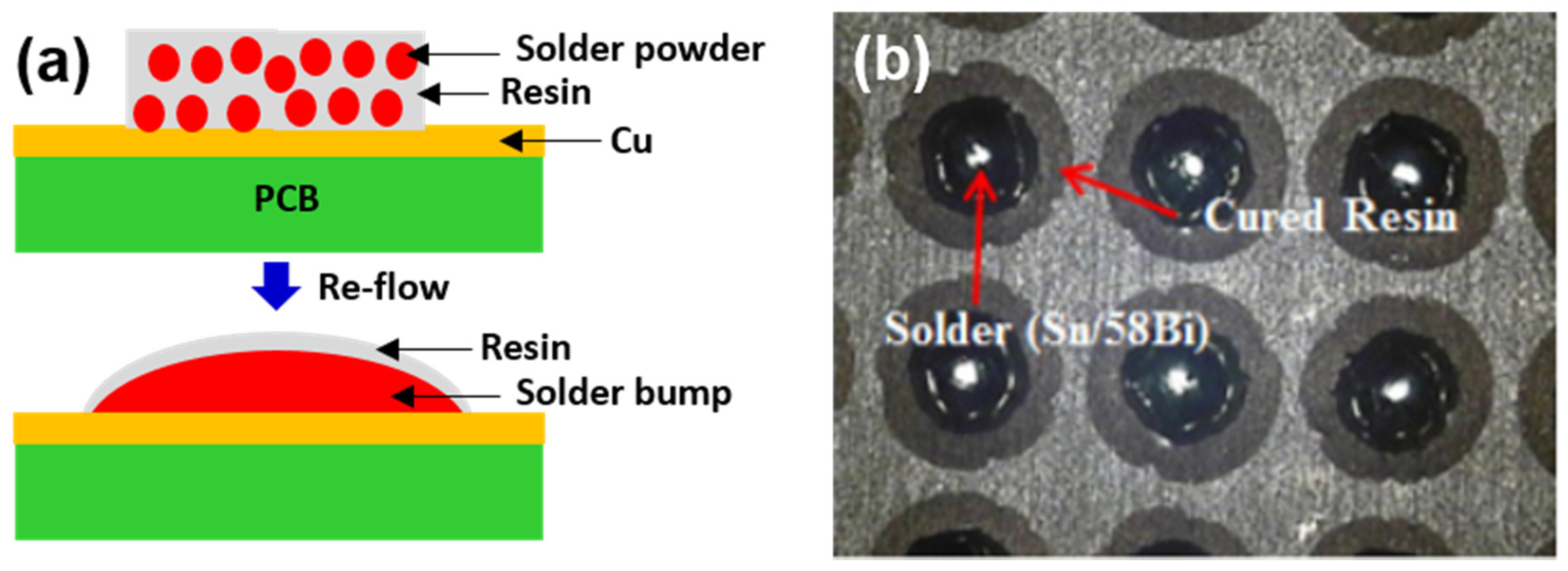
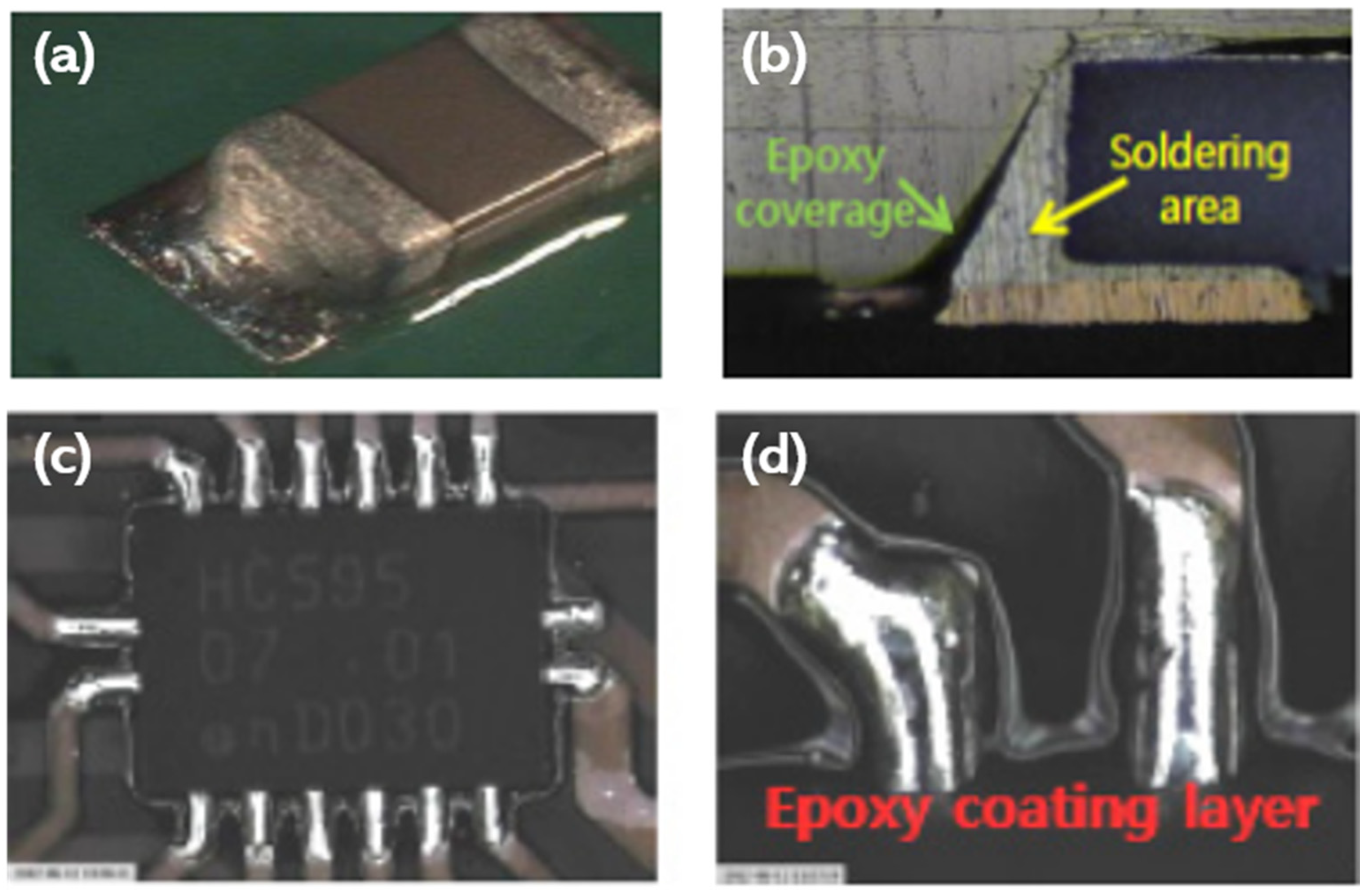
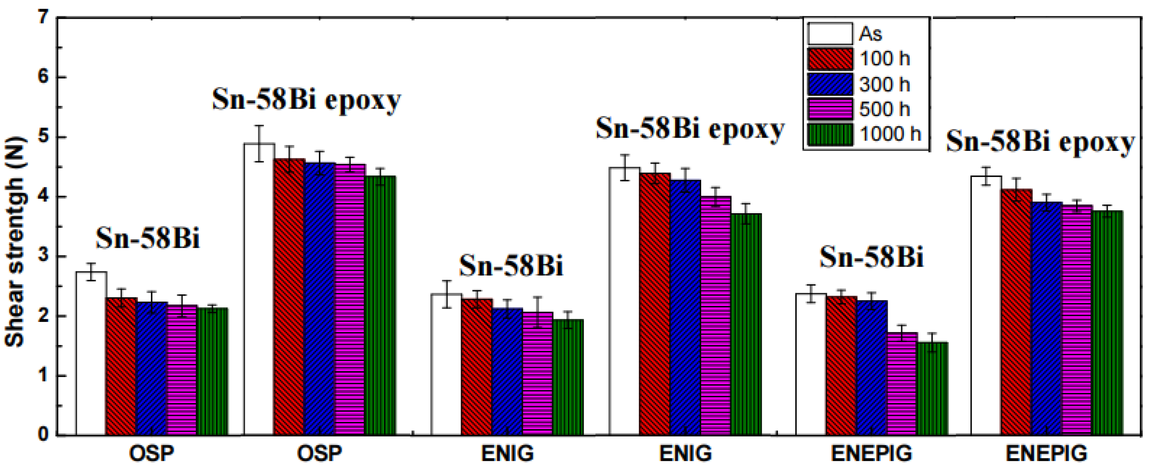
5. Epoxy Reinforced Sn-Bi Solder

Epoxy-containing solder alloys were subjected to numerous studies [30,31,32,33]. Among them, Sn-Bi solder with epoxy is quite meaningful because epoxy can mechanically support low-temperature solder. The advantages offered by epoxy-based bonding solders are as follows [30].
  • The curing temperature of epoxy is much lower than the reflow temperatures of solders (80–150 °C).
  • Joining and curing occurs simultaneously.
  • High reliability during thermal cycling is beneficial for automotive electronics.
  • High surface insulation resistance (SIR) due to the presence of epoxy envelope protects the joint from environmental oxidation.
  • No-clean technology. It provides a clean joint without residues and, hence, washing is not necessary after reflow.
  • The epoxy film over the bumps resides at the necks of the solder bumps and prevents the short-circuiting and corrosion of joints after reflowing.
However, the disadvantages also persist in epoxy-based bonding solders. The bonded structure cannot be easily reworked or disassembled by application of heat and force. In addition, epoxy provides a chemical or mechanical bonding that may have different strength compared to a metallurgical bond. The high rigidity of epoxy joints causes problems in packages with a large die and flexible PCBs. Unavoidably, the CTE mismatch between die and epoxy induce stresses in the solder joint [30]. Yim et al. [32] studied the effect of a reductant concentration on wetting of Sn-58%Bi in the solderable polymer composites (SPCs). Sn58%Bi with 15% epoxy showed excellent coalescence and wetting behaviors for the Cu metallization. Figure 5 shows the reflow temperature profile, schematic soldering, and reflowed bump images of the epoxy solder paste (ESP) containing Sn-58%Bi. When the epoxy solder was reflowed at 150 °C, and Sn-58%Bi powder melted first and wetted on the Cu substrate to form a bump. The resin floated over the melted solder hardened afterward, as shown in Figure 9.
Using the ESP, electronic parts were soldered on PCB, as given in Figure 10. Residue-free clean joints can be observed. Meanwhile, epoxy coating over the solder is confirmed in Figure 10b. Transparent shiney-coated epoxy was observed in Figure 10c,d. The shear force and shear fracture energy of Sn-58%Bi epoxy solder bumps were compared to Sn-58% Bi and SAC305 by K. Kim et al. [117] where the height of the bumps was 180 µm. The epoxy added Sn-Bi solder bumps had asignificantly higher fracture energy than the Sn-Bi solder. This is attributed to the support provided by the epoxy around the fillet. In addition, the epoxy containing Sn-Bi solder has a significant advantage during aging. It was observed that epoxy containing Sn-Bi solder bump can retain a shear strength higher than the monolithic Sn-Bi solder bump even after 1000 h of the thermal cycle, as shown in Figure 11 [117].
Similarly, with the addition of epoxy, the drop property Sn-58%Bi was improved drastically and almost two times of SAC305. It was found that the number of drop impacts coincided with the shear failure energy trend [31]. Lee et al. [29] investigated the drop reliability of epoxy-containing Sn-58%Bi solder joints with various surface finishes in the board level. The presence of epoxy in the Sn-58%Bi solder slightly improved the drop reliability for ENIG and ENEPIG surface finishes compared to the Sn-58%Bi solder joints without epoxy. The presence of epoxy significantly improved the drop reliability for the OSP surface finish. The drop reliability of the Sn-58%Bi joint with the ENIG and ENEPIG surface finishes decreased with an increasing number of reflow, while the drop reliability with OSP surface finishes improved. The drop reliability of the Sn-58%Bi joints with OSP was superior to those with ENIG and ENEPIG due to relatively strong adhesion between the solder/Cu6Sn5 IMC/Cu substrate and the absence of a brittle Ni-P layer in the OSP joint.

6. Conclusions

In this paper, the effect of alloying elements and nanoparticle addition to the low-temperature solder of Sn-Bi was reviewed in terms of melting point, wettability, microstructure, and mechanical properties. Sn-Bi eutectic solder having a lower melting point is useful for poor thermal resisting electronic parts and for reducing the warpage after soldering. The melting temperature of Sn-Bi is not much influenced by Ag, Ti, Co, RE, and ceramic nanoparticles. However, alloying elements have significant effects on the melting temperature. Notably, In addition decreases the melting point but Sb increases. Optimum addition of alloying elements such as Ag, Cu, Sb, and In can improve the wettability of Sn-Bi but excessive addition deteriorates wettability. Sn-rich and Bi interphase spacing and IMC refinement can be obtained with the addition of Ti, Cu, Sb, and ceramic nanoparticles. The Bi-rich layer can be developed along with the Cu-Sn IMC interface of the Cu-substrate after aging and becomes a crack path under stress, which is harmful in terms of reliability. Apart from alloying Ag and Zn, the Ni-P-coated layer on the Cu substrate can reduce the Bi-rich layer production. Tensile strength and elongation can be improved by the optimal addition of nanoparticles. The addition of Zn, Cu, Sb, Ti, and Ni-coated CNTs to Sn-Bi increases tensile strength. Indium increases the elongation remarkably without a significant change in tensile strength. Ag and Zn alloying also enhances tensile strength and fatigue resistance. Epoxy added Sn-58% Bi solder joint can improve shear strength and drop resistance. Sn-Bi eutectic solder extends its application in various wearable and flexible electronic fields. However, drawbacks have to be solved in terms of embrittlement, drop property, bending, and toughness.

Author Contributions

Conceptualization and methodology, H.K. Formal analysis and validation, H.K. and S.H.R. Resources and supervision, J.P.J. Writing—original draft preparation, H.K. Writing—review and editing, S.H.R. and J.P.J. All authors have read and agreed to the published version of the manuscript.

Funding

This work was supported by the Nano-Convergence Foundation (www.nanotech2020.org) funded by the Ministry of Science and ICT (MSIT, Korea) and the Ministry of Trade, Industry and Energy (MOTIE, Korea) (project name: Development of high-ductility, low temperature nano-dispersion solder paste technology for automotive electronics and flexible devices, project Number: R202000210).

Data Availability Statement

Data available on request.

Conflicts of Interest

The authors declare no known financial and personal relationships that could have appeared to influence this work.

References

  1. Abtew, M.; Selvaduray, G. Lead-free solders in microelectronics. Mater. Sci. Eng. R 2000, 27, 95–141. [Google Scholar] [CrossRef]
  2. Johnson, R.W.; Evans, J.L.; Jacobsen, P.; Thompson, J.R.; Christopher, M. The Changing Automotive Environment: High-Temperature Electronics. Ieee Trans. Electron. Packag. Manuf. 2004, 27, 164–176. [Google Scholar] [CrossRef]
  3. Nishida, H. 5G and packaging technology, recent progress/status and items to be considered. J. Jpn. Inst. Electron. Packag. 2019, 22, 596–606. [Google Scholar] [CrossRef]
  4. Gain, A.K.; Chan, Y.C.; Yung, K.C.; Sharif, A.; Ali, L. Effect of Nano Ni Additions on the Structure and Properties of Sn-9Zn and Sn-8Sn-3Bi Solder in Ball Grid Array Packages. In Proceedings of the 2nd Electronics System Integration Technology Conference, Greenwich, UK, 1–4 September 2008; IEEE: Piscataway, NJ, USA, 2008; pp. 1291–1294. [Google Scholar]
  5. Suganuma, K.; Kim, S.-J.; Kim, K.-S. High-Temperature Lead-Free Solders: Properties and Possibilities. Jom Min. Met. Mater. Soc. 2009, 61, 64–71. [Google Scholar] [CrossRef]
  6. Plevachuk, Y.; Hoyer, W.; Kaban, I.; Kohler, M.; Novakovic, R. Experimental study of density, surface tension, and contact angle of Sn–Sb-based alloys for high temperature soldering. J. Mater. Sci. 2010, 45, 2051–2056. [Google Scholar] [CrossRef]
  7. Kamal, M.; Gouda, E.S. Effect of zinc additions on structure and properties of Sn–Ag eutectic lead-free solder alloy. J. Mater. Sci. Mater. Electron. 2008, 19, 81–84. [Google Scholar] [CrossRef]
  8. Gain, A.K.; Fouzder, T.; Chan, Y.C.; Yung, W.K.C. Microstructure, kinetic analysis and hardness of Sn-Ag-Cu-1 wt% nano-ZrO2 composite solder on OSP-Cu pads. J. Alloys Compd. 2011, 509, 3319–3325. [Google Scholar] [CrossRef]
  9. Anderson, I.E. Development of Sn–Ag–Cu and Sn–Ag–Cu–X alloys for Pb-free electronic solder applications. J. Mater. Sci. Mater. Electron. 2007, 18, 55–76. [Google Scholar] [CrossRef]
  10. Liu, L.; Wu, P.; Zhou, W. Effects of Cu on the interfacial reactions between Sn–8Zn–3Bi–xCu solders and Cu substrate. Microelectron. Reliab. 2014, 54, 259–264. [Google Scholar] [CrossRef]
  11. Kotadia, H.R.; Howes, P.D.; Mannan, S.H. On the development of low melting temperature Pb-free solders. Microelectron. Reliab. 2014, 54, 1253–1273. [Google Scholar] [CrossRef]
  12. Jung, J.P.; Shin, Y.E.; Lim, S.S. Pb-Free Micro Soldering, Seoul, South Korea, Samsung Books; 2005; 8p, ISBN 89-88197-43-7. [Google Scholar]
  13. Dongliang, M.; Ping, W. Improved microstructure and mechanical properties for Sn58Bi0.7Zn solder joint by addition of graphene nanosheets. J. Alloys Compd. 2016, 671, 127–136. [Google Scholar]
  14. McCluskey, P.; Munamarty, R.; Pecht, M. Popcorning in PBGA Packages During IR Reflow Soldering. Microelectron. Int. 1997, 14, 20–23. [Google Scholar] [CrossRef]
  15. Singh, A.; Durairaj, R. Study on Hardness and Shear Strength with Microstructure Properties of Sn52Bi/Cu + 1% Al2O3 Nanoparticles. IOP Conf. Ser. Mater. Sci. Eng. 2020, 834, 1–5. [Google Scholar] [CrossRef]
  16. Choi, J.Y.; Park, D.; Oh, T.S. Chip Interconnection Process for Smart Fabrics Using Flip-chip Bonding of SnBi Solder. J. Microelectron. Packag. Soc. 2012, 19, 71–76. [Google Scholar] [CrossRef] [Green Version]
  17. Kim, M.S.; Ko, Y.H.; Yoo, S.; Lee, C.W. Mechanical Properties of Sn-Bi Bumps on Flexible Substrates. In Proceedings of the IEEE 63rd Electronic Components and Technology Conference, Las Vegas, NV, USA, 28–31 May 2013; IEEE: Piscataway, NJ, USA, 2013; pp. 971–975. [Google Scholar]
  18. Chen, X.; Xue, F.; Zhou, J.; Yao, Y. Effect of In on microstructure, thermodynamic characteristic and mechanical properties of Sn–Bi based lead-free solder. J. Alloys Compd. 2015, 633, 377–383. [Google Scholar] [CrossRef]
  19. Shen, J.; Pu, Y.; Yin, H.; Luo, D.; Chen, J. Effects of minor Cu and Zn additions on the thermal, microstructure and tensile properties of Sn–Bi-based solder alloys. J. Alloys Compd. 2014, 614, 63–70. [Google Scholar] [CrossRef]
  20. Wang, Z.; Zhang, Q.K.; Chen, Y.X.; Song, Z.L. Influences of Ag and In alloying on Sn-Bi eutectic solder and SnBi/Cu solder joints. J. Mater. Sci. Mater. Electron. 2019, 30, 18524–18538. [Google Scholar] [CrossRef]
  21. Torres, A.; Hernández, L.; Domínguez, O. Effect of Antimony Additions on Corrosion and Mechanical Properties of Sn-Bi Eutectic Lead-Free Solder Alloy. Mater. Sci. Appl. 2012, 3, 355–362. [Google Scholar] [CrossRef] [Green Version]
  22. Zhou, S.; Yang, C.-H.; Lin, S.-K.; AlHazaa, A.N.; Mokhtari, O.; Liu, X.; Nishikawa, H. Effects of Ti addition on the microstructure, mechanical properties and electrical resistivity of eutectic Sn58Bi alloy. Mater. Sci. Eng. A 2019, 744, 560–569. [Google Scholar] [CrossRef]
  23. Lee, C.-J.; Myung, W.-R.; Park, B.-G.; Jung, S.-B. Efect of Ag-decorated MWCNT on the mechanical and thermal property of Sn58Bi solder joints for FCLED package. J. Mater. Sci. Mater. Electron. 2020, 31, 10170–10176. [Google Scholar] [CrossRef]
  24. Shen, L.; Foo, A.Q.; Wang, S.; Chen, Z. Enhancing creep resistance of SnBi solder alloy with non-reactive nano fillers: A study using nanoindentation. J. Alloys Compd. 2017, 729, 498–506. [Google Scholar] [CrossRef]
  25. Shen, J.; Liu, Y.; Wang, D.; Gao, H. Nano ZrO2 Particulate-reinforced Lead-Free Solder Composite. J. Mater. Sci. Technol. 2006, 22, 529–532. [Google Scholar]
  26. Mavoori, H.; Jin, S. New, creep-resistant, low melting point solders with ultrafine oxide dispersions. J. Electron. Mater. 1998, 27, 1216–1222. [Google Scholar] [CrossRef]
  27. Shen, L.; Wu, Y.; Wang, S.; Chen, Z. Creep behavior of Sn–Bi solder alloys at elevated temperatures studied by nanoindentation. J Mater Sci: Mater Electron 2017, 28, 4114–4124. [Google Scholar] [CrossRef]
  28. Yang, L.; Boqiao, R.; Min, Z.; Xianghua, Z.; Fenglian, S. Microstructure, mechanical, and thermal behaviors of SnBi/Cu solder joint enhanced by porous Cu. J. Mater. Sci. Mater. Electron. 2020, 31, 8258–8267. [Google Scholar]
  29. Lee, S.-M.; Yoon, J.-W.; Jung, S.-B. Board Level Drop Reliability of Epoxy-Containing Sn-58 mass% Bi Solder Joints with Various Surface Finishes. Mater. Trans. 2016, 57, 466–471. [Google Scholar] [CrossRef] [Green Version]
  30. Sharma, A.; Jung, D.H.; Cheon, J.S.; Jung, J.P. Epoxy Polymer Solder Pastes for Micro-Electronic Packaging Applications. J. Weld. Join. 2019, 37, 7–14. [Google Scholar] [CrossRef] [Green Version]
  31. Kim, K.-Y.; Jeong, H.; Myung, W.-R.; Jung, S.-B. Microstructures and Drop Impact Test of SAC305, Sn58%Bi and Epoxy Sn58%Bi Solder Joint on the OSP Surface Finished PCB Substrate. J. Weld. Join. 2018, 36, 14–20. [Google Scholar] [CrossRef] [Green Version]
  32. Yim, B.-S.; Lee, J.I.; Kim, J.-M. Influence of Reductant Content within the Solderable Polymer Composite on the Coalescence and Wetting Behaviors of Low-Melting-Point Alloy Fillers. J. Weld. Join. 2019, 37, 76–81. [Google Scholar] [CrossRef] [Green Version]
  33. Moon, J.-T.; Eom, Y.-S.; Lee, J.-H. Epoxy solder paste and its applications. J. Weld. Join. 2015, 33, 32–39. [Google Scholar] [CrossRef]
  34. Woo-Ram, M.; Yon, G.K.; Kyung, Y.K.; Seung, B.J. Drop Reliability of Epoxy-Contained Sn-58 wt.% Bi Solder Joint with ENIG and ENEPIG Surface Finish under Temperature and Humidity Test. J. Electron. Mater. 2016, 45, 3651–3658. [Google Scholar]
  35. Arenas, M.F.; He, M.; Acoff, V.L. Effect of flux on the wetting characteristics of SnAg, SnCu, SnAgBi, and SnAgCu lead-free solders on copper substrates. J. Electron. Mater. 2006, 35, 1530–1536. [Google Scholar] [CrossRef]
  36. Zang, L.; Yuan, Z.; Zhao, H.; Zhang, X. Wettability of molten Sn–Bi–Cu solder on Cu substrate. Mater. Lett. 2009, 63, 2067–2069. [Google Scholar] [CrossRef]
  37. Yasuda, K.; Shohji, I.; Takemoto, T. Estimation of thermal fatigue resistance of Sn–Bi (–Ag) and Sn–Ag–Bi–Cu lead-free solders using strain rate sensitivity index. Mater. Sci. 2008, 580–582, 221–224. [Google Scholar] [CrossRef]
  38. Amares, S.; Bandar, T. Effect on Shear Strength and Hardness Properties of Tin Based Solder Alloy, Sn-50Bi, Sn-50Bi+2%TiO2 Nanoparticles. Adv. Mater. Res. 2020, 1159, 54–59. [Google Scholar] [CrossRef]
  39. Dong, W.; Shi, Y.; Xia, Z.; Lei, Y.; Guo, F. Effects of Trace Amounts of Rare Earth Additions on Microstructure and Properties of Sn-Bi-Based Solder Alloy. J. Electron. Mater. 2008, 37, 982–991. [Google Scholar] [CrossRef]
  40. Miao, H.W.; Duh, J.G. Microstructure evolution in Sn-Bi and Sn-Bi-Cu solder joints under thermal aging. Mater. Chem. Phys. 2001, 71, 255–271. [Google Scholar] [CrossRef]
  41. Liu, X.Y.; Huang, M.L.; Wu, C.M.L.; Wang, L. Effect of Y2O3 particles on microstructure formation and shear properties of Sn–58Bi solder. J. Mater. Sci. Mater. Electron. 2010, 21, 1046–1054. [Google Scholar] [CrossRef]
  42. Jiang, N.; Zhang, L.; Liu, Z.-Q.; Sun, L.; Xiong, M.-Y.; Zhao, M.; Xu, K.-K. Infuences of doping Ti nanoparticles on microstructure and properties of Sn58Bi solder. J. Mater. Sci. Mater. Electron. 2019, 30, 17583–17590. [Google Scholar] [CrossRef]
  43. Zhang, C.; Liu, S.D.; Qian, G.T.; Zhou, J.; Xue, F. Effect of Sb content on properties of Sn-Bi solders. Trans. Nonferrous Met. Soc. China 2014, 24, 184–191. [Google Scholar] [CrossRef]
  44. Ribas, M.; Kumar, A.; Kosuri, D.; Rangaraju, R.R.; Pritha, C.; Suresh, T.; Siuli, S. Low temperature soldering using Sn-Bi alloys. In Proceedings of the 2017 Surface Mount Technology Association International Conference (SMTA 2017), Rosemont, IL, USA, 17–21 September 2017; SMTA: Eden Prairie, MN, USA, 2017; pp. 201–206. [Google Scholar]
  45. Shalaby, R.M. Effect of silver and indium addition on mechanical properties and indentation creep behavior of rapidly solidified Bi-Sn based lead-free solder alloys. Mater. Sci. Eng. A Struct. Mater. Prop. Microstruct. Process. 2013, 560, 86–95. [Google Scholar] [CrossRef]
  46. Yim, B.-S.; Youn, H.J.; Lee, J.I.; Kim, J.-M. Influence of Carbon Nanotube Concentration on the Interconnection Properties of Solderable Isotropic and Anisotropic Conductive Adhesive. J. Weld. Join. 2020, 38, 152–157. [Google Scholar] [CrossRef]
  47. Ren, G.; Wilding, I.J.; Collins, M.N. Alloying influences on low melt temperature SnZn and SnBi solderalloys for electronic interconnections. J. Alloys Compd. 2016, 665, 251–260. [Google Scholar] [CrossRef]
  48. Dirasutisna, D.T.; Soegiono, B.; Kurniawan, B.; Yudi Masduki, M. Analysis of Thermal Properties of Solder Material Sn-Bi-Al using Differential Scanning Calorimetry (DSC). J. Adv. Res. Mater. Sci. 2016, 18, 1–9. [Google Scholar]
  49. Huang, Y.C.; Chen, S.W. Effects of Co alloying and size on solidification and interfacial reactions in Sne57 wt.%Bie(Co)/Cu couples. J. Electron. Mater. 2011, 40, 62–70. [Google Scholar] [CrossRef]
  50. Šebo, P.; Švec, S.P.; Janičkovič, D.; Illeková, E.; Zemánková, M.; Plevachuk, Y.; Sidorov, V.; Švec, P. The influence of silver content on structure and properties of Sn-Bi-Ag solder and Cu/solder/Cu joints. Mater. Sci. Eng. 2013, 571, 184–192. [Google Scholar] [CrossRef]
  51. Lai, Z.M.; Ye, D. Microstructure and properties of Sn-10Bi-xCu solder alloy/joint. J. Electron. Mater. 2016, 45, 3702–3711. [Google Scholar] [CrossRef]
  52. Miao, H.W.; Duh, J.G.; Chiou, B.S. Thermal Cycling Test in Sn-Bi and Sn-Bi-Cu Solder Joints. J. Mater. Sci. Mater. Electron. 2000, 11, 609–618. [Google Scholar] [CrossRef]
  53. Xu, J.; He, H.; Zhang, F.; Zhao, Z.; Hu, Q. Study of Sn-Bi-Cu Lead-free Solder. In Proceedings of the 10th Electronics Packaging Technology Conference (EPTC), Singapore, 9–12 December 2008; IEEE: Piscataway, NJ, USA, 2008; pp. 1375–1380. [Google Scholar]
  54. Micro-Soldering and Joining Technology; Seoul, South Korea, MPC, Korea Welding & Joining Society, Ace Inc.: Seoul, Korea, 2018; pp. 5–10. ISBN 979-11-89547-00-4. (In Korean)
  55. Wang, K.; Wang, F.; Huang, Y.; Qi, K. Comprehensive Properties of a Novel Quaternary Sn-Bi-Sb-Ag Solder: Wettability, Interfacial Structure and Mechanical Properties. Metals 2019, 9, 791. [Google Scholar] [CrossRef] [Green Version]
  56. Park, J.Y.; Kang, C.S.; Jung, J.P. The analysis of the withdrawal force curve of the wetting curve using 63Sn-37Pb and 96.5Sn-3.5Ag eutectic solders. J. Electron. Mater. 1999, 28, 1256–1262. [Google Scholar] [CrossRef]
  57. Park, J.Y.; Jung, J.P.; Kang, C.S. The analysis of the withdrawal force curve of the wetting balance curve. Ieee Trans. Compon. Packag. Technol. 1999, 22, 372–377. [Google Scholar] [CrossRef]
  58. Park, J.Y.; Ha, J.S.; Kang, C.S.; Shin, K.S.; Kim, M.I.; Jung, J.P. Study on the soldering in partial melting state (1) analysis of surface tension and wettability. J. Electron. Mater. 2000, 29, 1145–1152. [Google Scholar] [CrossRef]
  59. Hong, S.-M.; Park, J.-Y.; Jung, J.-P.; Kang, C.-S. Fluxless Wetting Properties of One-Side-Coated under Bump Metallurgy and Top Surface Metallurgy. J. Electron. Mater. 2001, 30, 937–944. [Google Scholar] [CrossRef]
  60. Hong, S.-M.; Park, J.-Y.; Jung, J.-P.; Kang, C.-S. Fluxless Wetting Properties of Top Substrate Metallurgy in Different Pb-Free Solders. Mater. Trans. 2001, 42, 1423–1427. [Google Scholar] [CrossRef] [Green Version]
  61. Hong, S.-M.; Park, J.-Y.; Kang, C.-S.; Jung, J.-P. Fluxless Wetting Properties of UBM-Coated Si-Wafer to Sn-3.5 wt%Ag Solder. Ieee Trans. Compon. Packag. Technol. 2003, 26, 255–261. [Google Scholar] [CrossRef]
  62. Shin, Y.E.; Lim, S.S.; Jung, J.-P. Soldering, Samsung Books; Samsung: Seoul, Korea, 2002; 13p, ISBN 89-88197-16-X. [Google Scholar]
  63. Takemoto, T.; Makoto, M. Effect of Excess Temperature above Liquidus of Lead-Free Solders on Wetting Time in a Wetting Balance Test. Mater. Trans. 2001, 42, 745–750. [Google Scholar] [CrossRef] [Green Version]
  64. Yang, L.; Zhu, L.; Zhang, Y.C.; Liu, P.; Zhang, N.; Zhou, S.Y.; Jiang, L.C. Microstructure and reliability of Mo nanoparticle reinforced Sn–58Bi-based lead-free solder joints. Mater. Sci. Technol. 2018, 34, 992–1002. [Google Scholar] [CrossRef]
  65. Zhang, L.; Tu, K.N. Structure and properties of lead-free solders bearing micro and nano particles. Mater. Sci. Eng. 2014, 82, 1–32. [Google Scholar] [CrossRef]
  66. Shen, J.; Chen, Y.C. Recent advances in nanocomposite solders. Microelectron. Reliab. 2009, 49, 223–234. [Google Scholar] [CrossRef]
  67. Gain, A.K.; Zhang, L. Interfacial microstructure, wettability and material properties of nickel (Ni) nanoparticle doped tin-bismuth-silver (Sn-Bi-Ag) solder on copper (Cu) substrate. J. Mater. Sci. Mater. Electron. 2016, 27, 3982–3994. [Google Scholar] [CrossRef]
  68. Kang, H.-J.; Kang, J.-W.; Yim, S.-H.; Jung, J.-P. Microstructure and Mechanical Properties of Sn-Bi Solder Reinforced with SnO2 Nanoparticles. In Proceedings of the 6th International Conference on Mathematics, Science, and Education (ICMSE 2019), Semarang, Indonesia, 9–10 October 2019. [Google Scholar]
  69. Ma, Y.; Li, X.; Yang, L.; Zhou, W.; Wang, M.; Zhu, W.; Wu, P. Effects of graphene nanosheets addition on microstructure and mechanical properties of SnBi solder alloys during solid-state aging. Mater. Sci. Eng. A 2017, 696, 437–444. [Google Scholar] [CrossRef]
  70. Vizdal, J.; Braga, H.; Kroupa, A.; Richter, K.; Soares, D.; Malheiros, L.; Ferreira, J. Thermodynamic assessment of the Bi-Sn-Zn system. Comput. Coupling Phase Diagr. Thermochem. 2007, 31, 438–448. [Google Scholar] [CrossRef] [Green Version]
  71. Lee, B.-J.; Oh, C.-S.; Shim, J.-H. Thermodynamic Assessments of the Sn-In and Sn-Bi Binary Systems. J. Electron. Mater. 1996, 25, 983–991. [Google Scholar] [CrossRef]
  72. Vianco, P.T.; Rejent, J.A. Properties of Ternary Sn-Ag-Bi Solder Alloys: Part I—Thermal Properties and microstructural Analysis. J. Electron. Mater. 1999, 28, 1127–1137. [Google Scholar] [CrossRef]
  73. Zhou, S.; Liu, X.; Mokhtari, O.; Nishikawa, H. The Evaluation of Mechanical Properties of Sn58BiXTi Solder by Tensile Test. In Proceedings of the 18th International Conference on Electronic Packaging Technology (ICEPT), Harbin, China, 16–19 August 2017; IEEE: Piscataway, NJ, USA, 2017; pp. 703–707. [Google Scholar]
  74. Sakuyama, S.; Akamatsu, T.; Uenishi, K.; Sato, T. Low Temperature Sn–Bi Soldering Technology for Low Stress Packaging. Ieice Trans. Electron. 2008, 11, 534–541. [Google Scholar]
  75. Mokhtari, O.; Nishikawa, H. Correlation between microstructure and mechanical properties of Sn-Bi-X solders. Mater. Sci. Eng. A 2016, 651, 831–839. [Google Scholar] [CrossRef]
  76. Zhou, S.; Mokhtari, O.; Rafique, M.G.; Shunmugasamy, V.C.; Mansoor, B.; Nishikawa, H. Improvement in the mechanical properties of eutectic Sn58Bi alloy by 0.5 and 1 wt% Zn addition before and after thermal aging. J. Alloys Compd. 2018, 765, 1243–1252. [Google Scholar] [CrossRef]
  77. He, M.; Acoff, V. Effect of Bi on the Interfacial Reaction between Sn-3.7Ag-xBi Solders and Cu. J. Electron. Mater. 2008, 37, 288–299. [Google Scholar] [CrossRef]
  78. Zhai, Q.J.; Guan, S.K.; Shang, Q.Y. Alloy Thermo-Mechanism: Theory and Application; Metallurgy Industry Press: Beijing, China, 1999. [Google Scholar]
  79. Zhang, L.; Tao, W.; Liu, J.; Zhang, Y.; Cheng, Z.; Andersson, C.; Gao, Y.; Zhai, Q. Manufacture, Microstructure and Microhardness Analysis of Sn-Bi Lead-Free Solder Reinforced with Sn-Ag-Cu Nano-Particles. In Proceedings of the 2008 International Conference on Electronic Packaging Technology & High Density Packaging, Shanghai, China, 28–31 July 2008; IEEE: Piscataway, NJ, USA, 2008; pp. 1–5. [Google Scholar]
  80. Lin, D.C.; Liu, S.; Guo, T.M.; Wang, G.-X.; Srivatsan, T.S.; Petraroli, M. An investigation of nanoparticles addition on solidification kinetics and microstructure development of tin-lead solder. Mater. Sci. Eng. A 2003, 360, 285–292. [Google Scholar] [CrossRef]
  81. Lin, D.C.; Wang, G.X.; Srivatsan, T.S.; Al-Hajri, M.; Petraroli, M. Influence of titanium dioxide nanopowder addition on microstructural development and hardness of tin–lead solder. Mater. Lett. 2003, 57, 3193–3198. [Google Scholar] [CrossRef]
  82. Kanlayasiri, K.; Mongkolwongrojn, M.; Ariga, T. Influence of indium addition on characteristics of Sn–0.3Ag–0.7Cu solder alloy. J. Alloy. Compd. 2009, 485, 225–230. [Google Scholar] [CrossRef]
  83. Wu, N.; Ismathullakhan, S.; Chan, Y.C. Effect of 1 wt% ZnO nanoparticles addition on the microstructure, IMC development, and mechanical properties of high Bi content Sn–57.6Bi–0.4Ag solder on Ni metalized Cu pads. J Mater Sci. Mater Electron 2014, 25, 2169–2176. [Google Scholar] [CrossRef]
  84. Gain, A.K.; Zhang, L.; Chan, Y.C. Microstructure, elastic modulus and shear strength of alumina (Al2O3) nanoparticles-doped tin–silver–copper (Sn–Ag–Cu) solders on copper (Cu) and gold/nickel (Au/Ni)-plated Cu substrates. J. Mater. Sci. Mater. Electron. 2015, 26, 7039. [Google Scholar] [CrossRef]
  85. Fouzder, T.; Chan, Y.C.; Chan, D.K. Influence of cerium oxide (CeO2) nanoparticles on the microstructure and hardness of tin–silver–copper (Sn–Ag–Cu) solders on silver (Ag) surface-finished copper (Cu) substrates. J. Mater. Sci. Mater. Electron. 2014, 25, 5375–5387. [Google Scholar] [CrossRef]
  86. Gain, A.K.; Zhang, L. Microstructure, mechanical and electrical performances of zirconia nanoparticles-doped tin-silver-copper solder alloys. J. Mater. Sci. Mater. Electron. 2016, 27, 7524–7533. [Google Scholar] [CrossRef]
  87. He, P.; An, J.; Ma, X.; Chen, S.; Qian, Y.Y.; Lin, T.S. Investigation preparation method and soldering behaviors of Sn-58Bi lead-free solder with carbon nanotubes. Trans. China Weld. Inst. 2011, 32, 9–12. [Google Scholar]
  88. Yang, L.; Zhou, W.; Liang, Y.; Cui, W.; Wu, P. Improved microstructure and mechanical properties for Sn58Bi solder alloy by addition of Ni-coated carbon nanotubes. Mater. Sci. Eng. A. 2015, 642, 7–15. [Google Scholar] [CrossRef]
  89. Li, X.; Ma, Y.; Zhou, W.; Wu, P. Effects of nanoscale Cu6Sn5 particles addition on microstructure and properties of SnBi solder alloys. Mater. Sci. Eng. A 2017, 684, 328–334. [Google Scholar] [CrossRef]
  90. Kang, J. Microstructure and mechanical proerpties of Sn-Bi solder reinforced with SnO2 nanoparticles. Master’s Thesis, University of Seoul, Seoul, Korea, 2019. [Google Scholar]
  91. Li, J.F.; Agyakwa, P.A.; Johnson, C.M. A numerical method to determine interdiffusion coefficients of Cu6Sn5 and Cu3Sn intermetallic compounds. Intermetallics 2013, 40, 50–59. [Google Scholar] [CrossRef] [Green Version]
  92. Onishi, M.; Fujibuchi, H. Reaction-diffusion in the Cu-Sn system. Trans. Jpn. Inst. Met. 1975, 16, 539–547. [Google Scholar] [CrossRef] [Green Version]
  93. Wu, C.M.L.; Yua, D.Q.; Law, C.M.T.; Wang, L. Properties of lead-free solder alloys with rare earth element additions. Mater. Sci. Eng. R 2004, 44, 1–44. [Google Scholar] [CrossRef]
  94. Yoon, J.W.; Lee, C.B.; Jung, S.B. Interfacial Reactions Between Sn-58 mass % Bi Eutectic Solder and (Cu, Electroless Ni–P/Cu) Substrate. Mater. Trans. 2002, 43, 1821–1826. [Google Scholar] [CrossRef]
  95. Wang, F. Interfacial Reaction and Mechanical Properties of Sn-Bi solder joint. Materials 2017, 10, 920. [Google Scholar] [CrossRef] [Green Version]
  96. Liu, P.L.; Shang, J.K. Interfacial segregation of bismuth in copper/tin-bismuth solder interconnect. Scr. Mater. 2001, 44. [Google Scholar] [CrossRef]
  97. Liu, P.L.; Shang, J.K. Interfacial embrittlement by bismuth segregation in copper/tin-bismuth Pb-free solder interconnect. J. Mater. Res. 2001, 16, 1651–1659. [Google Scholar] [CrossRef]
  98. Hu, F.Q.; Zhang, Q.K.; Jiang, J.J.; Song, Z.L. Influences of Ag addition to Sn-58Bi solder on SnBi/Cu interfacial Reaction. Mater. Lett. 2020, 214, 142–145. [Google Scholar] [CrossRef]
  99. Shen, L.; Tan, Z.Y.; Chen, Z. Nano indentation study on the creep resistance ofSnBi solder alloy with reactive nano-metallic fillers. Mater. Sci. Eng., A 2013, 561, 232–238. [Google Scholar] [CrossRef]
  100. Lin, S.K.; Nguyen, T.L.; Wu, S.C.; Wang, Y.H. Effective suppression of interfacial intermetallic compound growth between Sn–58 wt.% Bi solders and Cu substrates by minor Ga addition. J.Alloys Compd. 2014, 586, 319–327. [Google Scholar] [CrossRef]
  101. Wang, F.J.; Zhou, L.L.; Wang, X.J.; He, J.P. Microstructural evolution and joint strength of Sn-58Bi/Cu joints through minor Zn alloying substrate during isothermal aging. J. Alloys Compd. 2016, 688, 639–648. [Google Scholar] [CrossRef]
  102. Yu, X.; Hu, X.W.; Li, Y.L.; Zhang, R.H. Effect of alloying Cu substrate on microstructure and coarsening behavior of Cu 6 Sn 5 grains of soldered joints. J. Mater. Sci. Mater. Electron. 2015, 26, 2782–2794. [Google Scholar] [CrossRef]
  103. Pang, X.Y.; Liu, Z.Q.; Wang, S.Q.; Shang, J.K. Effects of Bi segregation on the tensile properties of Cu/Cu3Sn (1 0 0) interface. Microelectron. Reliab. 2011, 51, 2330–2335. [Google Scholar] [CrossRef]
  104. Shin, H.P.; Ahn, B.W.; Ahn, J.H.; Lee, J.G.; Kim, K.S.; Kim, D.H.; Jung, S.B. Interfacial Reaction and Joint Strength of the Sn-58% Bi Solder Paste with ENIG Surface Finished Substrate. J. Weld. Join. 2012, 30, 458–463. [Google Scholar]
  105. Han, D.Y.; Jing, Y.H.; Nai, M.L.S.; Xu, L.Y.; Tan, C.M.; Wei, J. Interfacial reaction and shear strength of Ni-coated carbon nanotubes reinforced Sn–Ag–Cu solder joints during thermal cycling. Intermetallics 2012, 31, 72–78. [Google Scholar] [CrossRef]
  106. Shimokawa, H.; Soga, T.; Serizawa, K.; Katayama, K.; Shohji, I. Evaluation on Mechanical Properties of Sn-Bi-Ag Solder and Reliability of the Solder Joint. Trans. Jpn. Inst. Electron. Packag. 2015, 8, 46–54. [Google Scholar] [CrossRef] [Green Version]
  107. Mokhtari, O.; Nishikawa, H. Effects of In and Ni addition on microstructure of Sn-58Bi solder joints. J. Electron. Mater. 2014, 43, 4158–4170. [Google Scholar] [CrossRef]
  108. Sakuyama, S.; Akamatsu, T.; Uenishi, K.; Sato, T. Effects of a Third Element on Microstructure and Mechanical Properties of Eutectic Sn-Bi Solder. Trans. Jpn. Inst. Electron. Packag. 2009, 2, 98–103. [Google Scholar] [CrossRef] [Green Version]
  109. El-Daly, A.A.; Ibrahiem, A.A. Influence of rotating magnetic field on solidification microstructure and tensile properties of Sn-Bi lead-free solder. Microelectron. Reliab. 2018, 81, 352–361. [Google Scholar] [CrossRef]
  110. Takao, H.; Yamada, A.; Hasegawa, H. Mechanical properties and solder joint reliability of low-melting Sn–Bi–Cu lead free solder alloy. J. Jpn. Inst. Electron. Packag. 2004, 39, 49–56. [Google Scholar]
  111. Hu, X.; Li, K.; Min, Z. Microstructure evolution and mechanical properties of Sn0.7Cu0.7Bi lead-free solders produced by directional solidification. J. Alloys Compd. 2013, 566, 239–245. [Google Scholar] [CrossRef]
  112. EI-Daly, A.A.; Swilem, Y.; Makled, M.H. Thermal and mechanical properties of Sn–Zn–Bi lead-free solder alloys. J. Alloys Compd. 2009, 484, 134–142. [Google Scholar] [CrossRef]
  113. Lee, C.W.; Shin, Y.; Yoo, S. Effect of SiC Nanoparticles Dispersion on the Microstructure and Mechanical Properties of Electroplated Sn-Bi Solder Alloy. J. Nano Res. 2010, 11, 113–118. [Google Scholar] [CrossRef]
  114. Choi, K.S.; Joo, J.; Jang, K.-S.; Choi, G.M.; Yun, H.G.; Moon, S.H.; Eom, Y.S. Laser-assisted bonding, its bonding materials and their applications. J. Weld. Join. 2020, 38, 138–144. [Google Scholar] [CrossRef]
  115. Bismarck, L.S.; Marcella, G.C.X.; Amauri, G.; José, E.S. Cu and Ag additions affecting the solidification microstructure and tensile properties of Sn-Bi lead-free solder alloys. Mater. Sci. Eng. A 2017, 705, 325–334. [Google Scholar]
  116. Li, J.F.; Mannan, S.H.; Clode, M.P.; Whalley, D.C.; Hutt, D.A. Interfacial reactions between molten Sn–Bi–X solders and Cu substrates for liquid solder interconnects. Acta Mater. 2006, 54, 2907–2922. [Google Scholar] [CrossRef]
  117. Kim, Y. The Improvement of Bonding Strength with an Addition of Epoxy and the Effects of Various Surface Finishes on Sn-58% Bi Epoxy Solder. In Proceedings of the 12th International Symposium on Microelectronics and Packaging (ISMP), Busan, South Korea, 15–16 October 2014. [Google Scholar]
  118. Efzan Mhd Noor, E.; Singh, A.; Tze Chuan, Y. A review influence of nano particles reinforced on solder alloy. Solder. Surface Mount Technol. 2013, 25, 229–241. [Google Scholar] [CrossRef]
  119. Li, Y.; Chan, Y.C. Effect of silver (Ag) nanoparticle size on the microstructure and mechanical properties of Sn58Bi–Ag composite solders. J. Alloys Compd. 2015, 645, 566–576. [Google Scholar] [CrossRef]
  120. Ramakrishnan, N. An analytical study on strengthening of particulate reinforced metal matrix composites. Acta Mater. 1996, 44, 69–77. [Google Scholar] [CrossRef]
  121. Zhang, Z.; Chen, D.L. Consideration of Orowan strengthening effect in particulate-reinforced metal matrix nanocomposites: A model for predicting their yield strength. Scr. Mater. 2006, 54, 1321–1326. [Google Scholar] [CrossRef]
  122. Dai, L.H.; Ling, Z.; Bai, Y.L. Size-dependent inelastic behavior of particle-reinforced metal-matrix composites. Compos. Sci. Technol. 2001, 61, 1057–1063. [Google Scholar] [CrossRef]
  123. Goh, C.S.; Wei, L.; Lee, C.; Gupta, M. Properties and deformation behavior of Mg-Y2O3 nanocomposites. Acta Mater. 2007, 55, 5115–5121. [Google Scholar] [CrossRef]
  124. Ma, D.L.; Wu, P. Effects of Zn addition on mechanical properties of eutectic Sn-58Bi solder during liquid-state aging. Trans. Nonferrous. Met. Soc. China 2015, 24, 1225–1233. [Google Scholar] [CrossRef]
  125. Kubota, Y.; Shohji, I.; Tsuchida, T.; Nakamura, K. Tensile Properties of Low-Melting Point Sn-Bi-Sb solder. In Proceedings of the 16th IEEE Electronics Packaging Technology Conference, (EPTC ’14), Singapore, 3–5 December 2014. [Google Scholar]
  126. Li, J.F.; Mannan, S.H.; Clode, M.P. Interactions between Liquid Sn-Bi Based Solders and Contactmetals for High Temperature Applications. In Proceedings of the 55th Electronic Components and Technology Conference (ECTC ’05), Lake Buena Vista, FL, USA, 31 May 2005; pp. 441–448. [Google Scholar]
Figure 1. Cross-sectional scanning electron micrographs of the flip-chip joints formed by flip-chip bonding of the SnBi solder bumps to the Cu lead frame of the fabric substrate (a) without and (b) with a ball-up process of the SnBi solder paste, reproduced from [16], with permission from Journal of Korean Microelectronics and Packaging, 2012.
Metals 11 00364 g001
Figure 2. Plots of spreading area of Sn-58Bi solder with alloying and nanoparticle addition.
Metals 11 00364 g002
Figure 3. SEM analysis of (a) as-reflow Cu/Sn58Bi/Cu joint, (b) high magnification Sn58Bi microstructure, (c,d) elemental mapping of b corresponding to Bi and Sn, respectively, (e) Sn-Bi phase diagram.
Metals 11 00364 g003
Figure 4. Interphase spacing between Sn-rich and Bi phase for various nanoparticle additions.
Metals 11 00364 g004
Figure 5. Schematic of interfacial inter-metallic compound formed between (a) Sn–58Bi solder and Cu substrate, (b) Sn–58Bi solder, and electroless Ni–P/Cu substrate after aging.
Metals 11 00364 g005
Figure 6. Cross sectional SEM micrographs of the solder joints between Sn-58%Bi solder and ENIG finished substrate after aging at 125: (a) 0, (b) 30, and (c) 100 h [106].
Metals 11 00364 g006
Figure 7. Effect of additives on the IMC thickness of Sn-Bi solder (a) as-reflow IMC thickness as a function of additive composition and (b) IMC thickness for multiple reflows.
Metals 11 00364 g007
Figure 8. Plots for (a) tensile strength of Sn58Bi solder by alloying and (b) shear strength of Sn58Bi solder by a nanoparticle addition.
Metals 11 00364 g008
Figure 9. (a) Schematic diagram of epoxy solder paste bumps reflowed after printing on Cu pads and (b) the actual image of reflowed solder paste bumps, reproduced from [33], with permission from Journal of welding and joining, 2015.
Metals 11 00364 g009
Figure 10. Actual images of devices surface-mounted using epoxy solder paste, reproduced from [33], with permission from Journal of welding and joining, 2015. (a) Capacitor soldered using epoxy solder paste, (b) cross-section of capacitor–epoxy solder joint, (c,d) Integrated circuit (IC) and the high magnification image of IC leg soldered using epoxy soldered paste respectively.
Metals 11 00364 g010
Figure 11. Shear strength of Sn-58% Bi and Sn-58% Bi epoxy solder with various surface finishes and aging time, reproduced from [117]., with permission from ISMP, 15–16 October 2014.
Metals 11 00364 g011
Table 1. Solidus temperature, liquidus temperature, and solidification interval for various Sn-Bi solder alloys.
Solder CompositionSolidus (°C)Liquidus (°C)Solidification Interval (°C)Reference
Sn-58Bi130.21398.8[19]
Sn–58Bi136.1139.13[14]
Sn–58Bi136.1139.13.0[40]
Sn-58Bi139.0143.14.1[22]
Sn-58Bi139.3147.68.3[15]
Sn-58Bi139.5147.68.1[21]
Sn-58Bi139.4148.08.6[16]
Sn-58Bi139.6147.47.8[47]
Sn-58Bi140.3146.05.7[49]
Sn-55Bi1381446[46]
Sn-50Bi13815517[46]
Sn-45Bi13816830[46]
Sn-40Bi13817840[46]
Sn-35Bi13818648[46]
Sn-58Bi-0.5Ti138.9142.73.8[22]
Sn-58Bi-1Ti139.1143.44.3[22]
Sn-58Bi-0.1Ag136.2139.73.5[14]
Sn-57.6Bi-0.4Ag1371425[46]
Sn-58Bi-0.5Ag135.7138.22.5[14]
Sn-58Bi-0.5Ag-0.1RE (RE = Ce and La)136.6139.12.5[14]
Sn-58Bi-1Ag1371425[46]
Sn-38Bi-1Ag13717639[46]
Sn-58Bi-1Ag-1In1331374[46]
Sn-58Bi-1Ag-3In1251338[46]
Sn-58Bi-2Ag139.1145.46.3[47]
Sn-58Bi-2Ag-2In131.2136.04.8[47]
Sn-58Bi-2.0In129.8135.05.2[47]
Sn-58Bi-3.0In119.9140.520.6[15]
Sn-58Bi-4.0Ag138.1145.57.4[15]
Sn-58Bi-3In4Ag116.9138.121.2[15]
Sn-58Bi-0.05Co140.3147.06.7[49]
Sn-58Bi-0.5Co140.1145.04.9[49]
Sn-58Bi-0.1RE (RE = Ce and La)136.2139.73.5[39]
Sn–40Bi–0.1Cu125.1132.27.1[19]
Sn–40Bi–2Zn–0.1Cu.127.7136.38.6[19]
Sn-56.2Bi-3.1Sb139.5147.68.1[21]
Sn-53.2Bi-5.8Sb139.5149.29.7[21]
Sn-52Bi-1.8Sb140.6152.011.4[16]
Sn-44Bi-1.8Sb141.9180.538.6[16]
Sn-48Bi-1.0Sb140.6168.728.1[16]
Sn-48Bi-1.4Sb141.2170.429.2[16]
Sn-48Bi-1.8Sb140.9172.731.8[16]
Sn-48Bi-2.0Sb142.3169.727.4[16]
Sn-48Bi-2.4Sb142.8169.326.5[16]
Sn-48Bi-2.8Sb143.6168.424.8[16]
Sn-20Bi-10In14319350[11]
Publisher’s Note: MDPI stays neutral with regard to jurisdictional claims in published maps and institutional affiliations.

