
A Photovoltaic Technology Review: History, Fundamentals and Applications


1
Department of Electrical and Computer Engineering, Instituto Superior Técnico, 1049-001 Lisbon, Portugal
2
Instituto de Telecomunicações, 1049-001 Lisbon, Portugal
3
Academia Militar/CINAMIL, Av. Conde Castro Guimarães, 2720-113 Amadora, Portugal
*
Authors to whom correspondence should be addressed.
Energies 2022, 15(5), 1823; https://doi.org/10.3390/en15051823
Submission received: 1 February 2022
/
Revised: 23 February 2022
/
Accepted: 25 February 2022
/
Published: 1 March 2022
(This article belongs to the Section A2: Solar Energy and Photovoltaic Systems)
Abstract
:Photovoltaic technology has become a huge industry, based on the enormous applications for solar cells. In the 19th century, when photoelectric experiences started to be conducted, it would be unexpected that these optoelectronic devices would act as an essential energy source, fighting the ecological footprint brought by non-renewable sources, since the industrial revolution. Renewable energy, where photovoltaic technology has an important role, is present in 3 out of 17 United Nations 2030 goals. However, this path cannot be taken without industry and research innovation. This article aims to review and summarise all the meaningful milestones from photovoltaics history. Additionally, an extended review of the advantages and disadvantages among different technologies is done. Photovoltaics fundamentals are also presented from the photoelectric effect on a p-n junction to the electrical performance characterisation and modelling. Cells’ performance under unusual conditions are summarised, such as due to temperature variation or shading. Finally, some applications are presented and some project feasibility indicators are analysed. Thus, the review presented in this article aims to clarify to readers noteworthy milestones in photovoltaics history, summarise its fundamentals and remarkable applications to catch the attention of new researchers for this interesting field.
1. Introduction
1.1. Historical Notes
The photovoltaic effect was first observed in 1839, by Alexandre Edmond Becquerel, a young French physicist. He was conducting electrochemical experiences, when he noticed the occurrence of this effect on silver and platinum electrodes, which were exposed to the sunlight [1,2,3].
In 1873, Willoughby Smith wrote a letter to his friend and colleague Latimer Clark, describing a manifestation of this incredible effect on selenium: “Being desirous of obtaining a more suitable high resistance for use at the Shore Station in connection with my system of testing and signalling during the submersion of long submarine cables, I was induced to experiment with bars of selenium (…). I obtained several bars (…). Each bar was hermetically sealed in a glass tube, and a platinum wire projected from each end for the purpose of connection. (…) While investigating the cause of such great differences in the resistance of the bars, it was found that the resistance altered materially according to the intensity of light to which they were subjected.” [2]. Only 4 years later, in 1877, Adams and his student Richard Day designed and developed the first solar cell. They used selenium, and this device had an efficiency of approximately 0.5%. After one year, Charles Fritts doubled this efficiency, also using selenium but in a different approach: a selenium wafer between two metal thin layers [1,2,3].
Photoelectric theory was proposed in 1905 by Albert Einstein. This theory had some concepts previously proposed by Max Planck. It describes the relation between light waves and photons, which are the quanta of light as well as the relation between the photons energy and its frequency (a linear relation, of which its proportionality constant is the Planck’s one). In 1921, Einstein was award with The Nobel Prize in Physics: “In one of several epoch-making studies beginning in 1905, Albert Einstein explained that light consists of quanta—“packets” with fixed energies corresponding to certain frequencies. One such light quantum, a photon, must have a certain minimum frequency before it can liberate an electron” [4]. According to The Nobel Prize academy, this awards “his services to Theoretical Physics, and especially for his discovery of the law of the photoelectric effect” [4].
High efficiencies were reported when selenium was replaced by silicon. In 1939, Russell Ohl was responsible for the discovery of the the n- and p-type regions in silicon and the photoelectric effect in p-n junctions [5]. This innovation opened doors for the appearance of other technologies, without which we would not have today’s society and knowledge, such as the transistor and the photovoltaic cell (the main focus of this review article). Then, in 1940, Ohl developed on Bell Labs the first silicon solar cell, denominated at that time as light-sensitive electric device [6].
In this first experiments, all these researchers and inventors reached a unique conclusion: the generated current is proportional to the incident radiation and this proportionality depends on the radiation wavelength. However, instead of being used as solar cells (due to its low efficiency), these devices were used as sensors [1,2,3]. An awesome example was the photography light sensors developed by the German engineering Werner Siemens, the founder of Siemens [2]. He was the first to commercialise such unique devices, not as photovoltaic cells, but as those sensors.
Despite this, only in 1954, Calvin Fuller, a chemist from Bell Labs, developed a process to dope silicon [1,2,5]. This innovation led to the creation of the first p-n junction (diode), a work signed by the physicist Gerald Pearson, Fuller’s colleague, who helped create it, by immersing a doped silicon bar on lithium. They reported photovoltaic properties and an astonishing efficiency of 6%, for dopants of boron and arsenic [1,2].
In 1955, a solar cell was placed as the power source of a telecommunication network in Americus, Georgia. This is the first ever application of a solar cell, about one year latter of the device’s presentation on an annual meeting of the USA National Academy of Sciences, held in Washington on 25 April 1954 [1,2,5].
Other applications came up extraordinarily fast. On 17 March 1958, NASA launched a satellite named Vanguard-I, which was the first one to have a solar system. Vanguard-I was equipped with two transmitters, one using a mercury cell source an the backup one using a solar system composed by six silicon solar cells. They worked eight years, which is an excellent progress, since the conventional mercury power system had a lifetime of twenty years [1,2]. NASA was not initially convinced about the advantages and future necessity of having a solar power system on their extraterrestrial products. However, photovoltaic technology was getting its opportunity, as several missions were successful due to this new way of producing power. Only two months later, the Russian space program launched its satellite Sputnik-3, also having a photovoltaic solar source. Thenceforth, photovoltaic power sources are an important system on spacial projects [1,2,7].
It goes without saying that the war to discover space was one of the great drivers for the advancement of the photovoltaic technology [1,7]. Public applications were always a goal to be reached. However, the lack of optimised manufacture processes and consequently the expensive commercialisation cost were the main barriers to this advance.
On 1970s, a worker of Communications Satellite Corporation (Comsat) named Joseph Lindmeyer developed a process that increases the efficiency of silicon solar cells by 50%. Lindmeyer left the company and together with Peter Varadi founded Solarex in 1973, with the aim of developing solar cells for public applications. Despite the patent of this process being owned by the Comsat and not by Lindmeyer or Solarex, in 1980 Solarex had approximately 50% of the photovoltaic industry market. It was a small market, but it was increasing since 1973 (several months after Solarex foundation) due to the oil crisis [1,2].
Driven by this crisis, the scientific community interest for photovoltaic technology rose. New technologies appeared, using different and new materials, aimed at the reduction of manufacturing costs. Until 1973, mono-Si (monocrystalline silicon) was used, but thereafter poly-Si (polycrystalline silicon) and a-Si (amorphous silicon) drove the market, since their processes were much cheaper and less demanding [1,2,8].
From thereon, photovoltaic technology has been improved with other techniques. New solar cells appeared, having the necessity of categorising cells in two, and later on, three different generations [8,9,10]. Nowadays, some researchers and manufactures request a new division, creating the fourth one. These generational categorisation stems from the materials and techniques used in their production, as it is possible to verify in this article as well [9,10,11,12].
Moreover, the discovery of other phenomena on other interesting areas such as electronics, photonics or quantum mechanics allowed the improvement of photovoltaic cells. It is already possible to have flexible solar cells and even painted solar cells [11,13,14,15]. The improvement of different cells’ efficiency is presented by National Renewable Energy Laboratory (NREL) in [8]. This chart is commonly presented and cited in several research works and it is grouped and updated by the NREL. “NREL maintains a chart of the highest confirmed conversion efficiencies for research cells for a range of photovoltaic technologies, plotted from 1976 to the present” [8]. This chart will be addressed on the following sections. The comparison among different technologies and generations will be performed after, but it is already noticeable that photovoltaic technology research area has been an interesting field along all these decades, namely on the past decade, since more milestones/marks appear on the NREL chart.
On the top of that, a photovoltaic system started to be seen not only as the photovoltaic cells, but also with other elements such as inverters, batteries, and even the cables to connect these components [16,17,18,19]. Every improvement in any of these devices led to the improvement of the system efficiency and consequently to enhance advantages of photovoltaic technology.
1.2. Current Commitments and Goals
Nowadays, photovoltaic technology overcame all the expectations. Photovoltaic panels are everywhere. Some technologies are now massively produced, leading to manufacture cost reductions.
In today’s projects, other variables are taken into account: besides the financial viability, the environmental “costs” are also analysed. Presently, photovoltaic panels are so easily brought for public applications that the key is no longer how to produce energy (as in the 20th century), but it is how to produce green energy. This means that the produced energy should be have a smaller ecological footprint in comparison with any other way of producing it (usually compared with fossil fuels sources). One way of measuring this ecological footprint may be by the ratio of CO2 per produced power during all the source lifetime (since the manufacturing up until the recycling) [9,20,21,22,23].
Similarly to the advances felt on the manufacture processes, photovoltaic industry is expectant for innovation and novelties about the recycling processes.
The world is constantly changing, nonetheless energy production is still dominated by the non-renewable sources, mainly fossil fuels. However, new energy sources are competing with the fossil fuels, allowing us to make our planet a better place to live. Low emissions of toxic gases during all the manufacture, working and recycling periods in comparison with non-renewable energies, make renewable source a quite interesting alternative. In this group, photovoltaic technology has the biggest potential, because it is cheap and easy to set [9,10,16,24,25].
Climate change concerns and the incredible, increasing, demand of our societies, caused by the ever growing of our population, require an enormous effort to shift from conventional energy production methods and turn to renewable energies [18,19,26].
The European Commission wrote in its proposed European Green Deal the promise of cutting greenhouse gas emission by at least 55% until 2030 and the expectation of being neutral by 2050 [18,19].
Additionally, the United Nations established its Sustainable Development Goals (SDGs) in 2015, in a document entitled “Transforming our world: the 2030 Agenda for Sustainable Development”. The simplest way to show the transforming capability of photovoltaic technology is looking at these goals. On a total of 17 goals, photovoltaic technology can be easily associated to three of them: 7th (Affordable and Clean Energy), the 11th (Sustainable cities and Communities) and the 13th (Climate Action) [27].
2. Photovoltaic Generations
Solar cells are usually classified into generations, as exemplified in Figure 1, this categorisation stems from the materials and techniques used in their production [12]. The first generation is wafer-based, meaning that the core of their fabrication techniques were built upon techniques already employed at the time for integrated circuit manufacturing, allowing them to reap the benefits from the large expertise in the field of silicon wafer production [12]. In the photovoltaic module universe, this first generation is still the most prevalent, accounting for 95% of produced power in 2020 [16]. Second generation cells were developed with the intent of reducing the costs of the previous generation and improving their characteristics.
A good metric to maintain in photovoltaic module production is that the overall cost of the module is half of its installation cost, and that the cost of the cells, are likewise less than half of the module [28]. From this, a logical way to achieve a cheaper module was to reduce the high material demand of the cells, and the inherent cost associated. The second generation of cells is then based on thin film technology, marked for their thin absorber layer. In the order of a couple μm, rather than 100–200 μm of the previous generation. The trade off, however, was a decrease in efficiency. With a thin substrate the efficiencies of the previous generation could not be achieved at first. But counterpointing the efficiency decrease is ability to utilise other manufacturing techniques such as spray coating into a thin glass substrate, and other vacuum based methods, requiring overall lower temperatures in its production process. Their flexibility, that opened up several new possible applications for photovoltaic cells, such as wearable electronics [13]. Additionally, in comparison, their reduced energy payback time and green house gas emission [29] make them an environment friendlier solution. Currently, the initial efficiency drawback is no longer prevalent, as values above 20% were achieved, with a present record of 23.4% [8].
Third generation photovoltaic cells were built upon thin film technology, but diverged from the previous, as it was no longer reliant on a standard p-n junction [12], in the sense that they were built with new and different materials such as organic compounds, hence the name. Another great improvement achieved in this generation was the ability to tune band gap energies with composition changes, a key factor in the production of multi junction cells.
Another interesting point that could be made, regarding solar cell generations, is that even though technologies share certain aspects between them, especially in the same generation, the efficiency achieved and interest in cell type vary. Therefore a metric can be devised to compare research interest and investment. Extracting the efficiency breakthroughs for each cell type from the NREL chart [8], comparing it with the time frame, a certain Research Tendency (RT) is noted. As usually, records in efficiency are correlated with breakthroughs in fabrication techniques, that are only possible if there is sufficient research on the topic. However, RT alone is not sufficient to assess research interest presently, as a technology could have had several breakthroughs and than stalled its improvement. Therefore, another complementing metric is added, , that acts much like RT, but regarding only the last 5 years. These metrics, when applied to NREL’s efficiency chart [8] lead to Table 1.
2.1. First Generation
Silicon Solar Cells
From the historical notes sections it is clear that Silicon solar cells have been present for quite some time. And even with the development of several alternatives to Silicon based photovoltaic cells, it remains as the most widespread and prevalent photovoltaic technology today [16]. Silicon is one of the base materials of the first generation solar cells. Two key factors that contribute for this supremacy is the attractive bandgap energy of Silicon, at 1.17 and the abundance of high quality material, due to an already scaled silicon based semiconductor production for microchips [30].
To understand the relevance of bandgap energy and its correlation with solar energy conversion it is necessary first to acknowledge some characteristics of light emitters, in this case stars. In astrophysics, when a new star is found one of the first studies conducted is of its emission spectrum, as it contains valuable information regarding its composition and temperature. Each element produces a unique emission spectrum, a band spectrum, with each band representing the band energy values of the element. Additionally, as temperature is linked with particle excitation, the higher the temperature the higher the particle excitation and that, in essence, reflects particle energy. Taking then the visible light spectrum as reference. A star with higher surface temperatures will emit a spectrum with a peak shifted towards the blue side of the visible spectrum, giving it a blue hue. A colder star, in comparison, will have its emission peak towards the red side of the visible spectrum, conferring it a red hue. In the case of the Sun’s emission spectrum, its peak is in the visible region towards green at a wavelength of 520 , with good prevalence in yellow and red wavelengths as well.
In photovoltaic design, the bandgap of the semiconductor absorber defines a range where the material is efficient at converting the incident photons into charge carries. This, in combination with the Sun’s emission spectrum determines a range for semiconductor bandgap energies if a good conversion efficiency is to be expected. In homojunction devices, this range corresponds to 1.1 to 1.7 . Silicon, with 1.17 is not at the maximum, of around 1.4 , but within this range. Yet, its efficiency is diminished since Silicon is an indirect bandgap semiconductor, meaning that there is a difference in momentum between the edges of the conduction and valence band. This difference in momentum, translates to increased thermalization losses through energy dissipation to the lattice structure of the semiconductor during recombination. With Auger recombination as the prevalent intrinsic recombination process [31]. So a direct semiconductor with a higher bandgap value would be preferable for photovoltaic energy conversion. Additionally, here is where the microchip industry had a big part in determining the future of photovoltaic cells.
With an already scaled production of high grade silicon wafers, the cost of silicon was more advantageous than developing a dedicated semiconductor production for photovoltaic cells even if Silicon characteristics were not the ideal. Moreover, wafers of lower grade Silicon, that could not be used for integrated circuits, could be purchased at lower cost by the photovoltaic industry. As such, semiconductors with more attractive attributes, for example GaAs, were limited to applications were specific qualities where of greater importance than cost, as in space, for power sources of satellites.
Since its appearance, crystalline Silicon (c-Si) photovoltaic cells have increased in efficiency 20.1%, from 6% when they were first discovered to the present efficiency record of 26.1% [8]. The advances in semiconductor production, needed to increase computing power of microprocessors, had a direct impact in increasing photovoltaic conversion efficiency, as bulk defects were progressively eliminated in wafers. However, good bulk quality is just one requirement for high efficiency cells, there are other factors that limit module efficiency, so other type of fabrication breakthroughs are also credited for the increase in efficiency over the years. Notable breakthroughs were, at wafer processing, multi-wire sawing that allowed for a reduction in material lost, decreasing the overall cost of the cell [30,31]. Block casting that, even though it results in lower grade wafers of polycrystalline silicon, is cheaper to produce and assemble into modules [30,31]. Surface texturing, of the top and bottom surfaces to reduce reflection [30,31,32]. The introduction of an aluminium back surface (Al-BSF) to decrease rear surface recombination velocity [30,31,33]. Additionally, the development of passivated emitter and rear cell (PERC), to further reduce rear surface recombination velocity [33,34].
Currently, crystalline silicon cells are responsible for 95% of the global photovoltaic energy production [16], so their prevalence is clear. However, with the demonstrated increase in efficiency of thin film solar cells, closely matching c-Si with the added benefit of reduced semiconductor costs, this figure is expected to change. Moreover, complex architectures based on heterojunctions have already surpassed c-Si homojunction efficiency records, and assuming a reduction in production cost as the technology and related processes get more streamlined, they could play an important role in the future of photovoltaics.
2.2. Second Generation
Cigs
Since Si, the cornerstone of the photovoltaic market has decreased in price in the latter years, [35,36], new competing technologies have had a hard time gaining a substantial market presence. To compete with the standard technology, the focus then should be to target the costly aspects of Si module production and to cater to different applications. A key aspect to improve comes from reducing the high semiconductor material dependency and the overall balance of system costs. This was the driving force that led to the appearance of the second generation of photovoltaics with the use of thin films, which CIGS are part of [9,10].
Chalcopyrite thin films for solar cells stem from earlier works into development of GaAs LASER photodetectors, where a full spectrum quantum efficiency measure of a CdS/CuInSe2 heterojunction pointed to a possible solar cell application [37]. Additionally, with some modifications, it yielding an initial efficiency of 12% [37,38]. Copper indium gallium (di)selenide (CIGS), appeared at a later stage, with the introduction of wider band gap materials in existing thin films, CuInS, in an attempt to increase the open circuit voltage [39]. The introduction of Ga enabled band gap tailoring by varying the Ga and In composition ratio in a range of 1.0 eV, in pure CuInSe2 to 1.7 eV, in pure CuGaSe2, usually appearing in a grading in high efficiency cells [40].
The lower band gaps achieved with composition tailoring, notably the 1.0 eV to 1.1 eV range, opens an attractive route for future applications, as a bottom cell in tandem architectures. A more in-depth description of multijunction and tandem architectures is conducted further ahead, but in principle in a tandem architecture two or more junctions with different bandgaps are stacked in order to increase overall efficiency, by, in essence, segmenting the solar spectrum with each junction tailored to absorb one of these segments. So, the low bandgap of CIS and CIGS makes them ideal candidates for tandem architectures, but further research is still needed in this aspect [40], since currently the record efficiency for a Perorvskite/CIGS tandem is of 18% [8].
In terms of CIGS manufacturing, the standard fabrication process consists of several stages of sputtering deposition followed by mechanical or LASER scribing. Firstly, a layer of molybdenum is deposited on usually a glass substrate by a sputtering process, forming the back contact. Then, the first stage of patterning, followed by deposition of the CIGS absorber layer either by co-evaporation or sputtering, finished with selenazation and sulfurization of precursors. After, a buffer layer is introduced, usually of cadmium sulphite. Lastly, a TCO layer at front contact is applied to reduce current leakage followed by an anti-reflective coating. A further description of this process can be found in literature, such as [9,40,41,42].
Considering the techniques used in production, a cost reduction can be achieved, with the use of alternative production processes as roll to roll processing (R2R). In the case of CIGS, R2R processing consists in a continuous sublayer of polymer on which the subsequent layers are deposited to form the CIGS [14], in a process much like the described earlier, only in this case on a continuous flexible substrate. With this technique, large scale production of CIGS is feasible, and given that the end product are strips of flexible series connected cells, that can later on be integrated in rigid or flexible modules, depending on encapsulation, it allows for a multitude of applications.
There is already a company that makes use of R2R processing, Flisom. The versatility in integration of the strips is exemplified in their product line, with a standard hard module of 100 Wp, a flexible module of 165 Wp and lastly the strips themselves that allow for a custom range of power and voltage [15]. Additionally, given the possibility of delivering a roll of cells up to 3.5 , projects such as BIPV (Building Integrated Photovoltaic), automotive and railway integration, that require large areas of solar arrays, become much more feasible. Moreover, CIGS modules with flexible encapsulation are lighter than standard Si modules, therefore the weight of modules, the weight of the supporting structure and installation time required is reduced as well [9,10].
In terms of efficiency, the record for CIGS is 23.4% by Hemholtz-Zentrum Berlin, a figure that rivals with the best Si cell efficiencies [8]. It should be noted however that research cell efficiencies do not have a direct translation to industrially achievable efficiencies, due to the nature of large scale processing. Nonetheless, module efficiencies above 20% are already a reality [9]. The efficiency increase of CIGS cells has been remarkable in the last years and further increases are expected, following further studies into post deposition Alkali treatment [40], for example.
2.3. CdTe
Cadmium Telluride, the absorber of CdTe solar cells, is a direct bandgap material with an energy value of 1.5 , ideal characteristics for solar energy conversion. The first prototype of a CdTe cell is credited to Bonnet and Rabenhorst in 1972, after demonstration of a working device with 6% efficiency [43]. This figure has, since then, increased considerably, with the current record value for research efficiencies at 22.1% by First Solar in 2015 [8]. The increase in efficiency has not been steady along the years and can rather be credited to several fabrication breakthroughs, remaining fairly stagnant in between. Nonetheless, the technology is still attractive, especially given that it represents the biggest percentage of thin film modules and has had significant increases in its production at the global scale in the latter years [16].
Since Cadmium is a natural by-product of zinc refinement, CdTe cells appear as a way to repurpose an already existing waste into a form of renewable energy production. A strong argument in favour of its production. However, there are some environmental concerns regarding the environmental impact of the cells and safety during production as cadmium is an extremely hazardous heavy metal with known carcinogenic and mutagenic properties as well as long lasting toxic effects for aquatic life [44]. Additionally, tellurium, even though not as toxic, still poses an environmental concern to aquatic life and, much like cadmium, can be fatal if inhaled [45].
In terms of the environmental impact concerns, these boil down to chemical leakage from damaged cells and modules that could lead to heavy metal accumulation in water basins or soils and the subsequent poisoning that it would ensue, or alternatively the air born release of cadmium and tellurium if a fire occurs [43]. As such, several studies have been conducted to assess the true environmental impact and concerns regarding cadmium telluride, where it was found that the compound was comparatively less toxic and more stable than the pure elemental form of its constituents [43,46,47], and that in normal conditions and foreseeable accidents could be considered a safe way to sequester the oversupply of cadmium [47].
Regarding CdTe cells, there two main configurations, substrate and superstrate. In a superstrate configuration, the layers are usually deposited on a soda-lime glass substrate, with the first deposited layer serving as the front contact. With this configuration, the base substrate needs to be transparent, a key difference to its alternative, where there is more leeway in terms of substrate choice. In a substrate configuration, the layer sequence is inverted, so the base substrate can be a metal foil or opaque polymers, an ideal characteristic for the development of flexible CdTe cells since it’s harder to find good conductive transparent materials for encapsulation. However, despite its apparent constraints, the superstrate configuration has achieved the highest efficiencies to date [43].
Currently, the main constraint of CdTe cells is the open-circuit voltage (explained below, on electrical models section) that cripples the efficiency of the cell. Some variations of CdTe cells have already demonstrated an increase in voltage, obtained through phosphorous doping, but there was a significant decrease in current, therefore the overall efficiency did not increase [48]. However, this poses a possible route to increase efficiency in the future if the current loss can be mitigated [48]. Since the theoretical efficiency limit for single crystalline CdTe is around 33% [47], there is clearly room for improvement.
Another interesting capability of CdTe is their reduced dimensions, with its great spectral efficiency the absorber thickness could be reduced to around 1 μm without major losses in efficiency [43], although more work is needed. Super thin cells are especially attractive for flexible applications and BIPV due to their reduced weight, and with the choice of transparent encapsulation, clear CdTe photovoltaic panel can be developed. Their transparency varies from around 10% to 50%, with the drawback that increasing transparency decreases necessarily the efficiency. Nonetheless, transparent panels could be a substitute for window panels in building, not only generating electricity that could be used to power themselves but contributing for noise reduction and thermal isolation [19], as most panels are double glass encased. Moreover, if space is of constraint, as is in the case of an island, the introduction of transparent CdTe cells could be a good solution to consider [18].
2.4. Third Generation
2.4.1. Multi-Junction
The intrinsic properties of the semiconductor base chosen, such as bandgap energy and carrier recombination velocity, represent inherent limitations to the performance of the cell. Consider silicon, the most prevalent material in photovoltaic cells, it has a band gap energy of approximately 1.11 , therefore only incident photons of equal or higher energy value will lead to the formation of charge carriers, and even so there are still thermalisation and recombination losses to consider. As only part of the solar spectrum meets the needed energy requirements for carrier formation, for a given semiconductor, the limitation becomes apparent. This limit, with an estimation of 29.4% [33,49], for silicon-based homojunction solar cells is the well known Shockley–Queisser limit.
With the objective of reducing thermalisation losses and increasing efficiency, several approaches can be considered. One approach would be to tailor the incident radiation with a specific material, for example by using a prism and pairing each band with the adequate substrate. This approach, even though used in some concentrator photovoltaic devices like a photovoltaic mirror or a spectral splitting device like a dichroic mirror [50], is not a common and practical solution.
A common solution is the multi-junction or tandem architecture, that consists in stacking different substrates with decreasing band gap energies, from top to bottom, so that photons of decreasing energy values are absorbed by the different layers as they penetrate the cell structure, thus achieving a sort of band selectivity [7,28,51,52]. With this solution, it is possible to overcome the previous value of the Shockley–Queisser limit. The theoretical maximum efficiency value of this architecture is approximately 85% for an infinite number of junctions with perfect substrate pairing [53,54] under concentration, and to approximately 65% under one sun [52,53,54].
For multi-junction cells, even though band gap energy is of paramount importance in the choice of materials for the layers, the lattice constant of each one must be considered as well, as the production of a stack with materials with different lattice constants can lead to dislocations in the structure, which promote the appearance of nano fractures in the grid and cause parasitic losses, compromising performance. To reduce these effects, compositionally graded buffers (CGB) are introduced between mismatched layers so that the transition is smoothed, and this is achieved by varying the composition of the buffer layer along its thickness so that it better matches the lattice constant of the two junctions at the extremities, albeit small dislocations are still present [55]. One would think that there is no advantage in producing lattice mismatched devices, since not only is the fabrication process harder and material quality must also be partly compromised, however, the introduction of lattice-mismatched junctions is a flexible direction for achieving the desired bandgaps and opens the possibility of utilising a larger selection of materials.
In terms of nomenclature, when a multi-junction device has all the layers with the same lattice constant, it is known as lattice matched, otherwise it is lattice mismatched or metamorphic [7].
Stacked structures are usually monolithically grown in a substrate with the layers connected in series by tunnel junctions. If the process starts from the layers with the highest band gap energies towards the lowest, then the structure is grown in an inverted manner. This would be the preferred process, for example, if the top layers were lattice matched and the rest were not, achieving therefore a inverted metamorphic multi-junction device [51,52]. In the lattice matched case, the layers would be deposited in a thin substrate of low band gap energy that would serve as the bottom junction. The latter has the advantage of requiring fewer steps to completion, since in the case of the inverted configuration a handle must be bonded for structural support to then remove the substrate on which the structure is grown. The costs of these extra steps can be mitigated however, as the removed substrate can, in some cases, be recycled or reused [52].
The other approach to building stacked structures is by mechanically stacking the sub-cells and bonding them with transparent conductive bonds. This approach has the advantage of individually fabricating the sub-cells, ensuring the perfect conditions for cell growth.
The selection of the fabrication process is linked to the desired terminal configuration. There are two main design types, two-terminal and four-terminal [33,50]. In the second case, the mechanically stacked approach is required in order to obtain the four external terminals, two from each sub-cell. The two-terminal configuration is achieved usually by monolithically growing the cell.
In the two-terminal configuration all the layers are connected in series, this poses some technical challenges as the output current of the device is limited by the junction with the lower value. Not only that but the fabrication process introduces more challenges since each material require certain conditions in order to maintain their properties, and by monolithically growing the layers careful manipulation is required in order to preserve them, making the overall process laborious. This is not the case however for the four-terminal configuration, as the top and bottom sub-cell not only are grown separately, but can also be operated independently from each other, reducing the cell’s sensitivity to spectral variations. Nonetheless, the two-terminal configuration may still have some advantages in terms of efficiency, assuming an optimisation of the optical properties of the sub-cells is achieved, since the transparent bonds used for stacking, the additional transparent contacts still introduce significant parasitic absorption losses [33] and, hand in hand with the freedom that the additional contacts provides, comes the added cost of the necessary control electronics.
2.4.2. Perovskite
The first prototype of a halide perovskite-based solar cell was first demonstrated in 2009, with a conversion efficiency of 3.8% [28,50,56,57]. Regardless of its low efficiency at the time, the prototype sparked an interest in the technology, and the research that followed was fuelled by the pursuit of a cheaper non-silicon based photovoltaic cell.
Halide perovskites have an ABX crystalline structure, pictured in Figure 2, where A and B are cations, with +1 and +2 charge respectively, and a X anion, with charge. The distinct advantage that perovskite has is the ability to replace in its structure the halide component, X, and A cation to obtain different band gap energies, while maintaining a tolerance factor that ensures a stable crystalline structure [56]. With this property, a multitude of pervoskite materials can be synthesised, with bandgap energies in the range 1.5 to 3 .
This bandgap tunability with compositional changes makes perovskite an ideal candidate for heterojunction applications, especially in tandem architectures. Carefully tailoring the band gap energies of each substrate is a key factor in tandem photovoltaic cell design. Therefore, perovskite can be a way to undercut cost, by substituting costly layers while maintaining the desired bandgap.
A full tandem perovskite structure is a rather different challenge, since low bandgap energy perovskite is still lacking. A recent improvement in fabrication techniques allowed for the development of perovskite with bandgap energies in the range 1.2 to 1.3 , leading to a laboratory efficiency record of 21% on a four terminal tandem architecture [58]. A two terminal solution poses a more complex problem in terms of processing and layer bandgap restriction, as denoted by its record efficiency of 17% at the moment [58]. Pairing perovskite with another type of substrate, as Si, creating the so-called Hybrid tandem, would allow the architecture to reap the benefits of the already established technology as well as the lower bandgap energy of Si, while improving the overall efficiency.
A hybrid solution, as described earlier, would retain some of the cost benefits of thin film processing and could potentially lead to an efficiency cost solution better than III–V compounds based tandems, as even though they are the record holder in terms of cell efficiency, but are also extremely expensive, limiting them to space applications where performance, rather then cost, is the main factor of choice.
There is still a long way to go until a viable commercialisation of the technology, since several factors plague the lifetime of the cell, jeopardising module feasibility. Due to the nature of the compounds used, especially in organometallic hybrids, the cells are sensitive to oxidation and humidity, resulting in cells with unstable performances, as evidenced in [59], where in the span of approximately one month, degradation of the perovskite materials could easily be observed. Additional steps in cell encapsulation can mitigate these reactions, but represent a costly addition. A common perovskite hybrid, CH3NH3PbI3, that showed great promise with high efficiencies and low cost of production, suffers from structural instability at typical operational temperatures [11,23,50]. Recently, improvements in thermal stability have been achieved with the use of different compounds and techniques by Bush et al. [60], passing the necessary International Electrotechnical Commission (IEC) design qualification testing protocol 61,215, that consists in a damp heat test with 85% ambient humidity at 85 °C for 1000 h. Marking an important milestone for the technology and its future commercialisation. Currently, the record cell efficiency stands at 29.5% achieved in a Perovskite/Si tandem by Oxford PV [8], this figure although remarkable is still far from the theoretical maximum of the architecture [57], therefore future improvements in efficiency are expected [8,10,11,13,57].
2.4.3. III–V Alloys
As mentioned before, solar cells were first utilised as a power source for space flight applications with the satellites Vanguard 1 and Sputnik 3, in the late 1950s [1,2]. The first cells were Si-based and presented low efficiencies, in the order of 6% [2]. However, it was an important achievement, propelling its research further, aiming for higher efficiencies and lifetimes, that would in turn allow for longer space missions.
Extraterrestrial PV cell applications are rather challenging, this is due to the harsh environmental conditions that outer space poses, ranging from space debris, micro sized meteorites, vacuum, high energy particle bombardment, strong electric fields, extreme temperature cycles, a different light spectrum, to several others [7,61,62]. These extreme conditions lead to increased degradation of the semiconductor properties, compromising cell lifetime and efficiency [7,10].
GaAs appeared as an alternative to Si, in the 1960s, as it demonstrated higher thermal stability and radiation hardness. Since these were critical factors for space applications of solar cells, not long after, GaAs modules were being employed in the Venera 2 and 3 missions [1,2], marking one of the first usages of III–V cells.
Since the main constraint at launch is the device weight, the high end of life efficiencies of III–V cells could leverage its higher production cost. However, in the broader universe of photovoltaic energy production, energy cost is usually the determining factor of choice. A large area application, as in a standard flat-plate module, represents a heavy investment cost, since typical values for high efficiency III–V cells are in the order of 10 $/cm2 [7]. As cell area is a key factor in the overall cost of the module, alternative pathways like concentrated photovoltaics (CPV) could be detrimental for future earthly III–V cell applications, as the reduced surface area needed allows for the use of more complex and expensive cells.
In Concentrated Photovoltaics, mirrors or lenses are typically used to focus the incoming radiation on a receiver, that in turn are designed for a certain level of concentration, ranging from just above 1 sun, in Low Concentration Photovoltaics (LCPV), to 2000 suns and higher in High Concentration Photovoltaics (HCPV) [25,63,64,65,66,67,68,69,70]. Longitude and latitude as well as the time of the year play an important role in CPV design. In order to assure a precise focus of the incoming radiation on the receiver, different reflector designs are chosen for a given geography. Additionally, given that the relative position of the Earth regarding the Sun also changes during the year, the modules are usually accompanied with a solar tracking system, especially in HCPV [25,63,64,65,66,67,68,69,70]. The added costs of the solar tracking systems, the needed cooling systems, more so in higher levels of concentration, and the added device complexity can offset the benefits of reduced cell area, so the choice is once again in terms of the intended application. Nonetheless, CPV is an interesting alternative for III–V cells and it is at concentration that the highest recorded to date efficiencies were achieved [63,64,65,66,67,68,69,70]. Currently, the record efficiency is 47.1% at 146 suns, on a six junction IMM cell by NREL [52], with prospects of improving it closer to the 50% mark.
Another pathway that has been explored recently is the combination of III–V alloys with Si in multijunction architectures. The premise here is to make use of the low bandgap of Si, ideal for the last junction of such devices, offsetting some of the cost of a full III–V multijunction device [7,33]. The challenge then becomes the lattice difference between the usual III–V alloys and Si. There are several possible terminal solutions and growth methods, as evidenced in a previous section, however, some have proven better than others. A two terminal architecture, with direct growth on Si, places more constraints in terms of choice, and so far the efficiencies obtained still lack in comparison, with a present record of just 22.3% in a three junction device [71], behind several c-Si cell efficiencies [8] and with much added complexity. The use of a smart stack has shown great promise and might be an inexpensive and practical solution for future applications. Smart stacking is a bonding method that employs a metallic nanoparticle array as a means to reduce resistivity and optical loss in the bonded interface, and this configuration achieved an efficiency of 30.8% on a triple junction device, and 32.6% in LCPV at 5.5 suns [72].
3. Solar Cell Working Principle
The working principle of a solar cell is based on the photoelectric effect, as presented on Figure 3: under illumination, electron-holes pairs are generated and due to local electrical field forces (p-n junction field), holes and electrons go to opposite sides. For that reason, a higher potential difference appears on the semiconductor. Different photovoltaic effects can be identified and categorised depending on the origin of the local electrical fields [73].
In the case of a solar cell, the predominant photovoltaic effect that may be of study is the p-n junction. In a p-n junction, an electrical field is oriented from the n to the p side, but it only exists in a thin region, known as transition region (grey region on Figure 3 with width d). It is this electrical field that may separate electron from holes, leading to a positive potential difference (voltage) from the p to the n side of the junction [73].
That voltage is observed even when the junction is not connected to any other electrical circuit (null current), being known as open circuit voltage . In the same way, if a short-circuit is established between both semiconductor terminals (null voltage), carriers will follow through it, from n to p region. That electrical current is known as short-circuit current, .
Expression (1) relates both current and voltage on the p-n junction. It has two terms: one related to the semiconductor behaviour under illumination () and the other associated to the observed current when a voltage is applied, where is the reverse saturation current of the p-n junction (of the diode) or also known as dark current (on photovoltaic applications), n is the junction non-ideality factor and is the thermal voltage described by Expression (2) for a certain temperature T, knowing the Boltzmann’s constant K and the electron charge q [25,74,75].
Expression (1) is only valid for the arrow directions pointed on Figure 3, where it is assumed that all the applied voltage V drops in the transition region. This assumption relies on the fact that resistance outside the transition region and on ohmic contacts may be neglected.
Another fact is that will depend on the illumination conditions, on the device structure as well as on the used semiconductors. A quite intuitive analysis is based on the assumption of a uniform monochromatic illumination with a constant photoelectric generation rate of electron-hole pairs and weak injection. Based on the minorities densities evolution in function of the distance, for both n and p regions, and on the diffusion equation for both carriers on the interfaces between the transition region and the others, it is possible to determine the short-circuit current. Expression (3) is valid for and and Expression (4) is valid for and , where are the diffusion lengths, are the region widths and A the section area.
However, using the voltage and current directions of Figure 3 the junction is only generating power for a positive value of voltage and a negative current (otherwise it is dissipating energy). It is also quite interesting to verify that without illumination (), it is impossible to produce power, since for a positive voltage and a negative current, the current is near the value of and the determined power is so low, almost impossible to obtain it in reality.
Thus, since the goal is to study the junction as solar cell, it is possible to invert a priori the current signal from Expression (1), leading to Expression (5). Then, in photovoltaic applications Expression (5) is the used one, and power is produced when both voltage and current have positive values. Additionally, the short-circuit current will be renamed as photogenerated current , since that partial current may exist for other load resistance values.
4. Electrical Models
Models are important because they allow us to represent the working principle of some device in certain conditions and under particular assumptions. In this case, solar cells have two output variables (voltage and current), an input variable (irradiance: radiant flux, power, received per unit area) and several internal parameters. These parameters will change depending on what the model is representing and what are the phenomena to be modelled [65,70,74,75,76].
Based on the working principle presented on previous Section 3, the first electrical model is obtained by gathering in parallel an independent current source and a diode, as illustrated on Figure 4. The load will also be in parallel with those electrical elements. The current source is defined as independent because its value will be constant in a given situation to be modelled. However, its value is dependent of the incident radiation. The diode is modelling the p-n junction itself. Then, the model on Figure 4 represents the simplest model of a solar cell, characterised only by three parameters (, n and ). These parameters may change, as it will be presented below, depending on external conditions, for instance temperature or irradiance. The name given to this model is 1M3P, one model of three parameters, or also known as 1D3P model, one diode and three parameters [65,70,74,75,76].
Expression (5) describes mathematically the relation between the output current and the output voltage of the solar cell. The expression may be the origin of the electrical circuit and vice versa, using Kirchhoff’s Voltage Law (KVL) and Kirchhoff’s Current Law (KCL).
Figure 5 illustrates an I(V) curve obtained from Expression (5). Since the solar cell generates a DC power, the load circuit can be represented as a simple resistance, R. For a certain I(V) curve, the solar cell operating point Q is the one that is the intersection between that characteristic curve and the load line. In Figure 5, the characteristic curve (in blue) with the representation of the short-circuit current and the open-circuit voltage is observed, as well as the (DC) operating point Q defined by a given voltage V and current I, that have to follow the Ohm’s law for the load resistance [65,70,74,75,76].
On Figure 6 is exemplified a P(V) curve for a solar cell. The output DC power is computed multiplying current and voltage and it is commonly presented as a curve in function of the output required/produced voltage. On the figure it is also marked the maximum power point (MPP), which is the point where the solar cell is producing the maximum power. However, as explained on the previous paragraph, the produced power will depend on the output current and voltage, established for a given load resistance [65,70,74,75,76].
Expression (5) can be shaped to obtain the characteristic points. As analysed before, the short-circuit current is modelled to be approximately the photogenerated current. Applying on Expression (4), the previous statement is described by Expression (6). Similarly, Expression (7) results from Expression (5) applying , i.e., the open assay.
There is also the possibility to determine the maximum power point outputs, thereunto it is necessary to compute the point where the graph derivative of Figure 6 is null. Since there is only one point and also it is known that it is the maximum of the power function, Expression (8) is obtained from Expression (5). Expression (9) results directly from Expression (8), and allows us to determine the maximum power point voltage. Applying that value on the model Expression (5), the current value is obtained, as described on Expression (10) [65,70,74,75,76]. Multiplying both values, the output DC power is calculated and the maximum power point is fully determined.
Other parameters are nonetheless important to analyse and compare solar cells. The cell’s efficiency and its Fill Factor are important quantities that are usually presented when characterising the photovoltaic cell performance.
The cell’s efficiency is defined as the ratio between the output produced power and the incident (input) one. Then, to determine the cell’s efficiency for a certain load resistance, it is necessary to compute the maximum power point, as described before. The input power, which is not an electrical quantity, is obtained using the irradiance. The irradiance , which is the radiant flux (power) received per unit area, multiplied by the active area of the solar cell, gives the amount of power that is incident on it [65,70,74,75,76]. Expression (11) presents these relations.
Additionally, on Expression (12) is presented the mathematical description of the Fill Factor. FF is the ratio between the maximum generated power and the product between the open-circuit voltage and the short-circuit current [65,70,74,75,76]. It allows us to obtain a first sight of the cell perfection. A perfect p-n junction has an I(V) characteristic that is a perfect rectangle, leading to a . However, FF can be used to compare other cells types, such as multi-junction, resulting generally in smaller values than a single p-n junction.
Having an I(V) characteristic as the one illustrated on Figure 5 allows for an extrapolation of the values of n and , respectively, using Expressions (13) and (14), which are deduced directly from Expression (5). To perform that, two different points should be used, and . Different values may be obtained, since different points will lead to different approximations. Therefore, the points chosen should have different values of current and voltage [65,70,74,75,76].
1M3P model is the simplest equivalent model of a solar cell. It fits on a simple p-n junction solar cell, and it can be used for other technologies, but it will start to be more inaccurate. Nonetheless, it is possible to improve the 1M3P model by adding some loss parameters. In Figure 7 is the next equivalent model, commonly known as 1M5P. This is an improvement from 1M3P, where two different resistances are added [23,70,74,75].
First, since p-n junctions have leakage currents, to the 1M3P model an additional shunt resistance is added. This leakage current corresponds to power losses that can be computed as , being the shunt resistance and the equivalent leakage current.
Additionally, another resistance is placed in series with this circuit. This series resistance, , denotes the power losses related to the junction and Ohmic contacts. The power losses can be computed as , with I as the output current.
By multiplying the output voltage and current, the output power is obtained. On Figure 8, Figure 9, Figure 10 and Figure 11 are I(V) and P(V) curves simulated for different values of and .
Similarly to what is performed on 1M3P to obtain the maximum power point, on the 1M5P scenario, Expression (16) leads to the determination of the maximum power of a solar cell as well as its correspondent current and voltage. Furthermore, Expression (17) is deduced from Expression (15), imposing the Condition (16) [70,74,75,76].
In Figure 8, Figure 9, Figure 10 and Figure 11 are I(V) and P(V) curves simulated for different values of and . However, to better understand the influence of these resistances on the characteristics, Expressions (18) and (19) should be deduced.
The first one results from the calculation of the I(V) curve slope near the short-circuit point. The conclusion is that the slope of the I(V) curve is lower for solar cells with higher shunt resistance. This statement can be related to other solar cell specifications. For instance, the higher the shunt resistance, the more imperfect the junction is and consequently, the lower the FF. In a lossless model, as 1M3P, it’s implied that . Then, if the slope decreases (is always different from zero and decreases as the resistance increases) the FF will decrease too, and the I(V) curve shape will diverge from the ideal rectangle [65,70,74,75,76].
Similarly, Expression (19) leads to the conclusion that near the open-circuit point the I(V) slope is influenced by . In the same way, the higher the slope, the lower the resistance. It is in accordance with the 1M3P, the lossless model, where [65,70,74,75,76].
These added resistances have an effect on the other quantitative indicators as well, such as FF, which can be re-calculated using Expression (20), where is the fill factor value determined using Expression (12) [33].
These previous models allow us to represent the electrical performance of solar cells, for instance p-n or p-i-n solar cells. For more complex solar cells, other models may lead to better results. For instance, models with several diodes must be designed to consider additional loss phenomena. Additionally, several cells’ models may be connected in order to represent a module or solar panel [65,70,74,75,76].
An example of these more complex models is the one illustrated on Figure 12, 1M7P or 2D7P [33,74]. In this case, not only the losses through recombination are being taken into account as are the losses through diffusion, that once more can be simulated by a current subtracting from the photogenerated current , hence the additional diode in parallel [33].
The expression for the output current of the photovoltaic cell depicted in Figure 12 is obtained through the same process as before, by a node analysis, resulting in Expression (21) [33,74]. Additionally, in this case, Expression (20) may be used to determine the fill factor, since these added losses will be included on calculation of the initial fill factor value (, without resistances losses).
5. Photovoltaic Panels Layout
The previous 1M3P and 1M5P may represent the electrical stationary performance of a p-n or p-i-n solar cell.
Cells may be connected in series or parallel to optimise the amount of produced power and in order to adjust output power, current and voltage to the other components of a photovoltaic system.
In Figure 13 is an illustration about the complexity evolution when associating photovoltaic cells. The solar cell is the simplest unit, and when connected with others, they form a photovoltaic module. If the complexity of that association increases, one should defined it as a photovoltaic power. Several panels connected are known as an array, and if there are several panels or arrays connected, one should obtain a photovoltaic generator, farm or park [77,78].
With the evolution of photovoltaic technology, these definitions tend to disappear, meaning that all of them tend to be the same. However, the photovoltaic industry commonly uses these definitions to separate them regarding some technological specification. For instance, it is possible to categorise these using the amount of generated power. The solar cell produces less power then a group of them (module). The module produces less power then a group of modules, a panel, and so on. Thus, what are the values that separate each one? If the definition is based on current and voltage, the problem remains, therefore a definition based on groups of cells, modules and so on is more straightforward. Some protection (as Bypass or Blocking diodes, which are going to be studied after) are added on the modules and panels to prevent certain problems and to keep production, even that partially. Usually, these protections are a great way to separate different modules of a panel, for example. Additionally, other system components might be needed on some photovoltaic system (as inverters, solar trackers, maximum power point trackers or batteries). The way they are connected may rely on a certain power optimisation and then it is possible to differentiate these definitions. It can be possible to visualise some different array combinations on Figure 14, where this intuitive notion might be used [77,78].
Analysing simple and general associations and assuming that all cells are equal and they have an equal performance, it is possible to create a simple cells association in a form of a array, as illustrated on Figure 15.
In this case, the output power of this association (module, panel or array) is , being N the total number of cells () and the output power of a single solar cell. Using KVL and KCL, it is possible to obtain that and that , using identical nomenclatures. These relations might be important when sizing projects, since panels must be linked to some other device that may have input voltage or current specifications, and for that reason one should size these values inside that range.
The assumption of all cells having the same performance can be overcome using electronic fundamentals. Placing several devices in series, their current must be the same. However, in the case of solar cells, they may be able to produce different currents. Then, the current that flow on that series is the smallest one produced by those devices. Furthermore, the series voltage is the sum of all (and maybe different) values of each device. Similar statements can be written for a parallel association. The voltage of a parallel association must be the same. When different devices produce different voltages are connected in parallel, the output voltage (and consequently the one in each device) will be the smallest one from those produced. Moreover, the output current is the sum of all (and maybe different) currents from each device. These principals may be used to size the project for a general array.
Different associations as the ones illustrated on Figure 15 are important to mitigate problems related to difference cells performances, such as due to shading on solar cells (analysed on the following sections).
6. Temperature and Irradiance Effect
6.1. 1M3P and 1M5P Models
Temperature and irradiance are two inseparable variables and their impact on the cells’ performance should be analysed together. It should be noted that the referred temperature is the modules one, although its variation is linked to the environmental temperature.
To analyse how this effect is represented by 1M3P, there are three assumptions that should be considered. Firstly, the ideality factor n is constant and does not vary with the temperature, T, neither with the irradiance, G, and consequently . Secondly, since the reverse saturation current is also the dark current, it is assumed that this current does not depend on the irradiance and then . Thirdly, the photogenerated current (the short-circuit current is approximately equal to that) will not depend on the temperature, which is a statement experimentally proved from the photoelectric effect and consequently, [74,75].
On the other hand, this effect is only evaluated in terms of variation, meaning that one should have the values at a given temperature and irradiance.
Considering these assumptions, and may be determined using, respectively, Expressions (24) and (25). In the first one, it is also necessary to know the energy bandgap of the cell’s material, [65,70,74,75,76].
Then, using expression of 1M3P and substituting these two expressions on those, it is possible to obtain current, voltage and power values, for every resistive load value.
On the case of 1M5P, it is also assumed a linear dependence between short-circuit current and irradiance, as described by Expression (25), as well as a logarithmic dependence on the open-circuit voltage, as presented on Expression (26) [65,70,74,75,76].
Based on that, Expressions (27) and (28) are obtained, by replacing it on the model equations. Moreover, as verified, these are the only two parameters that are modelled having temperature and irradiance influence. On the 1M5P model, the other three parameters (n, and ) are not influenced by temperature neither by irradiance.
Some times for controlled conditions, temperature contribution can be separated from the irradiance. It is usually the way manufactures give the information regarding temperature effect, as the irradiance level is made to be that of the Sun, under AM1.5 spectrum, as a control basis [65,70,74,75,76].
For a given temperature and irradiance, a group of temperature coefficients are previously determined (for instance, by the manufactures and set on datasheets). Each cell’s output parameters has a correspondent temperature coefficient, as presented on Expressions (29)–(31), for the short-circuit current, open-circuit voltage and output power. These coefficients are real values (sometimes also dependent on temperature and irradiance) that might be positive or negative since those output variables may vary positively or negatively with temperature. These formulas are only valid for a linear variation, meaning that if the correct dependence is not linear, one should linearise this dependence at a reference temperature, and it is valid for small variations [65,70,76].
Moreover, manufactures also use some standard conditions to test their solar cells. There are two quite common ones: STC (Standard Test Conditions) and NOCT (Nominal Operating Cell Temperature).
STC are defined by a module temperature of (25 °C) and an incident irradiance on (on AM1.5 spectrum, which will be discussed after).
NOCT conditions appeared since usually on the field photovoltaic modules work at quite high temperature. Then, NOCT is defined as the temperature reached by that photovoltaic panel, when it is open-circuited and under an air temperature of (20 °C) and an incident irradiance on (on AM1.5 spectrum). In this case, is not standardised as STC, but is presented by the manufacture.
6.2. Experimental Analysis
Temperature will not have the same impact on every type of solar cell, affecting them in different ways, both in overall performance and in specific solar cell’s parameters. Furthermore, 1M3P and 1M5P (and its temperature scenarios) might be too simple models for some solar cells, since they are more appropriated for single p-n (or p-i-n) junctions.
Then, experimental data should be analysed, in order to verify these ideas.
On monocrystalline silicon solar cells, an increase in temperature will slightly increase the short circuit current and it will decrease the open circuit voltage and maximum power and efficiency [79]. Polycrystalline silicon solar cells behave very similarly to monocrystalline cells, the only difference being that they perform slightly worse in warm weather.
Unlike crystalline solar cells, amorphous silicon solar cells cannot be characterised by temperature coefficients since the temperature dependence is typically non-linear and, in fact, some amorphous solar cells may even have an increase in efficiency for a certain range of temperatures higher than 25 °C [80]. They tend to have better performances at high temperatures than crystalline solar cells [81] and, unlike those solar cells, the fill factor and short circuit current show significant increases with an increase in temperature. Amorphous cells tend to have relatively little temperature dependence once they are operating in a balanced state, however, they will have a strong temperature dependence if the photovoltaic system experienced a sudden increase in temperature.
Multi-junction solar cells experience the typical decrease in open circuit voltage and maximum power, with the increase in temperature, although this decrease will not be as pronounced as is the case in single junction cells, making them a good choice for a photovoltaic system that is expected to operate in high temperatures. When it comes to the short circuit current, the increase in temperature can cause either a decrease or an increase in the value of the short-circuit current depending on which layers are used in the multi-junction cell [81].
With an increase in temperature in a CIGS solar cell, there will be a slight decrease in the short circuit current, fill factor and quantum efficiency, and a significant decrease in open circuit voltage accompanied by a decrease in the output power and efficiency [82]. In order to lower the negative impact the temperature will have in a CIGS cell, it is also possible to install a luminescent down shifting (LDS) layer on top of the photovoltaic material, which will improve the performance of the CIGS cell for high temperature.
An increase in the temperature of a CdTe cell causes a slight increase in the short circuit current and a decrease in the open circuit voltage, fill factor, maximum power and efficiency. For CdTe solar cells, the temperature coefficient for the open-circuit voltage extremely similar to that of silicon-based cells [83], however, the overall efficiency coefficient is less pronounced, meaning that CdTe solar cells are not as affected by an increase in temperature as either monocrystalline or polycrystalline solar cells.
For organic solar cells, the open circuit voltage decreases almost linearly with the temperature, while the short circuit current will increase slightly with it until it reaches a maximum value of saturation and will subsequently decrease [84]. Unlike most types of solar cells, in organic cells the efficiency will actually increase with the temperature up until about 320 K, after which it will decrease [85].
Perovskite solar cells based on CH3NH3PbI3 have been found to exhibit hysteresis in the I(V) characteristics, meaning that the parameters and efficiency of the solar cell will be different depending if a forward scan (short circuit to open circuit) or a reverse scan (open circuit to short circuit) occurred. An analysis of the photovoltaic parameters in relation with the temperature, shows that hysteresis is observed at the temperature range of °C to +55 °C, with a particular mismatch for the values of the open-circuit voltage and of the fill factor. For both parameters, a reverse scan results in higher values and consequently the efficiency will be higher if a reverse scan occurred than it would be for a forward scan [23,50,60,86].
Lead sulphide () Quantum Dot (QD) solar cells experience a decrease in the open circuit voltage, fill factor and efficiency, with an increase of the temperatures above. The short circuit current and the diode ideality factor, on the other hand, do not seem to be affected by the temperature [87]. In the case of a heterojunction quantum dot solar cell, where titanium dioxide is used as the compact layer and QD as the absorbing layer, there was a decrease in the open-circuit voltage, short-circuit current and efficiency, with an increase in the temperature [88].
A study [82] showed that for an increase in temperature, from 300 K to 360 K of a CZTS cell there was a linear decrease in the open circuit voltage and efficiency and a slight increase in the fill factor and short circuit current. Compared with CIGS cells, CZTS solar cells tend to have better behaviour at high temperatures, as their normalised output power (and therefore their conversion efficiency) is higher than in CIGS cells.
With an increase in temperature, the short circuit current of the GaAs cell will increase, the open circuit voltage will decrease, and the fill factor will be almost entirely independent of the temperature. When it comes to the short-circuit current, its temperature coefficient will more pronounced than in monocrystalline silicon cells, meaning that the short-circuit current will grow more with the increase in the temperature of the cell. For the open-circuit voltage with the increase in temperature of the module, it will not decrease as much as the mono-Si cell, with the temperature coefficient being less than half it usually is in mono-Si cells [89].
Unlike most types of cells, in dye-sensitised solar cells, the recombination process in the active layer of the cell is roughly the same up until the temperatures of 40 °C [90]. This, in effect, means that the efficiency of the DSSC will only start to decrease when the cell will reach this temperature. The open circuit voltage will decrease with the temperature, having a more pronounced decay for temperatures higher than 40 °C, since, from that point on, the recombination will increase. The short circuit current seems to remain the same for all temperatures.
6.3. Cooling Methods
Having already established the negative impact that the temperature will have on the performance of photovoltaic systems, some solutions are now reviewed, intended for the reduction of this negative effect.
Photovoltaic/thermal (or PV/T) collectors are units comprised of a photovoltaic system, which will convert sunlight into electricity, and a solar thermal collector, which will convert sunlight into thermal energy [91]. By using a PV/T collector, it is possible not only to cool the photovoltaic system, but also to extract the unnecessary heat produced by the PV system, which will then be converted into useful energy. A typical PV/T collector consists of a PV module which is installed on top of a heat absorber on top of an insulator. The waste heat produced by the photovoltaic system will be transferred to a heat transfer fluid. The heat transfer fluid can be a gas or a liquid which is responsible for cooling the photovoltaic module, transporting and storing the thermal energy. Depending on the heat transfer fluid used, the PV/T collectors can be broadly divided into two following categories: PV/T air collector and PV/T liquid collector [91,92,93]. PV/T air collectors have several advantages, the main one being that they are relatively cheap and easy to manufacture. They also do not require any thermal collecting materials attached to the PV system. On the other hand, since the air has a low heat capacity and low heat conductivity, the heat transfer will not be very pronounced and consequently the PV/T air collectors will not have a very high efficiency. PV/T liquid collectors are more efficient than PV/T air collectors, since the liquid used (typically water) has a higher heat conductivity and heat capacity, resulting in a higher volume of heat transfer and consequently an increase in the efficiency of the system. Some disadvantages include higher manufacturing cost and maintenance. Unlike PV/T air collectors, however, in PV/T liquid collectors, it is possible for the liquid to boil or freeze, which will impact the efficiency of the system or for there to be leakage of the fluid which will cause damage to the collector [91,92,93].
Another method that may be used to cool the photovoltaic system, and thereby increase its efficiency, is the installation of phase change materials (PCMs) on the back of the solar panels. PCMs are substances that undergo a reversible transition of phase (usually between the solid and liquid states), while absorbing or rejecting heat in the process. PCMs have the advantage of having several times more heat capacity than water or air based systems and are able to store heat which can subsequently be used for other purposes [94,95]. They also have the added advantage of being able to delay the temperature rise in the photovoltaic system without any electricity consumption or requiring maintenance. Some of their disadvantages include a large initial investment, corrosiveness, and the fact that they tend to perform better in hot climatic conditions [94,95].
On the other hand, solar panels can be immerse in a body of water. This technique has some advantages as well as some drawbacks. Aside from the natural effects that the cooling will have on the efficiency of the photovoltaic system, immersing the panel in water will also cause a reduction in the light reflection which will prove beneficial for the efficiency [95,96]. Immersing the solar panel in water is an efficient and environment-friendly process, although consideration also as to be taken, since the complexity and cost of this cooling technique can be quite high. The efficiency of the submerged solar panel will also not be as high during cloudy days and the prolonged exposure of the panel to ionized water will eventually decrease its maximum efficiency [95,96].
A similar method to the water immersion is the cooling of the solar panel by the continuous flow of water over the front surface of the panel (where light is incident on and then module temperature should be higher). This technique will not only reduce the temperature of the panel, but also, due to the refractive index of the water, the refection losses of the panel [97]. Unlike the water immersion method, to implement this method, a pump is necessary, to transport the water from a tank that is located below the photovoltaic module into another that is located on top of the PV system. This continuing water flow has the added advantage of, while keeping the solar panel cool, also making it clean from dust and other particles that negatively affect the performance of the panel. Additionally, like the water immersion method, water spraying of the solar panel is not the most overall efficient technique since the excess heat generated by the panel, and cooled by the water, will not be used for other applications. This cooling method will also require a higher degree of maintenance and a higher cost due to the pumping power that will be necessary to ensure the cooling of the panel. The front surface of the photovoltaic module may be covered by a visibly transparent photonic crystal thermal blackbody, where the main constituent of the photonic material will be silica SiO2. When this blackbody is placed on top of the solar panel, it will reflect heat generated by the panel, while, at the same time, not negatively affecting the sunlight absorption [98]. Unlike photovoltaic thermal collectors or PCMs, however, this cooling method does not take advantage of the heat generated, although the use of a transparent blackbody over the panel has the advantage of being economically feasible and not requiring any additional space.
Another technique is to attach a thermoelectric cooling (TEC) module to the rear of the panel. A TEC module is an energy converter made up of two different semiconducting thermo-elements which are wired electrically in series and thermally in parallel. When a voltage is applied to the TEC module, an electric current will flow through the device which will cause a transfer of heat from one side of the TEC module to the other side, so that one side of the TEC module will be cooler while the other side will be hotter. The “hotter” side will be connected to a heat sink which will dissipate the thermal energy into the environment. Using a thermoelectric cooler to decrease the temperature of a photovoltaic system has some drawbacks, the main ones being the fact that TEC modules will consume more power than most cooling systems, while at the same time, having a low conversion efficiency rate. On the other hand, TEC modules have the advantage of being more economical than other cooling systems. They also have the added benefit of being noiseless in operation, having no moving mechanical parts, having a long working life and requiring little maintenance [99].
7. Cell Degradation
The profitability of a project is of paramount importance for investors, so certain metrics are taken into consideration when assessing the viability of a project. In energy production, one of the metrics used to assess a project is the levelised cost of energy (LCOE, explained on the following sections), that gives, in essence, the energy cost of the intended installation, factoring in the investment costs and its rated capacity, resulting in a figure that allows for an estimation of the profit given the expected lifetime [22,24,100,101]. For a conventional energy production method, the maximum capacity is usually constant during its lifetime, for photovoltaics, however, that is not the case, since the cells suffer an ageing process that reduces their overall performance. Therefore, a crucial step in planning is projecting the capacity of the installation during its life time [100,101,102,103].
Photovoltaic modules have an insurance of their performance, of roughly 25 years, the assumed lifetime of the module. In this time frame, the manufacturer ensures a maximum loss of efficiency per year or a minimum value of efficiency at the end. To put it into perspective, a module is regarded as degraded if efficiency is lower than 80% of its initial value [10]. An estimation on the performance loss is challenging, since it has to account for several factors ranging from manufactured induced imperfections to weather damage [100,101,102,103].
A common cause that leads to a loss in efficiency is the formation of cracks in the semiconductor or module connections over time [10,77,101,104]. This degradation is caused by different factors at different stages, leading to damages of varied magnitudes as well. Defects induced during the manufacturing process usually occur in wafer cutting, or module assembly. During transport, securing the panels is key, as the loads during transportation can fracture the modules and cells, if not conditioned properly. Lastly, environment damage, on site, that can be exacerbated if proper maintenance is not conducted [10,77,101,104]. The crack position on the photovoltaic cell or panels is also important [10,101,104]. Cracks may occur on the semiconductor or on the metal contacts or buses that connect different cells on a given module. The efficiency loss is usually high when these connections are also damaged.
Regarding wafer cutting, with a slurry wire sawing method, for example, the damage to the semiconductor is in the form of micro cracks, that display a random distribution and average depths of 10 μm to 20 μm [105]. From the manufacturer’s standpoint, reducing damages during production is always attractive since it leads to higher product reliability. In this sense, reducing the depths of the micro cracks could be achieved if an alternative cutting method is chosen. Considering alternatively diamond wire cutting, the damage induced in this case is more extensive but periodical. The scratching of the grits forms the cracks, with depths on average of 2 μm to 13 μm [105]. These cutting grooves reduce the maximum stress tolerance of the wafer, if a load is applied in accordance with the grooves, while conversely increasing it if applied perpendicularly [105].
During module assembly, if the connections of a cell are imperfect, the increased resistance of the contact causes the dissipation of energy through heat transfer to the surroundings, as per Joule’s law. In this case, that particular area of the cell is subjected to higher temperature values and a hotspot is created. A similar process occurs if there is a current miss match in a string of cells (caused by a defect or for instance by some effect as shading, constantly and without circuit protections) [10,17,77]. The defective cell limits the string maximum current to its maximum value, and if not bypassed, a reverse bias occurs and power starts dissipate in the cell, ultimately developing a hotspot [17,77].
The local increased temperature induces an asymmetric dilation of the materials, and glass breakage can occur [10,17,77]. Even if the dilation is not sufficient to cause fractures in the glass, cracks can form in the cells and other materials. Moreover, the gaps between the contact and the cell give rise to the formation of small arcs [77], further degrading the cells.
Weather conditions also play an important role in module degradation, credited up to 30% of failures [105]. Due to weather conditions, some degradation types may occur, such as delamination, discoloration, corrosion or bubbles [10,77,105].
The loss of adhesion of the various layers that constitute a photovoltaic cell is commonly known as delamination. Its main consequences are related to the increasing of reflected light, which leads to a decrease in absorption [10,77,106]. Bubbles are identical to delamination. Their main difference is the amount of affected area. Bubbles are usually on the top encapsulant layer, and they are confined at small volumes [10]. Another scenario is discoloration, which consists of the colour modification, mainly on the top material (usually the encapsulant layer EVA, Ethylene Vinyl Acetate). Its consequences are identical to delamination, mainly the reduction of absorbance. Some studies already reported a reduction of 6% to 13% of the short-circuit current (photogenerated current) [106]. Additionally, corrosion is a quite common problem. Materials, namely metals, on the photovoltaic panel may be affected, leading to increased leakage currents and efficiency reduction [10,11,77,106].
For colder climates, the accumulation of snow in the panel induces surface loads, that if not accounted for can fracture the glass cover and the cells. Hail is another concern, as the impacts with the panel can result in fractures, partially or totally insulating the area near the impact zone [10,77,105,106]. The thermal cycle that the module endures during a day and throughout a year promotes fractures and cracks, as previously referred that may lead be associated to the module fostering delamination and corrosion due to moisture infiltration.
Conversely, high surface temperatures promote accelerated degradation of the encapsulation, resulting in discolorations or, with the loss of adhesion, the development of bubbles [10,77,105,106].
Radiation induced degradation is yet another concern, usually in space applications, as energised charged particles damage over time the semiconductor wafer of the cells, reducing their efficiency. Highly energised particle bombardment, prevalent in space, demands a certain radiation hardness of the cells, a characteristic often overlooked for normal applications at the surface. Earth’s magnetosphere shields the surface from an number of high energy particles, trapping charged electrons and protons in two belt regions, known as the Van Allen belt. The atmosphere also plays an important role in radiation filtering, for example, in the ozone layer where UV radiation is absorbed by splitting oxygen molecule bonds [7,10,62,77,105].
The energised striking particles induce ionisation and atomic displacements in the semiconductors, modifying their crystalline structure. Atomic displacement is the most damaging, as it gives rise to carrier trapping and recombination centres. The displacement fosters point defects in the lattice such as vacancies, interstitials and anti-sites. For reference, an impacting 1 electron is accredited for leaving a vacancy and an interstitial in the lattice [62]. These point defects give rise to intermediate energy bands, lower than the band gap energy of the semiconductor, effectively reducing carrier density and lifetime [62]. Therefore, any positioning manoeuvre or orbit that crosses one of these belts results in a significant power conversion efficiency loss. A critical aspect that can undermine a mission longevity and compromise its objectives.
8. Wavelength Selection Effect
Solar radiation, that is, the energy emitted by the sun in the form of electromagnetic waves, is not the same elsewhere.
“The sun provides more energy in four hours than the human race consumes in all forms in an entire year” [107], however, only a part of it reaches Earth’s atmosphere, AM 0 spectrum (or also known as extraterrestrial spectrum). Due to different phenomena on this essential layer for our existence as human kind (for example absorption), the spectrum that reaches the surface is standardised for a clear sky distribution (AM 1.5) as presented on Figure 16. Thus, the Earth’s atmosphere acts as a filter on the incident radiation. This standard is quite important since the spectrum will depend on the geographical position (longitude and latitude), weather conditions and sun–earth position (for instance, at night the spectrum should be null, at least on the visible region). AM comes from Air Mass, and all of the spectrum conditions are specified [23,25,108,109,110]. Other important spectra should be considered, especially for different planetary regions and countries [108,109,110].
However, what is important to note is that the irradiance (used for instance on models) is dependent on the incident wavelength and then, by varying the incident spectrum, the outputs may also vary.
Moreover, not only the direct radiation is incident on panels. As illustrated on Figure 17, several types of radiation might be defined. In this figure are presented three: 1- albedo; 2- direct; 3- diffuse. Thus, radiation may pass through different media before reach the active area of a solar cell. For that reason, all the environment should be analysed before the implementation [25].
On the top of it, different materials will absorb on different regions, and then some cells will work better or worse at different locations. Cells’ responsivity is a way of measuring it. It is like an optoelectronic efficiency, and it gives us the amount of current (electronics) per incident optical power (optics) for each wavelength.
Crossing the incident light spectrum with the responsivity one, it is possible to extrapolate the amount of generated power [7,9,61].
On typical responsivity curves, it is noticeable that a-Si has its responsivity peak on the visible region, near the peak of solar irradiance of Figure 16. Then, a-Si solar cells are excellent to absorb the visible radiation from the Sun. However, there is still energy spread throughout the ultraviolet and infrared regions. For that reason, other solar cells are also important. As previously referred, other technologies do not work properly on Earth, but they are relevant in other applications, such as in space. Furthermore, some technologies absorb in infrared, meaning that they are useful, for instance, to generate energy at night [109,110,111].
Additionally, these curves are normalised, but in order to generate more current (and consequently energy), the peak should be as high as possible. On the other hand, the higher the bandwidth of this responsivity is, the higher the current will be. Since it is a spectral response and usually sources emit at different frequencies/wavelengths, one should account with an higher generation [109,111].
The responsivity is usually defined as Expression (32), however, this linear dependence between input optical power and output electrons current is not valid along the entire spectrum. Responsivity has a linear behaviour from small incident wavelengths to the wavelength correspondent to the energy bandgap of the material [112]. Above this value, its value is null, since photons energy is smaller than the bandgap (there is no absorption).
On Expression (32), is named external efficiency and it is the ratio between the electron–hole pairs generated per time and area units with the number of absorbed photons per time and area units. These quantities might be also deduced and compared with others from semiconductors theory, related to the electron–hole pairs generation ratio.
9. Shading Effect
A quite regular problem on large-scale photovoltaic parks is shading effect. When a cloud passes on the top of the panel or when a branch of a tree stands on the top of a panel, some cells on the panel will have less incident radiation than others [70]. Something as illustrated on Figure 18 happens. This shade may be partial or total. On the other hand, even that large-scale photovoltaic parks shading effect should be an important topic of the sizing analysis. In Figure 19 is illustrated an example of shading between two solar panels. The size of projects with this architecture may also have an analysis about the shading that panels create on others in different sun hours (direct incidence angles) [24,25,70].
Since the photogenerated current is proportional to incident irradiance and mostly it is a linear relation, it may be stated that a fully shaded cell does not generate current and a partial shaded cell will generate a current proportional to the unshaded percentage of the cell (for example, a cell with 35% of shading will generate only 65% of the possible current) [65,70,76].
Thus, the information presented in Section 5 regarding determination of the current and voltage in certain cells association must be considered.
A cell series will generate a voltage that is the sum of all of them, but the current will be the smallest one. Similarly, a cells parallel will produce a current that is the sum of all of them, but the voltage will be the smallest one [65,70,76].
Then, some protections are usually added on the photovoltaic design. One of the most common are Bypass Diodes (BP Diodes). These diodes are in parallel with a group of cells, reversed biased, such that when their current is quite small in comparison with the other groups one, the BP diode will conduct (it will be activated by the current) and that group will be off. The output current will be the smallest one from the others, since that shaded group is not working. As soon as the group starts to produce useful current, the BP diode will be cut off [65,70,76].
This BP diode helps us to distinguish what is a cell from what is a module and a panel. A certain photovoltaic panel will have several modules, each one with a BP diode. In this photovoltaic module, there are several cells.
Moreover, in high power technologies, for instance to be used on photovoltaic parks, this BP diodes are specially important since they not only prevent power reduction, but also cell degradation. Hot spots may occur when unshaded cells try to imposed their current on shaded cells [10,65,70,76].
The activation of BP diodes is visible in I(V) and P(V) curves. On Figure 20 is presented an example. The activation of BP diodes leads to curves in steps. In this case, N cells are connected in series, in groups of with , , and cells. Additionally, currents are different in each group (different levels of shading), the first having the highest value and the fourth the lowest one. Furthermore, it is assumed that all cells are equal, meaning that they should produce the same current and the same voltage (having the same I(V) curve) in usual conditions. Parallel connections are neglected or compressed in the groups, so that only a group of components in series is visible. Here, the independent variable is voltage. Thus, when load requests a voltage lower or equal than , only the first group of cells is producing energy. All the others are off (their BP diode is activated). Only when more energy is demanded by the load, i.e., the load resistance increases and consequently its voltage too, the second group is activated for a voltage higher than and lower than . The second group starts to produce energy, because its BP diode was cut off, due to the voltage increase. This approach may be used to complete the analyses for the other steps [65,70,76].
If these BP diodes were not in this solar panel, this I(V) curve and consequently the related P(V) characteristic should be null. The number of cells connected to a BP diode should be size, considering the diode characteristic, namely its maximum voltage and current [65,70,76].
Another important protection in shading is the Blocking Diode (BD). This diode is usually connected in series with a module or panel. The function of this diode is to keep the energy flow to outside the panel. A solar cell is a p-n junction. It can work as active element (generating energy), but it may also work as a passive element (dissipating energy). For instance, assuming the voltage and current directions as assumed on previous sections, the solar cell only produce energy when both voltage and current are positive. Otherwise, it is dissipating energy as a resistance. This BD ensures that the device is producing energy or it is cut off. This BD prevents the solar cell acting as a dissipative device. It should be sized in order to cut the cell from the circuit before it reaches the passive mode [65,70,76].
Besides that, since shading is a usual phenomenon in daily life, the project sizing should also focus in ways of preventing it. In Figure 14 are presented some cells configurations that might be used to mitigate shading effect. Depending on the cells technology and materials, weather and environmental conditions as well as on other devices on the photovoltaic system, different configurations might be helpful to mitigate this phenomena [65,70,76].
10. Implementation and Practical Considerations for Photovoltaic Installations
To size a photovoltaic system, several factors must be considered and optimisation tools are an important key for success. There are several devices that should be included on the system and other that bring some benefits and one should be considered in terms of its trade-offs between costs and advantages. It is already possible to generate at orders of GWh on photovoltaic parks, but it is necessary to have other devices such as inverters (to convert DC power from the panels to AC, in order to be injected on the grid), solar trackers (to track and optimise solar radiation incidence), maximum power point trackers (MPPT, to track the maximum power on a I(V) curve and ensure that panels are generating the maximum possible energy) and batteries (to storage the surplus energy). Each one has also its own technological evolution and thus, every advancement in those technologies is a great improvement and opportunity for photovoltaic systems [18,19,113].
As previously referred, photovoltaic technology started to have the main goal of producing energy. However, nowadays, since there are already simple photovoltaic solutions to produce energy (even everyday devices, such as bag-packs, wristwatches, traffic signals, public illumination, agriculture water pump, among others) the goal has been changed to how to generate energy (electricity) in a more environmentally friendly way (green energy) [13,114]. This means that the goal is to generate energy from renewable sources, as photovoltaic ones, with less financial and ecological costs.
Considering these, after approximately seven decades after the solar cell presentation in 1954, there are studies for the implementation of total renewable sources (highly dominated by photovoltaic technology). As examples there are studies about the implementation not only in important buildings (such as educational, governmental buildings or company) [19,24,92,115,116], but also with the intention of reducing fossil energy in insular areas/regions [18,113], such as islands or specific communities. In these kind of studies, different technologies must be used in order to have redundancy and obtain the best performance possible in different situations. In the following subsections, it will be studied how photovoltaic panels may be installed and how their project should be evaluated both from an financial and ecologically standpoint.
10.1. Installation Methods and Solutions
When it comes to the method of installation, photovoltaic systems can be divided in three categories: Ground Mounted systems, Building Applied and Building Integrated systems; each one having some advantages and disadvantages, as enumerated on Table 2 [114,115,116,117,118,119].
Ground Mounted systems consist of photovoltaic panels fixed onto metal structures at ground level. Inclination and orientation are easily optimised, maintenance is easy, and it is even possible to remove dust and dirt from the panels’ surface by hand. The natural airflow at ground level offers a free cooling system that enhances performance during warmer months. The usual configuration of photovoltaic parks.
Building Applied Photovoltaic (BAPV) systems consist of securing photovoltaic modules onto the roof or facade of a building using a metal structure. They are a lay-on, addictive system that is ideal to improve the electrical performance of finished constructions [115,116,117,119,120].
Building Integrated Photovoltaic (BIPV) systems replace conventional building materials, meaning they are a part of the building itself. Examples of BIPV solutions are photovoltaic windows, photovoltaic roof tiles and pavements [18,19,115,116,117,118,119,120].
BIPV and BAPV solutions can be applied to a variety of surfaces carrying out different functions. The main ones are enumerated and described on Table 3 [115,116,117,118,119,120]. Furthermore, some panels for BIPV and BAPV solutions are already being fabricated at different colours and having different transparencies, meaning that it is already possible to combine the aesthetic and the technological point of view [120].
Shading PV solutions consist of an add-on structure that supports any type of photovoltaic panel that generates energy and provides shade on a facade. Common applications of shading photovoltaic systems are external louvres (vertical and horizontal) and grilles.
Rainscreen cladding consists of attaching an outer skin of rear-ventilated cladding to a load bearing facade wall. This construction solution is used as a substitute for traditional render that is applied over masonry external walls to protect against moisture. The air gap between the masonry and the outer skin of the rainscreen promotes ventilation, keeping the external walls dry and providing thermal insulation. The cladding material of the rainscreen can be substituted by PV panels.
Curtain walls are non-load bearing walls, usually aluminium-framed, containing in-fills of glass, metal or photovoltaic panels. Curtain walls can be installed on vertical and sloped walls and their load is supported by the load bearing components of the building facade (floors and columns). Unlike rainscreen cladding systems, curtain walls offer no rear ventilation which can lead to lower photovoltaic output power. There are two types of curtain walls: stick systems (erected on site) and unitised systems (prefabricated in the factory).
Double skin facades appeared as an improvement of the single skin glass facade. Double skin facades consist of two fixed glazing walls enveloping a building with a significant air gap between them (20 cm to 2 m). The outer skin can be easily replaced by transparent or semi-transparent solar panels.
An atrium is a skylight covered space surrounded by a building. It can be horizontal, vertical, sloped or curved. Photovoltaic modules can be integrated into the vision area of the skylight by replacing the glazing panels from photovoltaic modules of all types (transparent, semi-transparent or opaque depending of the desired effect). These modules have to be carefully installed to avoid water leaks and especially treated with high-performance coatings. Photovoltaic modules can also be integrated into the spandrel area of the skylight. These can be opaque panels since they are not in the see through surface of the skylight. Canopies are overhead roofs or structures with a fabric or metal covering. They are very common in open air parking lots and balconies. The coverings of these structures can be replaced by rigid or flexible solar panels of various degrees of transparency.
Beyond the installation on buildings or parks, due to recent capability to fabricate flexible and miniaturised solar cells, it is already possible to attach cells on small portable or wearable devices [13,14,15]. This leads to others possible applications. Wearable applications are a future objective, meaning that in the near future it will be possible to power portable electronics using solar radiation, such as smart watches, smart phones or laptops, since most of these devices require very small voltages to function properly. Furthermore, some researchers are focused to develop textile from these photovoltaic materials. Others focused on layer deposition on top of a textile substrate kind of approach. Dye-Sensitised Solar Cells (DSSC) and Organic Solar Cells (OSC) are technologies with this capacity.
In these cases, the project viability should be analysed as in any other case, and even the final product cost will be low.
10.2. Project Financial Viability Indicators
When performing the financial evaluation of a project, it is necessary to determine the present value of future cash flows. This is done through the discount rate, which is mathematically described by Expression (34). The discount rate is the opportunity cost of capital (as a percentage of the value of the capital). The opportunity cost of capital is the return on investments forgone elsewhere by committing capital to the investment under consideration. The nominal discount rate is a function of three parcels: inflation rate (), risk-free rate of return (), and equity risk premium (). However, assuming that the rate of inflation is the same for all costs, the inflation rate does not have to be taken into account [24,121].
Hence, the real discount rate (%) is a function of two parcels (risk-free rate of return and equity risk premium). The risk free rate of return represents what the investor would expect from a risk free investment over a period of time, therefore, the yield of the Treasury bond is a good approximation for the risk free rate of return. Equity risk premium refers to the extra return available to investors that opt for a project with associated risk [121]. The higher the risk, the higher the equity risk premium and therefore, the higher the real discount rate.
Another indicator is the Net Present Value (), presented on Expression (35), which represents the difference between the present value of cash inflows and the present value of cash outflows, over a period of time. On Expression (35), is the initial investment, which is considered to be done in year 0, and a discount rate is applied to the annual cash flows until the end of the project’s lifetime n. Furthermore, is known as revenue or cash flow on time t.
A NPV of less than zero (NPV < 0) means that the project is expected to result in a net loss for the investors. At NPV greater than zero (NPV > 0) the investors should expect profit. If NPV = 0, the project is not expected to bring profit nor loss, so the investors should make a decision about the project only considering non-monetary factors such as goodwill or helping the planet.
Additionally, the Payback Period () is the times it takes to recover the cost of an investment and it is defined generally for uneven cash inflows by a expression identical to Expression (36), where A is the last year with a negative cumulative cash flow, B is the absolute value of cumulative cash inflow at the end of Year A, and C is the total cash flow during the year after Year A. A shorter payback period means the investment will be ”repaid” faster, hence the project is more interesting for the investor. The payback period is a very simple indicator that does not include money value updates (discount rate).
Other important indicator is the Levelized cost of energy (), which describes the cost of each unit of power generated over the lifetime of the project. This indicator does not account for interest rates and does not include the discount to present value. It can be calculated by Expression (37), where is the initial investment, is the operations and maintenance costs during a single period t (assumed to be constant on it), n is the number of time periods that correspond to the project’s lifetime, and is the total energy generated during a single period t.
There are other two essential indicators, the (Internal Rate of Return) and the (Return on Investment), respectively, defined by Expressions (38) and (39).
IRR is essentially the discount rate that makes the NPV equal to zero. This means that it is the break-even discount rate.
ROI is the ratio between the net benefit/profit of a project and the amount invested.
All these indicators help us to understand if the money used on a certain project will return to us under a given time frame. Since all devices have guarantees, it should be analysed if the project return time is lower than the guarantees of every component of the system. Maintenance costs should also be extrapolated and used in this sizing.
10.3. Project Environmental Viability Indicators
A renewable energy source may not be as green as intended or imagined, since usually the environmental impact of fabrication and after the cells lifetime is not considered. Alongside with financial indicators, an environmental impact study should always be prepared. Then, they are a quite interesting knowledge field. Nowadays, it is not only important to have high efficiencies but also to have the smallest possible footprint [9,10,22,23].
Different indicators can be used to evaluate the environmental impact of photovoltaic modules. Two important indicators are the Energy Payback Time (EPBT) and the calculation of the Greenhouse Gas (GHG) emission. These indicators are often used considering all the processes from the manufacture, the installation, transportation and recycling [9,22].
EPBT is determined using Expression (40). It is a ratio between the necessary energy to manufacture, to install and to maintain the panel and , the yearly generated energy by the panel. As it is possible to note, the higher the EPBT is, the higher environmental impact the project will have and then, this indicator will tend to give us a worrisome perception. This indicator give us the idea of how many years the panel must be actively in production to offset the cost of its own fabrication [9,16,22].
In the same way, GHG indicator is commonly presented in the form of Expression (41), which is the ratio between the emitted GHG during all the panels lifetime, from the fabrication until its recycle, and its total generated energy during its lifetime. Then, the higher the GHG is, the higher environmental impact the project will have [9,22].
Similar to that, it is possible to extrapolate the Carbon Balance (in tons) using Expression (42), which give us the idea of how green can be the total produced energy on the panels life time in comparison with the “environmental CO2 cost” of producing that energy using other source. is the yearly energy generated by the photovoltaic system (usually in Wh or similar), n is the project’s lifetime in years as well as and are the grid and photovoltaic system Life Cycle Emissions (usually in gCO2/kWh and tCO2, respectively) [24].
The materials used in solar panels are often toxic chemicals, rare substances and materials with high embedded energy value (e.g., silicon, glass). These materials can be recovered from solar panels and recycled through a combination of physical and chemical treatments.
PV Cycle is a European not-for-profit organisation that is the first to establish a photovoltaic recycling process and photovoltaic waste logistics. PV Cycle recycling process achieves 96% recycling rate for c-Si photovoltaic modules. After separating the c-Si photovoltaic module frame, junction box and cables, the materials are shredded and sorted via laser vibration before being sent to specific recycling processes. Solar World uses a thermal process to eliminate the plastic components of the Si modules, leaving the glass, cells and metal to be manually separated and sent to other recycling facilities. This process results in the recovery of more than 84% of the module weight and up to 98% unbroken cells. First Solar recycles CdTe photovoltaic panels by mechanically shredding the panels into smaller pieces, chemically treating the glass and then separating it from the larger ethylene vinyl acetate (EVA) pieces, via a vibrating screen. This method sends 90% of the glass and 95% of the semiconductor materials to be used in new applications. Since Cadmium can the harmful to humans, some concerns are raised about the possibility of contamination in case of fire on a CdTe domestic power plant. CdTe is contained within the molten glass when under flame temperatures of 760–1100 °C [13,20,21].
High-value recycling is the foundation of the Waste Electrical and Electronic Equipment Directive (WEEE Directive). This directive became European Law in February 2003 and ensures that potentially harmful substances will be contained, rare materials will be recovered, materials with high embedded energy value will be recycled, and that recycling processes will consider the quality of recovered material. WEEE Directive proposes two financing schemes (individual pre-funding or contractual arrangements between producer and customer) to support solar panel recycling activities, and each country should opt for one [13].
11. Closing Remarks
In this article photovoltaic technology is analysed. Starting this analysis by a historical review, it is possible to note that photovoltaics were not always a great solution as sources and much less were seen as a way to overcome the ecological footprints brought by the constant use of non-renewable energy sources. Only with innovation and process evolution could this technology become the most studied and valuable technology, due to its low fabrication, installation and maintenance costs in comparison with others renewable sources as well as the ease of installation, at first and considering further improvements and replacements as well. Moreover, there several technologies available, from different generations, each with its own advantages.
Photovoltaic technology, in general, is presented in several distinct areas such as space (satellites, spaceships, among others), national defence (military devices, equipment and vehicles to generate energy on missions and operations), on public illumination and traffic signals, at homes or companies for daily consume (BIPV and BAPV installations), or on everyday devices (attached for example on bagpacks, wristwatches, calculators). Furthermore, photovoltaic parks are being extremely useful to fight the harm of non-renewable energy.
In this article, the working principle of a p-n junction as a solar cell is presented and solar cells models are reviewed: 1M3P and 1M5P (also 1M7P, a more complex model). Since real world conditions are not perfect and static, it is also analysed how solar cell performance varies under adverse conditions, such as temperature and irradiance variations, cells degradation or shading. Those effects are analysed quantitatively using the aforementioned electrical models. Additionally, a literature review about how this phenomena affects experimentally solar cells is conducted.
Finally, several applications are examined and divided by area and installation method. It is concluded that presently photovoltaic technology is a reliable renewable source, but projects should be sized considering weather and performance variations. The most common financial and ecological viability indicators for a project are reviewed and explained. Every project should take into consideration both financial and ecological aspects.
Thus, this review aimed to clarify readers about noteworthy milestones in photovoltaics history, summarise its fundamentals and remarkable applications to catch the attention of new researchers for this interesting field.
Author Contributions
Conceptualisation: R.A.M.L. and J.P.N.T.; software: R.A.M.L. and J.P.N.T.; methodology: R.A.M.L., J.P.N.T., J.P.d.M.C.; investigation: R.A.M.L., J.P.N.T. and J.P.d.M.C.; formal analysis: R.A.M.L. and J.P.N.T.; writing: R.A.M.L., J.P.N.T. and J.P.d.M.C. All authors have read and agreed to the published version of the manuscript.
Funding
This research received no external funding.
Institutional Review Board Statement
Not applicable.
Informed Consent Statement
Not applicable.
Data Availability Statement
Not applicable.
Acknowledgments
This work was supported in part by FCT/MCTES through national funds and in part by cofounded EU funds under Project UID/50008/2020. Also, this work was supported by FCT under the research grant UI/BD/151091/2021.
Conflicts of Interest
The authors declare no conflict of interest.
References
- Andreev, V.M.; McEvoy, A.; Markvart, T.; Castañer, L. GaAs and High-Efficiency Space Cells. In Practical Handbook of Photovoltaics, 2nd ed.; Academic Press: Cambridge, MA, USA, 2012; pp. 399–416. [Google Scholar]
- Breve História da Energia Solar. Available online: http://web.ist.utl.pt/palmira/solar.html (accessed on 30 November 2021).
- Engana Carmo, J.; Neto Torres, J.P.; Cruz, G.; Marques Lameirinhas, R.A. Effect of the Inclusion of Photovoltaic Solar Panels in the Autonomy of UAV Time of Flight. Energies 2021, 14, 876. [Google Scholar] [CrossRef]
- Albert Einstein—Facts, NobelPrize.org Nobel Prize Outreach AB. Available online: https://www.nobelprize.org/prizes/physics/1921/einstein/facts (accessed on 10 December 2021).
- Nokia Bell Labs. Bell Labs’ Greatest Innovations. Available online: https://www.bell-labs.com/about/history/ (accessed on 5 December 2021).
- Ohl, R.S. Light-Sensitive Electric Device. U.S. Patent US2402662A, 25 June 1946. Available online: https://patents.google.com/patent/US2402662 (accessed on 3 December 2021).
- Bernardes, S.; Lameirinhas, R.A.M.; Torres, J.P.N.; Fernandes, C.A.F. Characterization and Design of Photovoltaic Solar Cells That Absorb Ultraviolet, Visible and Infrared Light. Nanomaterials 2021, 11, 78. [Google Scholar] [CrossRef] [PubMed]
- NREL. Best Research-Cell Efficiency Chart. Available online: https://www.nrel.gov/pv/cell-efficiency.html (accessed on 17 November 2021).
- Isabela, C.B.; Marques Lameirinhas, R.A.; Torres, J.P.N.; Ferreira Fernandes, C.A. Comparative study of the copper indium gallium selenide (CIGS) solar cell with other solar technologies. Sustain. Energy Fuels 2021, 5, 2273–2283. [Google Scholar]
- Alves dos Santos, S.A.; Torres, J.P.N.; Ferreira Fernandes, C.A.; Marques Lameirinhas, R.A. The impact of aging of solar cells on the performance of photovoltaic panels. Energy Convers. Manag. X 2021, 10, 100082. [Google Scholar] [CrossRef]
- Raimundo, R.; Lameirinhas, R.A.; Fernandes, C.A.F.; Torres, J.P.N. Comparative Analysis of Organic and Inorganic Solar Cells. In Proceedings of the 2021 Telecoms Conference (ConfTELE), Leiria, Portugal, 11–12 February 2021; pp. 1–6. [Google Scholar]
- Chaudhery, M.H. Chapter 41—Engineered Nanomaterials for Energy Applications. In Handbook of Nanomaterials for Industrial Applications; Elsevier: Amsterdam, The Netherlands, 2018; pp. 751–767. ISBN 978-0-12-813351-4. [Google Scholar]
- da Silva Ravasco, A.; Torres, J.P.N.; Marques Lameirinhas, R.A. Wearable Photovoltaic Applications as Energy Sources for Everyday Devices. Am. J. Eng. Appl. Sci. 2021, 14, 337–350. [Google Scholar] [CrossRef]
- Wangm, Y.C.; Wu, T.T.; Chueh, Y.L. A critical review on flexible Cu(In, Ga)Se2 (CIGS) solar cells. Mater. Chem. Phys. 2019, 243, 329–344. [Google Scholar] [CrossRef]
- Flisom. Description of Products. Available online: https://www.flisom.com/products/ (accessed on 27 November 2021).
- Photovoltaics Report, Fraunhofer Institute for Solar Energy Systems. Available online: https://www.ise.fraunhofer.de/content/dam/ise/de/documents/publications/studies/Photovoltaics-Report.pdf (accessed on 27 November 2021).
- Alves, T.; Torres, J.P.N.; Marques Lameirinhas, R.A.; Fernandes, C.A.F. Different Techniques to Mitigate Partial Shading in Photovoltaic Panels. Energies 2021, 14, 3863. [Google Scholar] [CrossRef]
- Melo, I.; Torres, J.P.N.; Ferreira Fernandes, C.A.; Marques Lameirinhas, R.A. Sustainability economic study of the islands of the Azores archipelago using photovoltaic panels, wind energy and storage system. Renewables 2020, 7, 4. [Google Scholar] [CrossRef]
- Durão, B.; Torres, J.P.N.; Fernandes, C.A.F.; Marques Lameirinhas, R.A. Socio-economic Study to Improve the Electrical Sustainability of the North Tower of Instituto Superior Técnico. Sustainability 2020, 12, 1923. [Google Scholar] [CrossRef] [Green Version]
- Lunardi, M.M.; Alvarez-Gaitan, J.P.; Bilbao, J.I.; Corkish, R. A Review of Recycling Processes for Photovoltaic Modules. In Solar Panels and Photovoltaic Materials; Books on Demand: Norderstedt, Germany, 2018; Available online: https://www.semanticscholar.org/paper/A-Review-of-Recycling-Processes-for-Photovoltaic-Lunardi-Alvarez-Gaitan/5e4f7d1f84adf797b420e0e3382a73704d578b0f (accessed on 27 November 2021).
- Fthenakis, V.M.; Kim, H.C. CdTe photovoltaics: Life cycle environmental profile and comparisons. Thin Solid Films 2007, 515, 5961–5963. [Google Scholar] [CrossRef] [Green Version]
- Rahman, M.M.; Salehin, S.; Ahmed, S.S.U.; Sadrul Islam, A.K.M. Environmental Impact Assessment of Different Renewable Energy Resources: A Recent Development. In Clean Energy for Sustainable Development; Academic Press: Cambridge, MA, USA, 2017; pp. 29–71. [Google Scholar]
- Mottakin, M.; Sobayel, K.; Sarkar, D.; Alkhammash, H.; Alharthi, S.; Techato, K.; Shahiduzzaman, M.; Amin, N.; Sopian, K.; Akhtaruzzaman, M. Design and Modelling of Eco-Friendly CH3NH3SnI3-Based Perovskite Solar Cells with Suitable Transport Layers. Energies 2021, 14, 7200. [Google Scholar] [CrossRef]
- dos Santos Castilho, C.; Torres, J.P.N.; Ferreira Fernandes, C.A.; Marques Lameirinhas, R.A. Study on the Implementation of a Solar Photovoltaic System with Self-Consumption in an Educational Building. Energies 2021, 14, 2214. [Google Scholar] [CrossRef]
- Mota, F.; Torres, J.P.N.; Ferreira Fernandes, C.A.; Marques Lameirinhas, R.A. Influence of an aluminium concentrator corrosion on the output characteristic of a photovoltaic system. Sci. Rep. 2020, 10, 21865. [Google Scholar] [CrossRef]
- Pinheiro Caetano, I.M.; Torres, J.P.N.; Marques Lameirinhas, R.A. Simulation of Solar Cells with Integration of Optical Nanoantennas. Nanomaterials 2021, 11, 2911. [Google Scholar] [CrossRef]
- United Nations. The 17 Goals of United Nations SDG. Available online: https://sdgs.un.org/goals (accessed on 15 May 2021).
- Eperon, G.E.; Horantner, M.T.; Snaith, H.J. Metal halide perovskite tandem and multiple-junction photovoltaics. Nat. Rev. Chem. 2017, 1, 0095. [Google Scholar] [CrossRef]
- Peng, J.; Lu, L.; Yang, H. Review on life cycle assessment of energy payback and greenhouse gas emission of solar photovoltaic systems. Renew. Sustain. Energy Rev. 2013, 19, 255–274. [Google Scholar] [CrossRef]
- Goetzberger, A.; Hebling, C.; Schock, H.S. Photovoltaic materials, history, status and outlook. Mater. Sci. Eng. Rep. 2003, 40, 1–46. [Google Scholar] [CrossRef]
- Mercaldo, L.V.; Delli Veneri, P. Solar Cells and Light Management; Elsevier: Amsterdam, The Netherlands, 2020; pp. 35–57. [Google Scholar]
- Benda, V.; Černá, L. PV cells and modules—State of the art, limits and trends. Heliyon 2020, 6, e05666. [Google Scholar] [CrossRef]
- Yuqiang, L.; Li, Y.; Wu, Y.; Yang, G.; Mazzarella, L.; Procel-Moya, P.; Tamboli, A.C.; Weber, K.; Boccard, M.; Isabella, O.; et al. High-Efficiency Silicon Heterojunction Solar Cells: Materials, Devices and Applications. Mater. Sci. Eng. Rep. 2020, 147, 100579. [Google Scholar]
- Blakers, A.W.; Wang, A.; Milne, A.M.; Zhao, J.; Green, M.A. 22.8% efficient silicon solar cell. Appl. Phys. Lett. 1989, 55, 1363–1365. [Google Scholar] [CrossRef]
- U.S. Bureau of Labor Statistics. Producer Price Index by Industry: Semiconductor and Other Electronic Component Manufacturing [PCU3344133441]; Federal Reserve Bank of St. Louis (FRED): St. Louis, MO, USA, 2021. Available online: https://fred.stlouisfed.org/series/PCU3344133441 (accessed on 20 December 2021).
- U.S. Bureau of Labor Statistics. Producer Price Index by Industry: Semiconductors and Related Device Manufacturing: Other Semiconductor Devices, Including Parts Such as Chips, Wafers, and Heat Sinks [PCU334413334413A]; Federal Reserve Bank of St. Louis (FRED): St. Louis, MO, USA, 2021. Available online: https://fred.stlouisfed.org/series/PCU334413334413A (accessed on 20 December 2021).
- Abou-Ras, D.; Wagner, S.; Stanbery, B.J.; Schock, H.W.; Scheer, R.; Stolt, L.; Siebentritt, S.; Lincot, D.; Eberspacher, C.; Kushiya, K.; et al. Innovation highway: Breakthrough milestones and key developments in chalcopyrite photovoltaics from a retrospective viewpoint. Thin Solid Films 2017, 633, 2–12. [Google Scholar] [CrossRef]
- Shay, J.L.; Wagner, S.; Kasper, H.M. Efficient CuInSe2/CdS solar cells. Appl. Phys. Lett. 1975, 27, 89–90. [Google Scholar] [CrossRef]
- Siliu, L. Design, Synthesis and Study of Functional Organometallic Ruthenium Complexes for Dyesensitized Solar Cells and Photoelectrochemical Cells. Ph.D. Thesis, Université de Bordeaux, Bordeaux, France, 2018. [Google Scholar]
- Feurer, T.; Reinhard, P.; Avancini, E.; Bissig, B.; Lockinger, J.; Fuchs, P.; Carron, R.; Weiss, T.P.; Perrenoud, J.; Stutterheim, S.; et al. Progress in thin film CIGS photovoltaics—Research and development, manufacturing, and applications. Prog. Photovolt. Res. Appl. 2017, 25, 645–667. [Google Scholar] [CrossRef]
- Kentaro, M.; Takashi, K.; Yuji, N.; Tomoyuki, K.; Yasuhiro, S. Mass-production technology for CIGS modules. Sol. Energy Mater. Sol. Cells 2009, 93, 1134–1138. [Google Scholar]
- Mufti, N.; Amrillah, T.; Taufiq, A.; Diantoro, M.; Nur, H. Review of CIGS-based solar cells manufacturing by structural engineering. Sol. Energy 2020, 207, 1146–1157. [Google Scholar] [CrossRef]
- Romeo, A. McEvoy’s Handbook of Photovoltaics, 3rd ed.; Academic Press: Cambridge, MA, USA, 2018; pp. 309–369. [Google Scholar]
- European Chemical Agency. Substance Information, Cadmium. Available online: https://echa.europa.eu/en/substance-information/-/substanceinfo/100.028.320 (accessed on 7 November 2021).
- European Chemical Agency. Substance Information, Tellurium. Available online: https://echa.europa.eu/en/substance-information/-/substanceinfo/100.033.452 (accessed on 7 November 2021).
- European Chemical Agency. Substance Information, Cadmium Telluride. Available online: https://echa.europa.eu/en/substance-information/-/substanceinfo/100.013.773 (accessed on 7 November 2021).
- Centro Nacional de Energias Renovables (CENER). Assesment of Performance, Environmental, Health and Safety Aspects of First Solar’s CdTe PV Technology. Available online: https://www.cener.com/en/knowledge-base/technical-publications-2017/ (accessed on 7 November 2021).
- Burst, J.M.; Duenow, J.N.; Albin, D.S.; Colegrove, E.; Reese, M.O.; Aguiar, J.A.; Jiang, C.-S.; Patel, M.K.; Al-Jassim, M.M.; Kuciauskas, D.; et al. CdTe solar cells with open-circuit voltage breaking the 1 V barrier. Nat. Energy 2016, 1, 16015. [Google Scholar] [CrossRef]
- Richter, A.; Hermle, M.; Glunz, S.W. Reassessment of the Limiting Efficiency for Crystalline Silicon Solar Cells. IEEE J. Photovolt. 2013, 3, 1184–1191. [Google Scholar] [CrossRef]
- Werner, J.; Niesen, B.; Ballif, C. Perovskite/Silicon Tandem Solar Cells: Marriage of Convenience or True Love Story?—An Overview. Adv. Mater. Interfaces 2018, 5, 1700731. [Google Scholar] [CrossRef]
- Friedman, D.J. Progress and challenges for next-generation high-efficiency multijunction solar cells. Curr. Opin. Solid State Mater. Sci. 2010, 14, 131–138. [Google Scholar] [CrossRef]
- Geisz, J.F.; France, R.M.; Schulte, K.L.; Steiner, M.A.; Norman, A.G.; Guthrey, H.L.; Young, M.R.; Song, T.; Moriarty, T. Six-junction III–V solar cells with 47.1% conversion efficiency under 143 Suns concentration. Nat. Energy 2020, 5, 326–335. [Google Scholar] [CrossRef]
- Martí, A.; Araújo, G.L. Limiting efficiencies for photovoltaic energy conversion in multigap systems. Sol. Energy Mater. Sol. Cells 1996, 43, 203–222. [Google Scholar] [CrossRef]
- de Vos, A. Detailed balance limit of the efficiency of tandem solar cells. J. Phys. D Appl. Phys. 1980, 13, 839–846. [Google Scholar] [CrossRef]
- Schulte, K.L.; France, R.M.; Geisz, J.F. Highly Transparent Compositionally Graded Buffers for New Metamorphic Multijunction Solar Cell Designs. IEEE J. Photovolt. 2017, 7, 347–353. [Google Scholar] [CrossRef]
- Yin, W.J.; Yang, J.H.; Kang, J.; Yan, Y.; Wei, S.H. Halide perovskite materials for solar cells: A theoretical review. J. Mater. Chem. A 2015, 3, 8926–8942. [Google Scholar] [CrossRef]
- Futscher, M.H.; Ehrler, B. Efficiency Limit of Perovskite/Si Tandem Solar Cells. ACS Energy Lett. 2016, 1, 863–868. [Google Scholar] [CrossRef] [Green Version]
- Zhao, D.; Yu, Y.; Wang, C.; Liao, W.; Shrestha, N.; Grice, C.R.; Cimaroli, A.J.; Guan, L.; Ellingson, R.J.; Zhu, K.; et al. Low-bandgap mixed tin–lead iodide perovskite absorbers with long carrier lifetimes for all-perovskite tandem solar cells. Nat. Energy 2017, 2, 170018. [Google Scholar] [CrossRef]
- Ndione, P.F.; Yin, W.-J.; Zhu, K.; Wei, S.-H.; Berry, J.J. Monitoring the stability of organometallic perovskite thin films. J. Mater. Chem. A 2015, 43, 21940–21945. [Google Scholar] [CrossRef]
- Bush, K.A.; Palmstrom, A.F.; Yu, Z.J.; Boccard, M.; Cheacharoen, R.; Mailoa, J.P.; McMeekin, D.P.; Hoye, R.L.; Bailie, C.D.; Leijtens, T.; et al. 23.6%-efficient monolithic perovskite/silicon tandem solar cells with improved stability. Nat. Energy 2017, 2, 17009. [Google Scholar] [CrossRef]
- Leitão, D.; Torres, J.P.N.; Fernandes, J.F.P. Spectral Irradiance Influence on Solar Cells Efficiency. Energies 2020, 13, 5017. [Google Scholar] [CrossRef]
- Raya-Armenta, J.M.; Bazmohammadi, N.; Vasquez, J.C.; Guerrero, J.M. A short review of radiation-induced degradation of III–V photovoltaic cells for space applications. Sol. Energy Mater. Sol. Cells 2021, 233, 111379. [Google Scholar] [CrossRef]
- Alves, P.; Fernandes, J.F.P.; Torres, J.P.N.; Costa Branco, P.J.; Ferreira Fernandes, C.A.; Gomes, J. From Sweden to Portugal: The effect of very distinct climate zones on energy efficiency of a concentrating photovoltaic/thermal system (CPV/T). Sol. Energy 2019, 188, 96–110. [Google Scholar] [CrossRef]
- Torres, J.P.N.; Fernandes, C.A.F.; Gomes, J.; Luc, B.; Carine, G.; Olsson, O.; Branco, P.J.C. Effect of Reflector Geometry in the Annual Received Radiation of Low Concentration Photovoltaic Systems. Energies 2018, 11, 1878. [Google Scholar] [CrossRef] [Green Version]
- Ferreira Fernandes, C.A.; Torres, J.P.N.; Costa Branco, P.J.; Fernandes, J.; Gomes, J. Cell string layout in solar photovoltaic collectors. Energy Convers. Manag. 2017, 149, 997–1009. [Google Scholar] [CrossRef]
- Gomes, J.; Luc, B.; Carine, G.; Fernandes, C.A.F.; Torres, J.P.N.; Olsson, O.; Branco, P.J.C.; Nashih, S.K. Analysis of different C-PVT reflector geometries. In Proceedings of the 2016 IEEE International Power Electronics and Motion Control Conference (PEMC), Varna, Bulgaria, 25–30 September 2016; pp. 1248–1255. [Google Scholar]
- Marques, L.; Torres, J.P.N.; Branco, P.J.C. Triangular shape geometry in a Solarus AB concentrating photovoltaic-thermal collector. Int. J. Interact. Des. Manuf. 2018, 12, 1455–1468. [Google Scholar] [CrossRef]
- Campos, C.S.; Torres, J.P.N.; Fernandes, J.F.P. Effects of the Heat Transfer Fluid Selection on the Efficiency of a Hybrid Concentrated Photovoltaic and Thermal Collector. Energies 2019, 12, 1814. [Google Scholar] [CrossRef] [Green Version]
- Torres, J.P.N.; Seram, V.; Fernandes, C.A.F. Influence of the Solarus AB reflector geometry and position of receiver on the output of the concentrating photovoltaic thermal collector. Int. J. Interact. Des. Manuf. 2020, 14, 153–172. [Google Scholar] [CrossRef]
- Nashih, S.K.; Fernandes, C.A.F.; Torres, J.P.N.; Gomes, J.; Costa Branco, P.J. Validation of a Simulation Model for Analysis of Shading Effects on Photovoltaic Panels. SME J. Sol. Energy Eng. 2016, 138, 044503. [Google Scholar] [CrossRef]
- Feifel, M.; Lackner, D.; Ohlmann, J.; Benick, J.; Hermle, M.; Dimroth, F. Direct Growth of a GaInP/GaAs/Si Triple-Junction Solar Cell with 22.3% AM1.5 g Efficiency. Sol. RRL 2019, 3, 1900313. [Google Scholar] [CrossRef] [Green Version]
- Makita, K.; Mizuno, H.; Tayagaki, T.; Aihara, T.; Oshima, R.; Shoji, Y.; Sai, H.; Takato, H.; Muller, R.; Beutel, P.; et al. III–V//Si multijunction solar cells with 30% efficiency using smart stack technology with Pd nanoparticle array. Prog. Photovolt. Res. Appl. 2020, 28, 16–24. [Google Scholar] [CrossRef]
- Duarte, F.; Torres, J.P.N.; Baptista, A.; Marques Lameirinhas, R.A. Optical Nanoantennas for Photovoltaic Applications. Nanomaterials 2021, 11, 422. [Google Scholar] [CrossRef]
- Castro, R.; Silva, M. Experimental and Theoretical Validation of One Diode and Three Parameters—Based PV Models. Energies 2021, 14, 2140. [Google Scholar] [CrossRef]
- Castro, R. Data-driven PV modules modelling: Comparison between equivalent electric circuit and artificial intelligence based models. Sustain. Energy Technol. Assess. 2018, 30, 230–238. [Google Scholar] [CrossRef]
- Torres, J.P.N.; Nashih, S.K.; Fernandes, C.A.F.; Leite, J. The effect of shading on photovoltaic solar panels. Energy Syst. 2018, 9, 195–208. [Google Scholar] [CrossRef]
- Ferreira Fernandes, C.A.; Torres, J.A.N.; Morgado, M.; Morgado, J.A.P. Aging of solar PV plants and mitigation of their consequences. In Proceedings of the IEEE International Power Electronics and Motion Control Conference (PEMC), Varna, Bulgaria, 25–28 September 2016; pp. 1240–1247. [Google Scholar]
- Ramaprabha, R.; Mathur, B.L. A Comprehensive Review and Analysis of Solar Photovoltaic Array Configurations under Partial Shaded Conditions. Int. J. Photoenergy 2012, 2012, 120214. [Google Scholar] [CrossRef] [Green Version]
- Chander, S.; Purohit, A.; Sharma, A.; Nehra, S.P.; Dhaka, M.S. A study on photovoltaic parameters of mono-crystalline silicon solar cell with cell temperature. Energy Rep. 2015, 1, 104–109. [Google Scholar] [CrossRef] [Green Version]
- Carlson, D.E.; Lin, G.; Ganguly, G. Temperature dependence of amorphous silicon solar cell PV parameters. In Proceedings of the Conference Record of the 28th IEEE Photovoltaic Specialists Conference 2000, Anchorage, AK, USA, 15–22 September 2000; pp. 707–712. [Google Scholar]
- Thongpao, K.; Sripadungtham, P.; Raphisak, P.; Sriprapha, K.; Hattha, E. Outdoor performance of polycrystalline and amorphous silicon solar cells based on the influence of irradiance and module temperature in Thailand. In Proceedings of the 2010 ECTI International Confernce on Electrical Engineering/Electronics, Computer, Telecommunications and Information Technology (ECTI-CON2010), Chiang Mai, Thailand, 19–21 May 2010; pp. 74–77. [Google Scholar]
- Fathi, M.; Abderrezek, M.; Djahli, F.; Ayad, M. Study of thin film solar cells in high temperature condition. Energy Procedia 2015, 74, 1410–1417. [Google Scholar] [CrossRef] [Green Version]
- Singh, P.; Ravindra, N.M. Temperature dependence of solar cell performance—An analysis. Sol. Energy Mater. Sol. Cells 2012, 101, 36–45. [Google Scholar] [CrossRef]
- Belhocine-Nemmar, F.; Belkaid, M.S.; Hatem, D.; Boughias, O. Temperature effect on the organic solar cells parameters. Int. J. Chem. Mol. Eng. 2010, 4, 257–259. [Google Scholar]
- Chirvase, D.; Chiguvare, Z.; Knipper, M.; Parisi, J.; Dyakonov, V.; Hummelen, J.C. Temperature dependent characteristics of poly (3hexylthiophene)-fullerene based heterojunction organic solar cells. J. Appl. Phys. 2003, 93, 3376–3383. [Google Scholar] [CrossRef] [Green Version]
- Cojocaru, L.; Uchida, S.; Sanehira, Y.; Gonzalez-Pedro, V.; Bisquert, J.; Nakazaki, J.; Kubo, T.; Segawa, H. Temperature effects on the photovoltaic performance of planar structure perovskite solar cells. Chem. Lett. 2015, 44, 1557–1559. [Google Scholar] [CrossRef] [Green Version]
- Speirs, M.J.; Dirin, D.N.; Abdu-Aguye, M.; Balazs, D.M.; Kovalenko, M.V.; Loi, M.A. Temperature dependent behaviour of lead sulfide quantum dot solar cells and films. Energy Environ. Sci. 2016, 9, 2916–2924. [Google Scholar] [CrossRef] [Green Version]
- Xing, M.; Zhang, Y.; Shen, Q.; Wang, R. Temperature dependent photovoltaic performance of TiO2/PbS heterojunction quantum dot solar cells. Sol. Energy 2020, 195, 1–5. [Google Scholar] [CrossRef]
- Silverman, T.J.; Deceglie, M.G.; Marion, B.; Cowley, S.; Kayes, B.; Kurtz, S. Outdoor performance of a thin-film galliumarsenide photovoltaic module. In Proceedings of the 2013 IEEE 39th Photovoltaic Specialists Conference (PVSC), Tampa, FL, USA, 16–21 June 2013; pp. 103–108. [Google Scholar]
- Raga, S.R.; Fabregat-Santiago, F. Temperature effects in dyesensitized solar cells. Phys. Chem. Chem. Phys. 2013, 15, 2328–2336. [Google Scholar] [CrossRef] [PubMed]
- Ferreira Fernandes, C.A.; Torres, J.P.N.; Gomes, J.; Branco, P.J.C.; Nashih, S.K. Stationary solar concentrating photovoltaic-thermal collector—Cell string layout. In Proceedings of the 2016 IEEE International Power Electronics and Motion Control Conference (PEMC), Varna, Bulgaria, 25–28 September 2016; pp. 1275–1282. [Google Scholar]
- Neves, D.; Silva, C. Modeling the impact of integrating solar thermal systems and heat pumps for domestic hot water in electric systems—The case study of Corvo Island. Renew. Energy 2014, 72, 113–124. [Google Scholar] [CrossRef]
- Mustapha, M.; Fudholi, A.; Yen, C.H.; Ruslan, M.H.; Sopian, K. Review on energy and exergy analysis of air and water based photovoltaic thermal (PVT) collector. Int. J. Power Electron. Drive Syst. 2018, 9, 1367. [Google Scholar]
- Chandel, S.S.; Agarwal, T. Review of cooling techniques using phase change materials for enhancing efficiency of photovoltaic power systems. Renew. Sustain. Energy Rev. 2017, 73, 1342–1351. [Google Scholar] [CrossRef]
- Siecker, J.; Kusakana, K.; Numbi, B.P. A review of solar photovoltaic systems cooling technologies. Renew. Sustain. Energy Rev. 2017, 79, 192–203. [Google Scholar] [CrossRef]
- Abdulgafar, S.A.; Omar, O.S.; Yousif, K.M. Improving the efficiency of polycrystalline solar panel via water immersion method. Int. J. Innov. Res. Sci. Eng. Technol. 2014, 3, 96–101. [Google Scholar]
- Krauter, S. Increased electrical yield via water flow over the front of photovoltaic panels. Sol. Energy Mater. Sol. Cells 2004, 82, 131–137. [Google Scholar] [CrossRef]
- Zhu, L.; Raman, A.P.; Fan, S. Radiative cooling of solar absorbers using a visibly transparent photonic crystal thermal blackbody. Proc. Natl. Acad. Sci. USA 2015, 112, 12282–12287. [Google Scholar] [CrossRef] [Green Version]
- Kumar, R.S.; Priyadharshini, N.P.; Natarajan, E. Experimental and numerical analysis of photovoltaic solar panel using thermoelectric cooling. Indian J. Sci. Technol. 2015, 8, 252–256. [Google Scholar]
- Iqbal, N.; Colvin, D.J.; Curran, A.J.; Li, F.; Ganesan, J.P.; Sulas-Kern, D.B.; Harvey, S.P.; Norman, A.; Karas, J.; TamizhMani, G.; et al. Multiscale Characterization of Photovoltaic Modules—Case Studies of Contact and Interconnect Degradation. IEEE J. Photovolt. 2021, 12, 62–72. [Google Scholar] [CrossRef]
- Siruvuri, S.V.; Budarapu, P.R.; Paggi, M. Current-voltage characteristics of Silicon based solar cells in the presence of cracks: MD simulations. Semicond. Sci. Technol. 2021, 37, 025011. [Google Scholar] [CrossRef]
- Huang, C.; Wang, L. Simulation study on the degradation process of photovoltaic modules. Energy Convers. Manag. 2018, 165, 236–243. [Google Scholar] [CrossRef]
- Meyer, E.L.; Van Dyk, E.E. Assessing the Reliability and Degradation of Photovoltaic Module Performance Parameters. IEEE Trans. Reliab. 2014, 53, 83–92. [Google Scholar] [CrossRef]
- Sander, M.; Dietrich, S.; Pander, M.; Ebert, M.; Bagdahn, J. Systematic investigation of cracks in encapsulated solar cells after mechanical loading. Sol. Energy Mater. Sol. Cells 2013, 111, 82–89. [Google Scholar] [CrossRef]
- Lamprini, P.; Theristis, M.; Kubicek, B.; Krametz, T.; Mayr, C.; Papanastasiou, P.; Georghiou, G.E. Modelling and experimental investigations of microcracks in crystalline silicon photovoltaics: A review. Renew. Energy 2020, 145, 0960–1481. [Google Scholar]
- Ndiaye, A.; Charki, A.; Kobi, A.; Kebe, C.M.; Ndiaye, P.A.; Sambou, V. Degradations of silicon photovoltaic modules: A literature review. Sol. Energy 2013, 96, 140–151. [Google Scholar] [CrossRef]
- Sukiman, N.L.; Zhou, X.; Birbilis, N.; Hughes, A.E.; Mol, J.M.C.; Garcia, S.J.; Zhou, X.; Thompson, G.E. Durability and corrosion of aluminium and its alloys: Overview, property space, techniques and developments. Alum. Alloys—New Trends Fabr. Appl. 2012, 5, 47–97. [Google Scholar]
- NREL. Reference Air Mass 1.5 Spectra. Available online: https://www.nrel.gov/grid/solar-resource/spectra-am1.5.html (accessed on 17 December 2021).
- ASTM E490-00a; Standard Solar Constant and Zero Air Mass Solar Spectral Irradiance Tables. ASTM International: West Conshohocken, PA, USA, 2014.
- ASTM G173-03; Standard Tables for Reference Solar Spectral Irradiances: Direct Normal and Hemispherical on 37° Tilted Surface. ASTM International: West Conshohocken, PA, USA, 2012.
- Belusso, A. Analise do Espetro de Radiacao Solar. Available online: https://docplayer.com.br/12993619 (accessed on 30 September 2021).
- Lecture 5—Photodetectors and Noise. Available online: https://users.physics.ox.ac.uk/~rtaylor/teaching/Opto_lecture5.pdf (accessed on 23 November 2021).
- Lucas, F.; Torres, J.P.N.; Ferreira Fernandes, C.A.; Marques Lameirinhas, R.A. Renewable Generation Electric System. Eur. J. Energy Res. 2021, 1, 1–6. [Google Scholar] [CrossRef]
- Mahto, R.; Sharma, D.; John, R.; Putcha, C. Agrivoltaics: A Climate-Smart Agriculture Approach for Indian Farmers. Land 2021, 10, 1277. [Google Scholar] [CrossRef]
- Aelenei, L.; Pereira, R.; Gonçalves, H.; Athienitis, A. Thermal Performance of a Hybrid BIPV-PCM: Modeling, Design and Experimental Investigation. Energy Procedia 2014, 48, 474–483. [Google Scholar] [CrossRef] [Green Version]
- Roberts, S.; Guariento, N. Building Integrated Photovoltaics—A Handbook; Birkhauser Verlag AG: Basel, Switzerland, 2009. [Google Scholar]
- Aelenei, D.; Amaral Lopes, R.; Aelenei, L.; Gonçalves, H. Investigating the potential for energy flexibility in an office building with a vertical BIPV and a PV roof system. Renew. Energy 2019, 137, 189–197. [Google Scholar] [CrossRef] [Green Version]
- Pereira, R.; Aelenei, L. Optimization assessment of the energy performance of a BIPV/T-PCM system using Genetic Algorithms. Renew. Energy 2019, 137, 157–166. [Google Scholar] [CrossRef] [Green Version]
- Zhang, T.; Wang, M.; Yang, H. A Review of the Energy Performance and Life-Cycle Assessment of Building-Integrated Photovoltaic (BIPV) Systems. Energies 2018, 11, 3157. [Google Scholar] [CrossRef] [Green Version]
- Pelle, M.; Lucchi, E.; Maturi, L.; Astigarraga, A.; Causone, F. Coloured BIPV Technologies: Methodological and Experimental Assessment for Architecturally Sensitive Areas. Energies 2020, 13, 4506. [Google Scholar] [CrossRef]
- Khatib, H. The Discount Rate—A Tool for Managing Risk in Energy Investments; International Association for Energy Economics: Cleveland, OH, USA, 2017; pp. 9–10. [Google Scholar]
Figure 1.
Categorisation of photovoltaic generations.
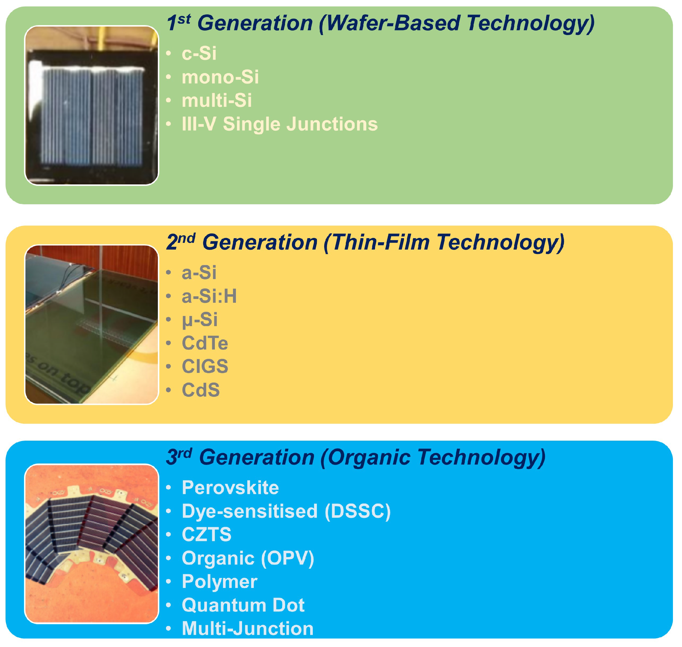
Figure 2.
ABX crystalline structure model.
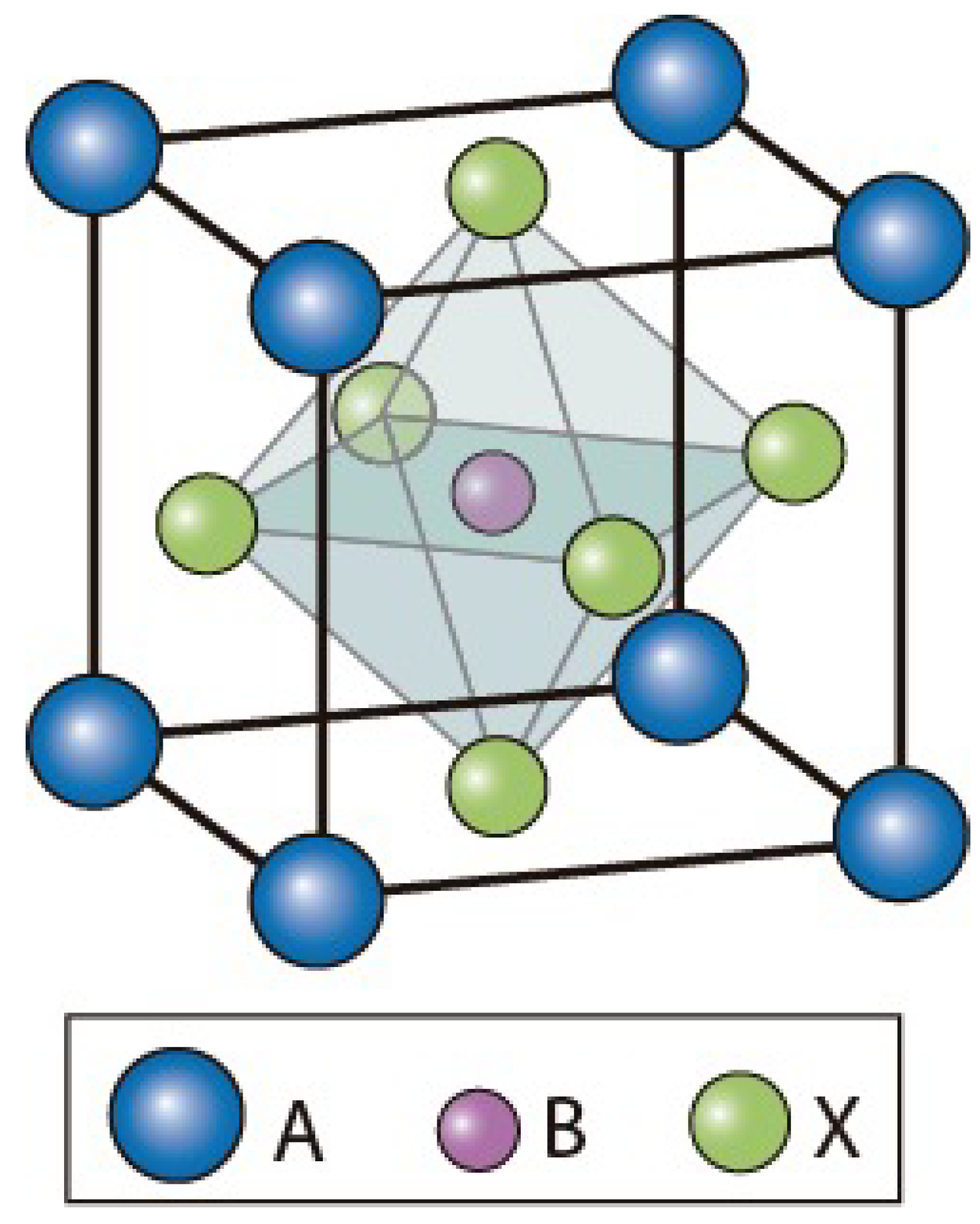
Figure 3.
Diagram of a p-n junction solar cell.
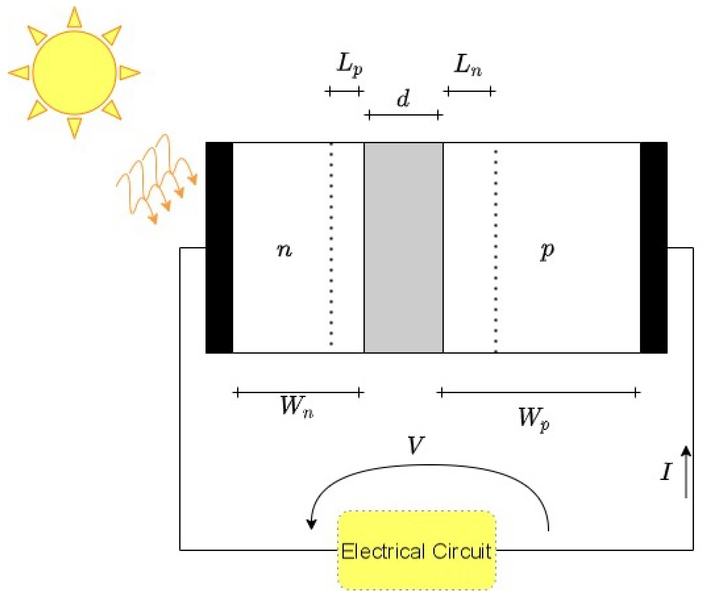
Figure 4.
Electrical equivalent circuit of a solar cell: 1M3P.
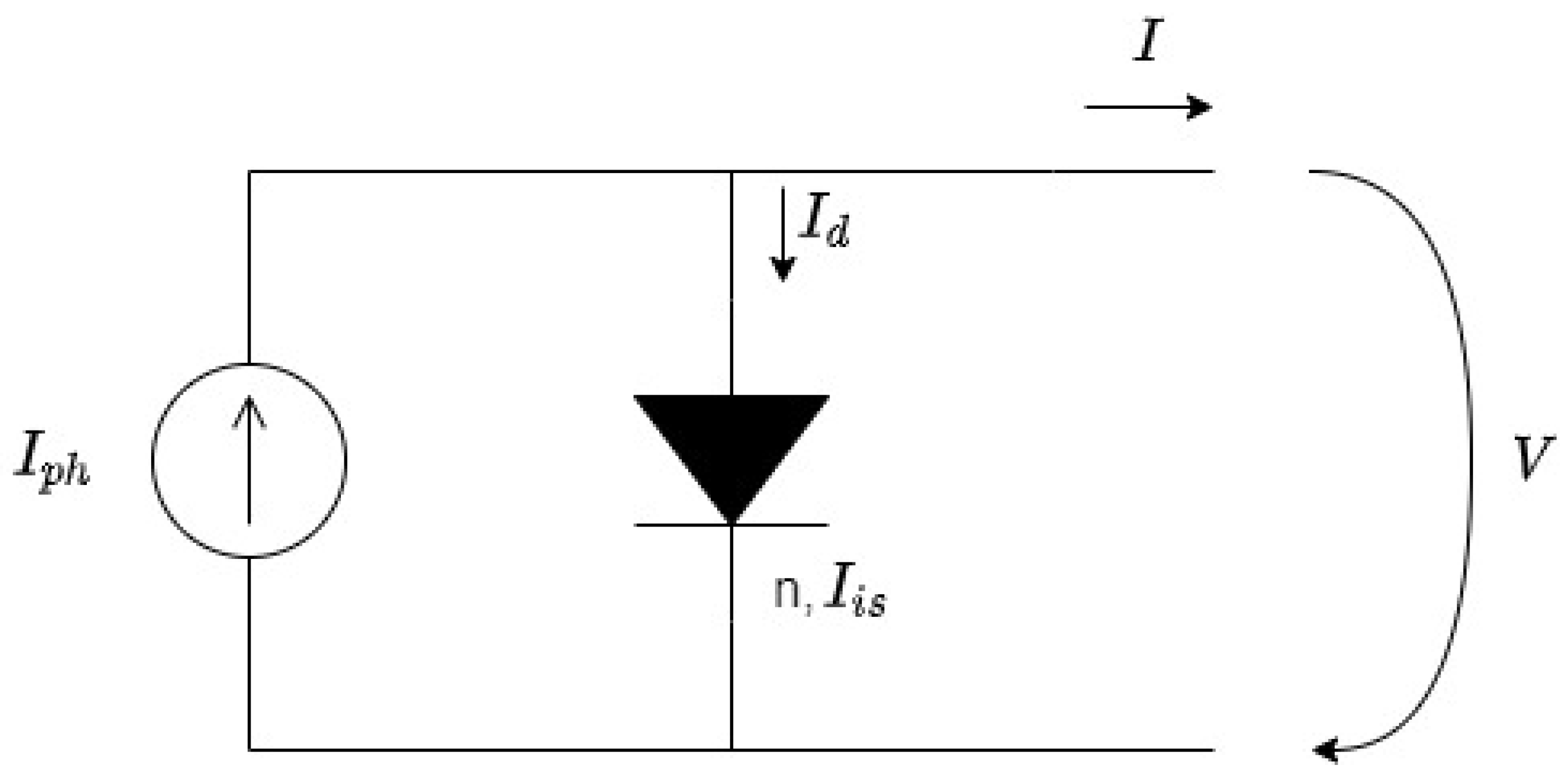
Figure 5.
Example of a I(V) solar cell characteristic (blue) and a graphical solution of its operating point Q for a load resistance R (red).
Figure 5.
Example of a I(V) solar cell characteristic (blue) and a graphical solution of its operating point Q for a load resistance R (red).

Figure 6.
Example of a P(V) solar cell characteristic (blue) and the graphical definition of the maximum power point (red).
Figure 6.
Example of a P(V) solar cell characteristic (blue) and the graphical definition of the maximum power point (red).
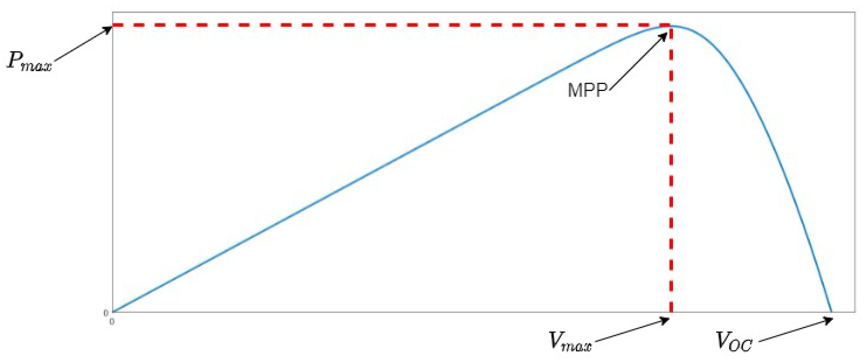
Figure 7.
Electrical equivalent circuit of a solar cell: 1M5P.
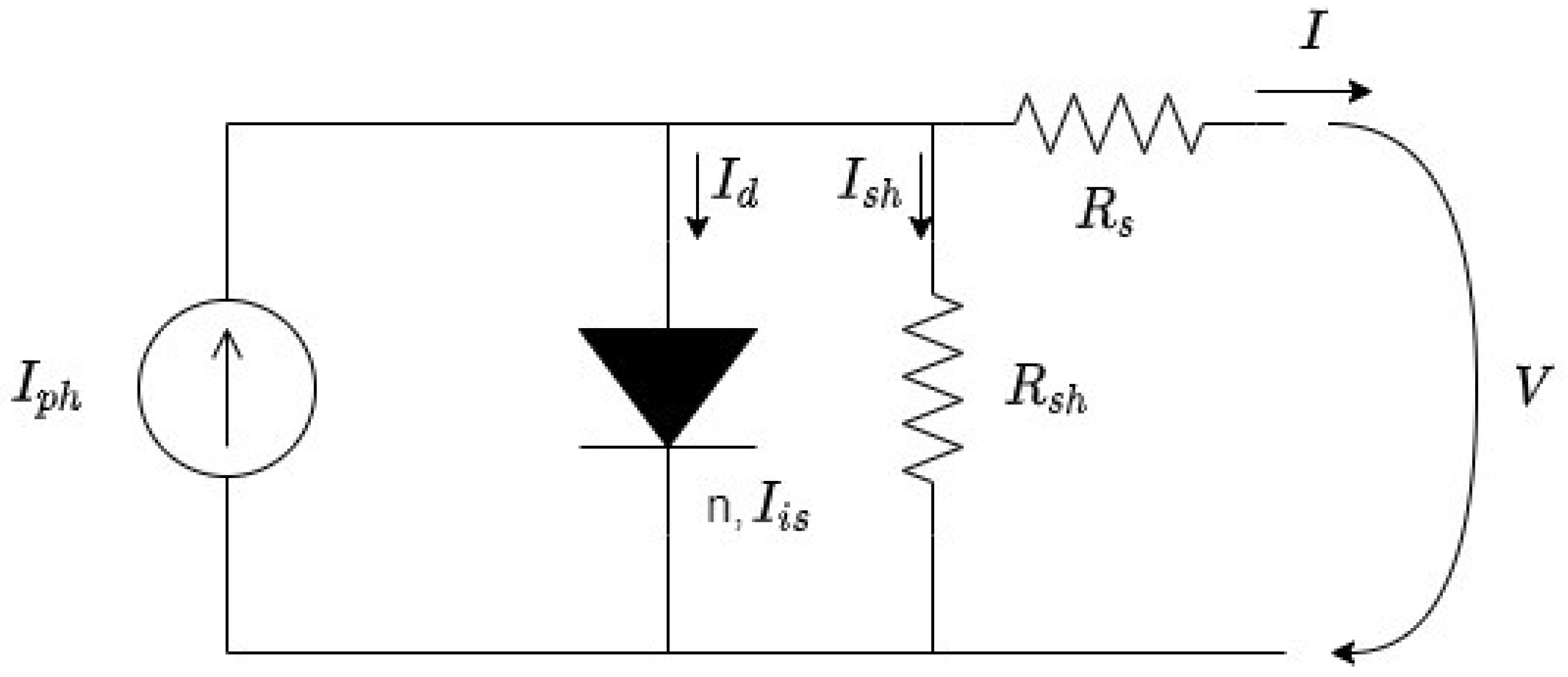
Figure 8.
Example of I(V) curves for different values of : the effect of the shunt resistance on the current–voltage characteristic.
Figure 8.
Example of I(V) curves for different values of : the effect of the shunt resistance on the current–voltage characteristic.
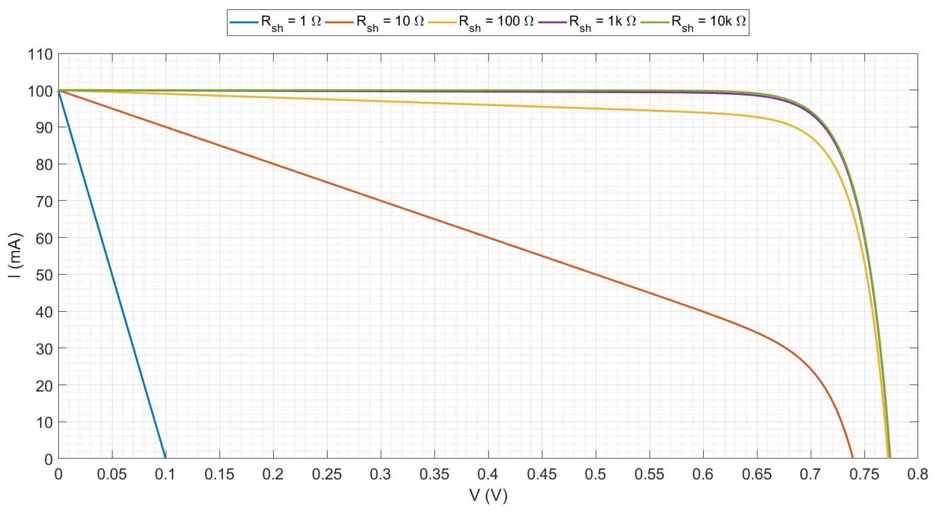
Figure 9.
Example of P(V) curves for different values of : the effect of the shunt resistance on the power–voltage characteristic.
Figure 9.
Example of P(V) curves for different values of : the effect of the shunt resistance on the power–voltage characteristic.
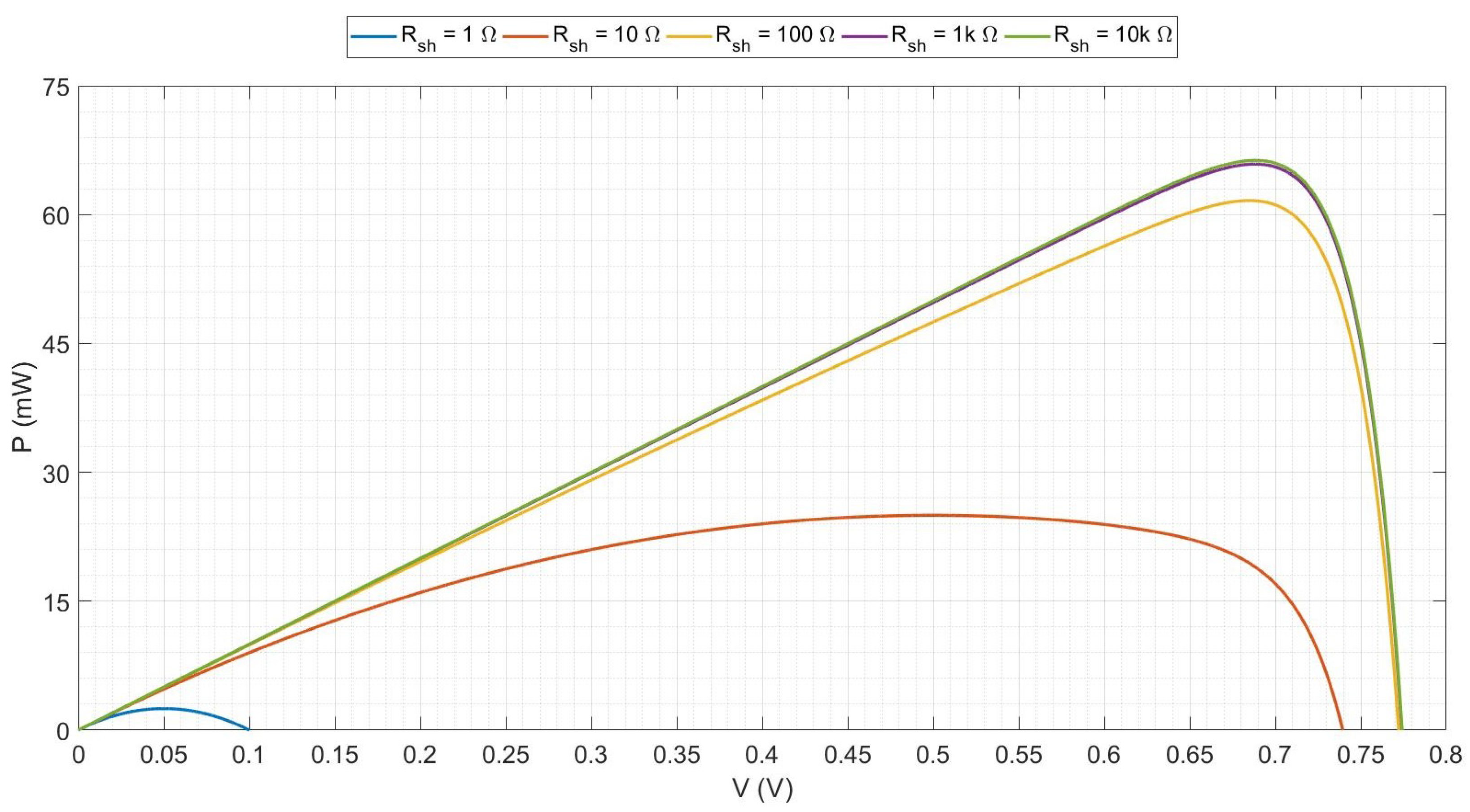
Figure 10.
Example of I(V) curves for different values of : the effect of the series resistance on the current–voltage characteristic.
Figure 10.
Example of I(V) curves for different values of : the effect of the series resistance on the current–voltage characteristic.
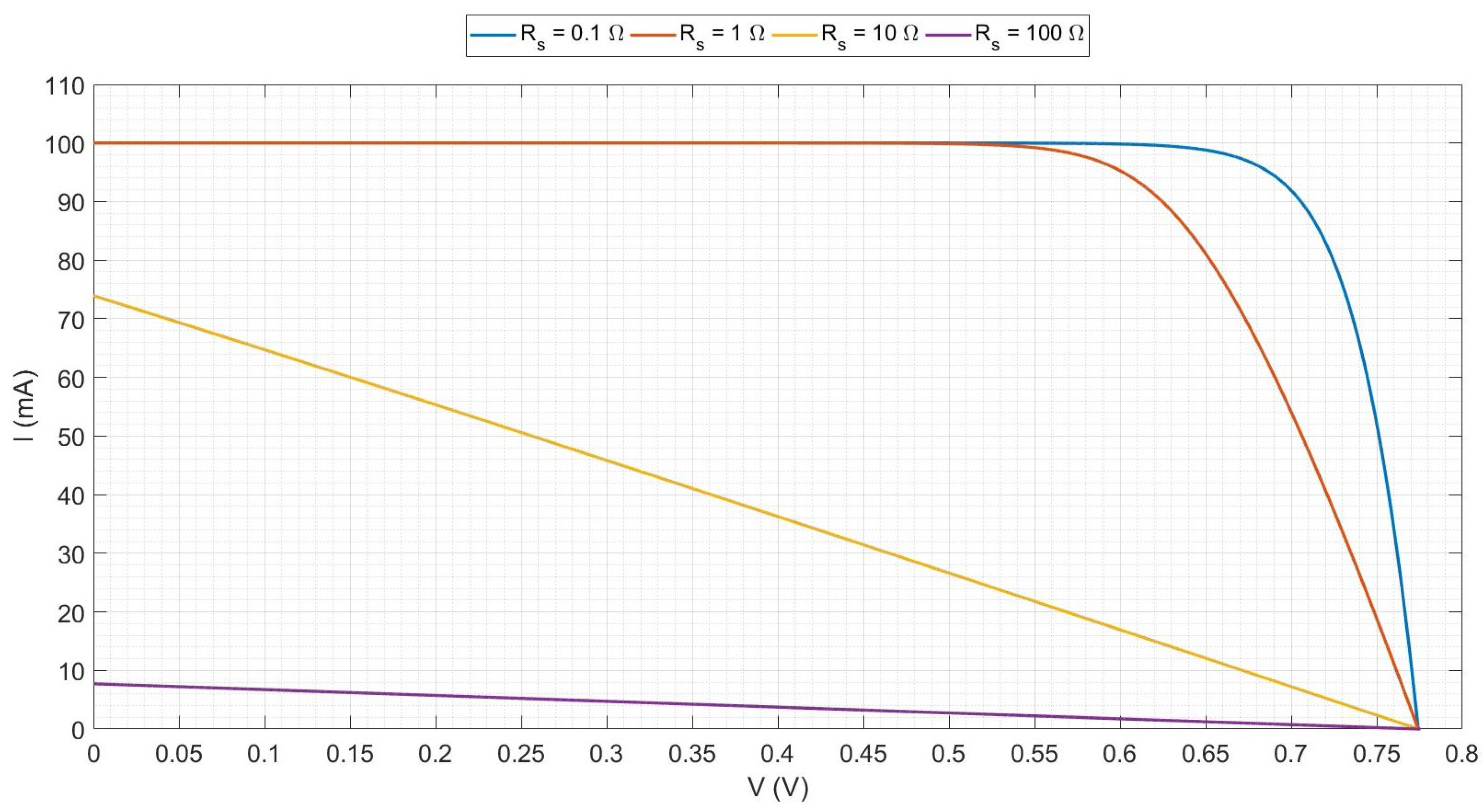
Figure 11.
Example of P(V) curves for different values of : the effect of the series resistance on the power–voltage characteristic.
Figure 11.
Example of P(V) curves for different values of : the effect of the series resistance on the power–voltage characteristic.
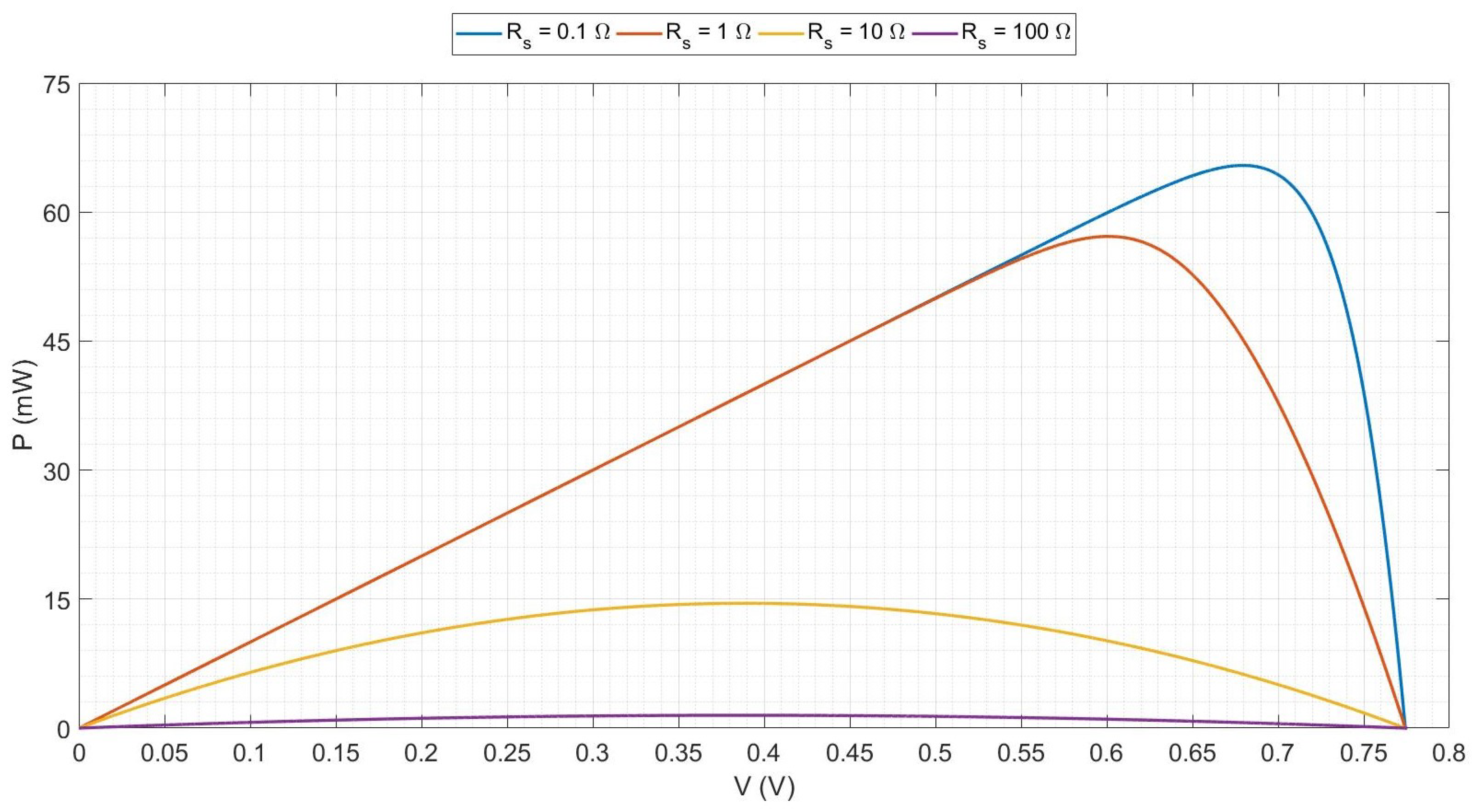
Figure 12.
Example of I(V) curves for different values of : the effect of the series resistance on the current-voltage characteristic.
Figure 12.
Example of I(V) curves for different values of : the effect of the series resistance on the current-voltage characteristic.
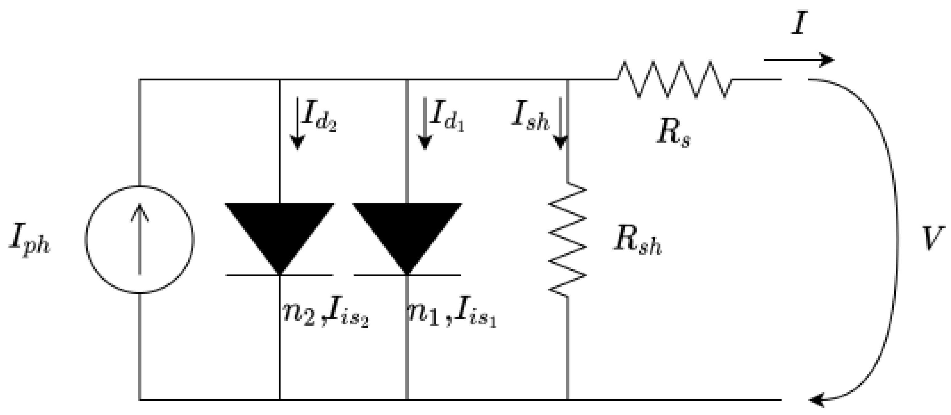
Figure 13.
Distinction about different photovoltaic architectures: from a cell to generators and parks (adapted from [77]).
Figure 13.
Distinction about different photovoltaic architectures: from a cell to generators and parks (adapted from [77]).
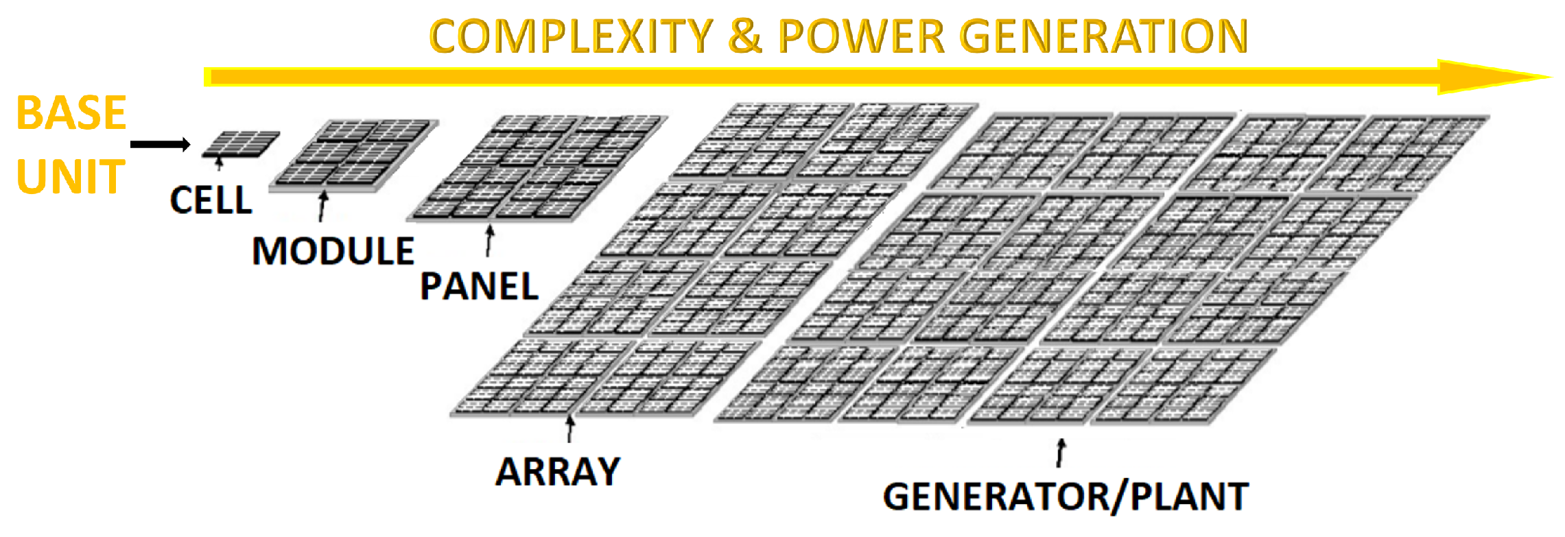
Figure 14.
Different cells associations and modules configurations (adapted from [78]).
Figure 14.
Different cells associations and modules configurations (adapted from [78]).
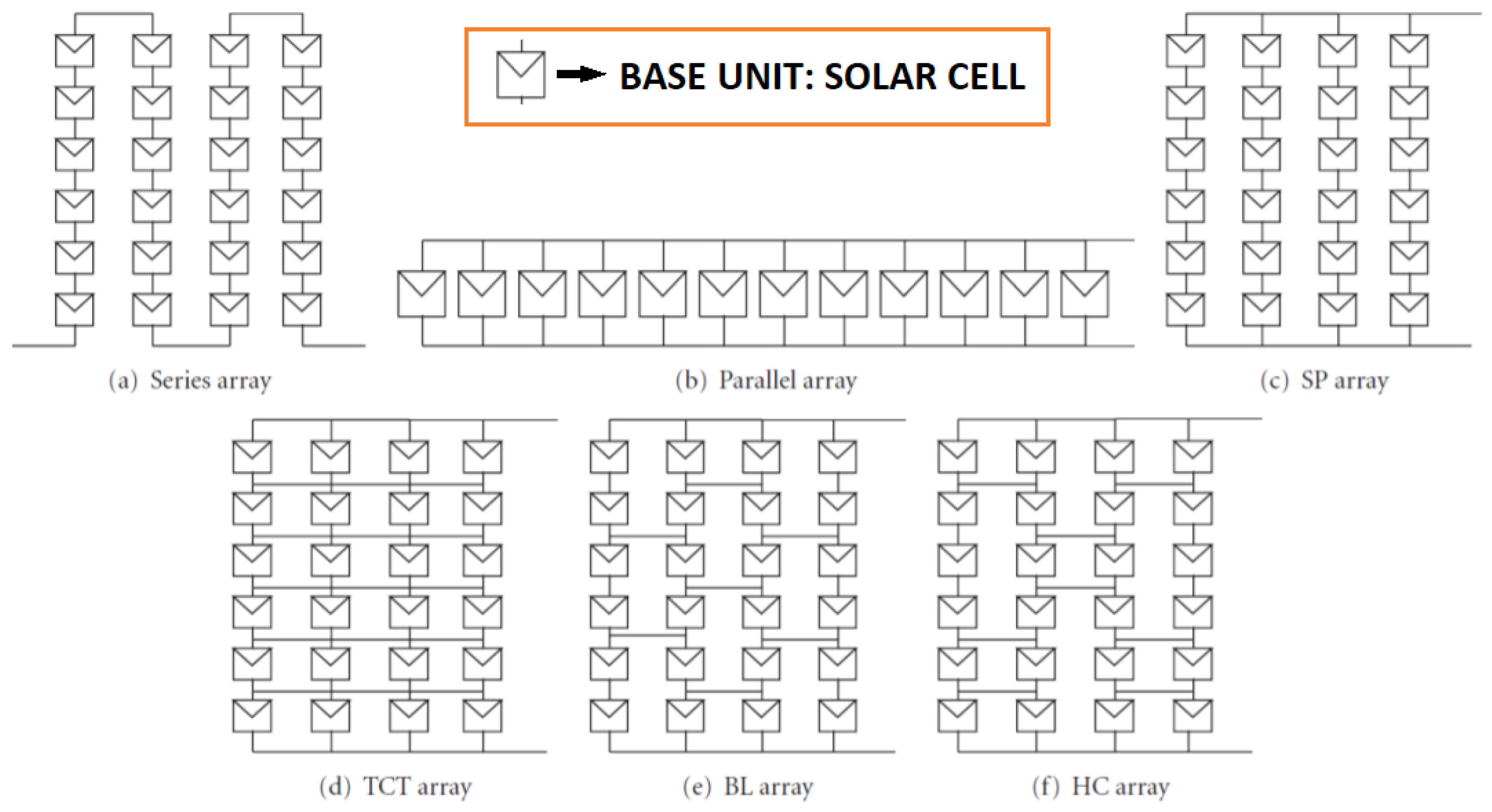
Figure 15.
A schematic of a photovoltaic module.
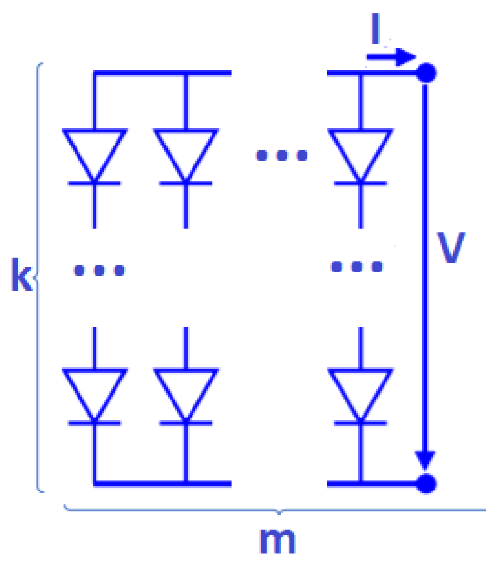
Figure 16.
Solar irradiance spectrum: AM0 and AM1.5 spectral irradiance.
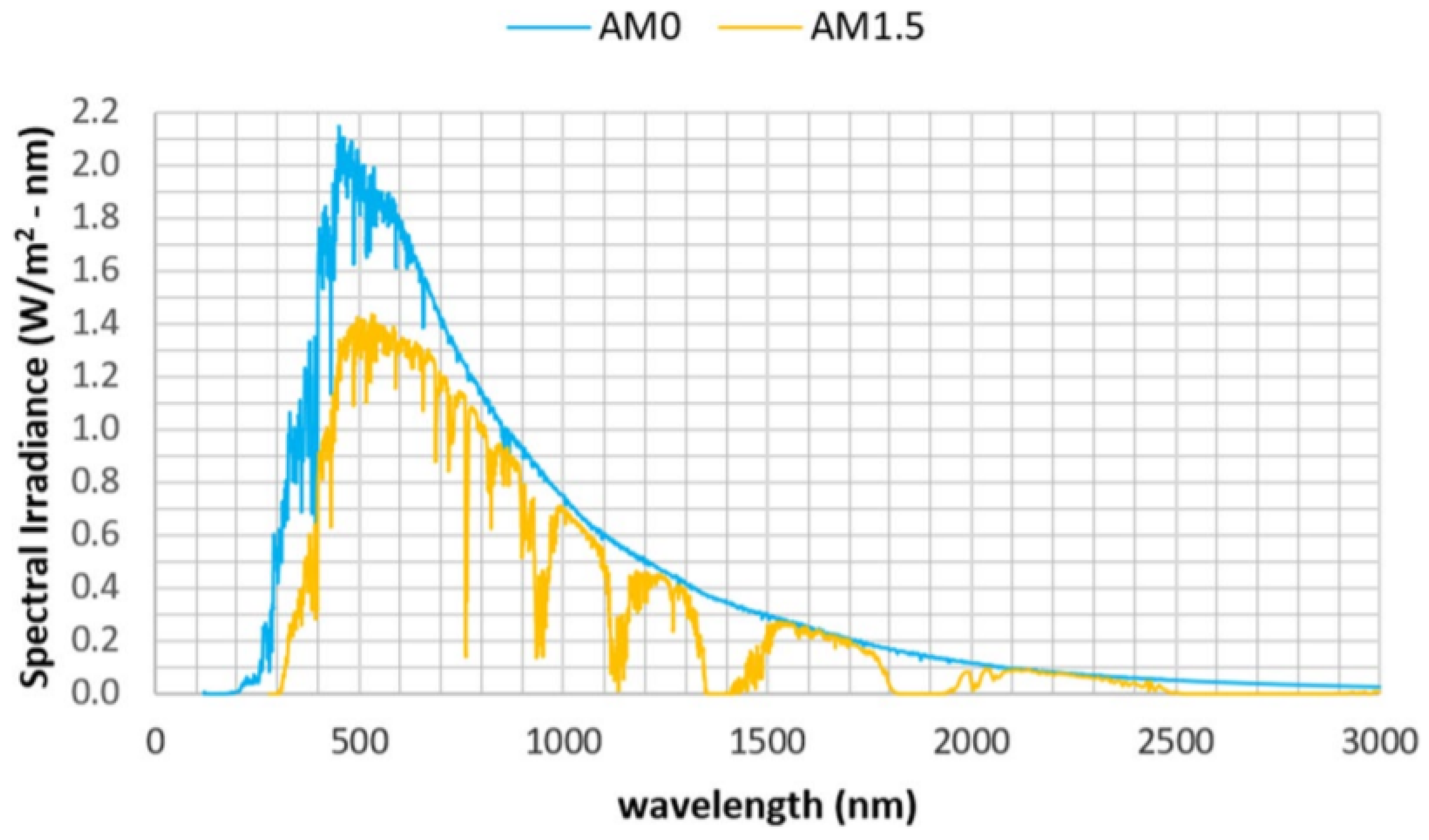
Figure 17.
Main radiation types that may be incident on a photovoltaic solar cell.
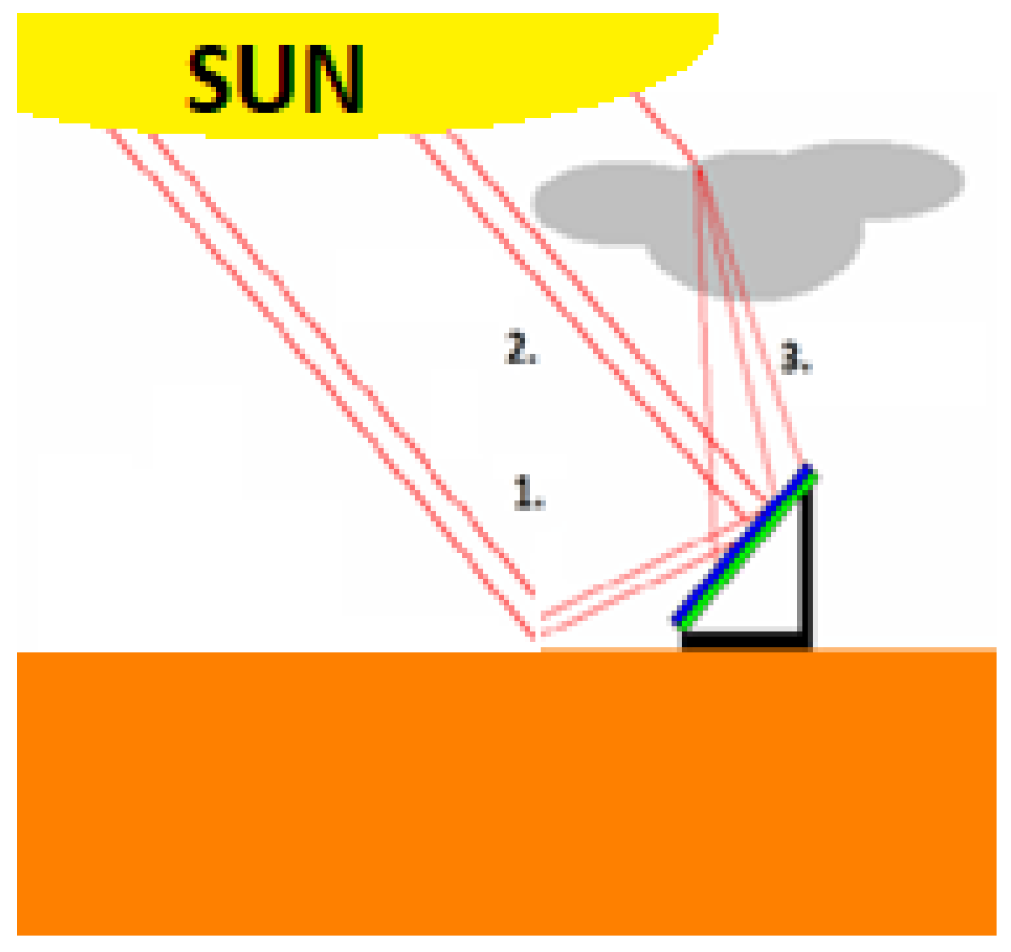
Figure 18.
Schematic of a partially shaded photovoltaic panel.
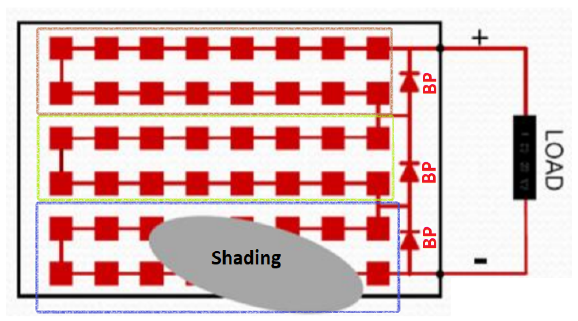
Figure 19.
Example of a usual shading scenario on photovoltaic parks.
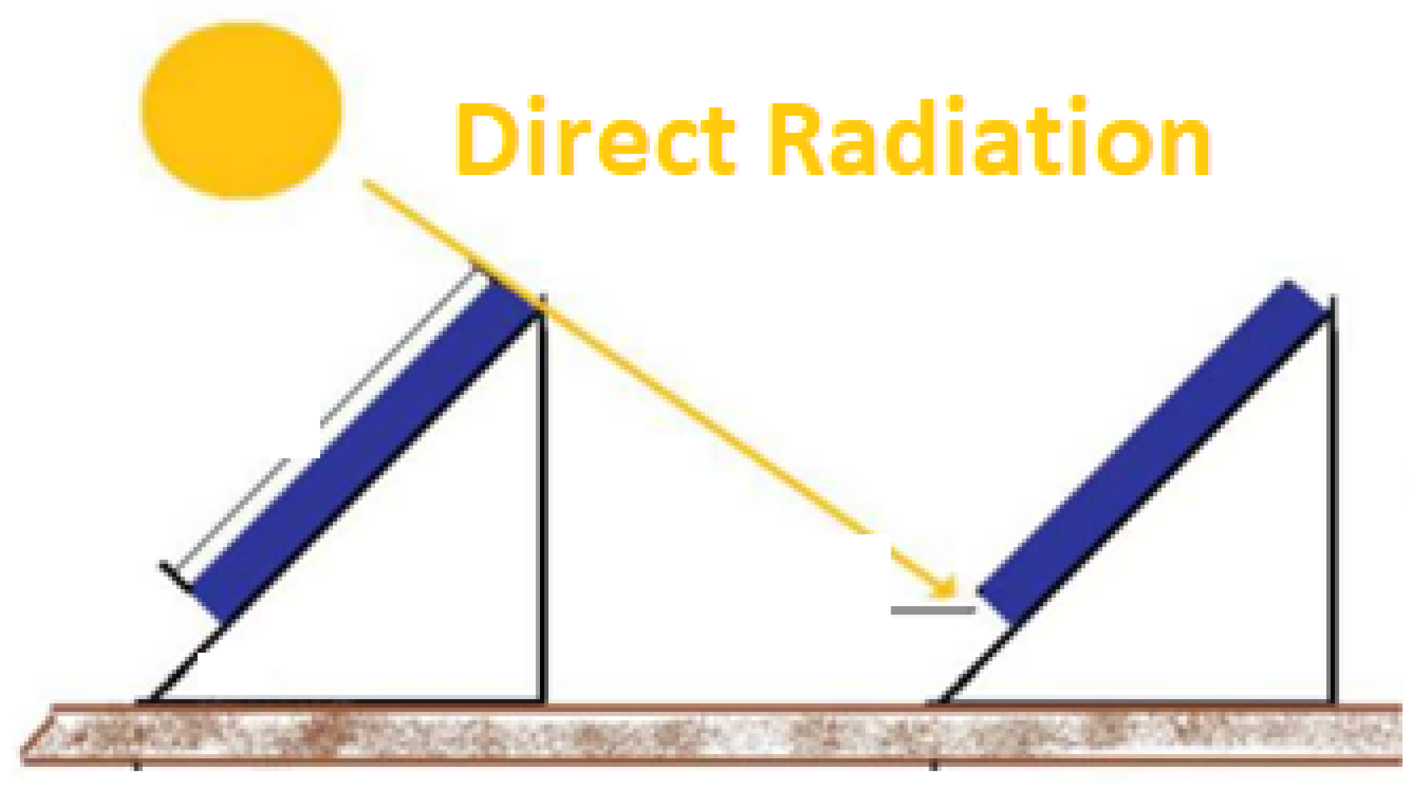
Figure 20.
Typical example of a I(V) characteristic when bypass diodes are active due to different shading levels on a photovoltaic panel.
Figure 20.
Typical example of a I(V) characteristic when bypass diodes are active due to different shading levels on a photovoltaic panel.
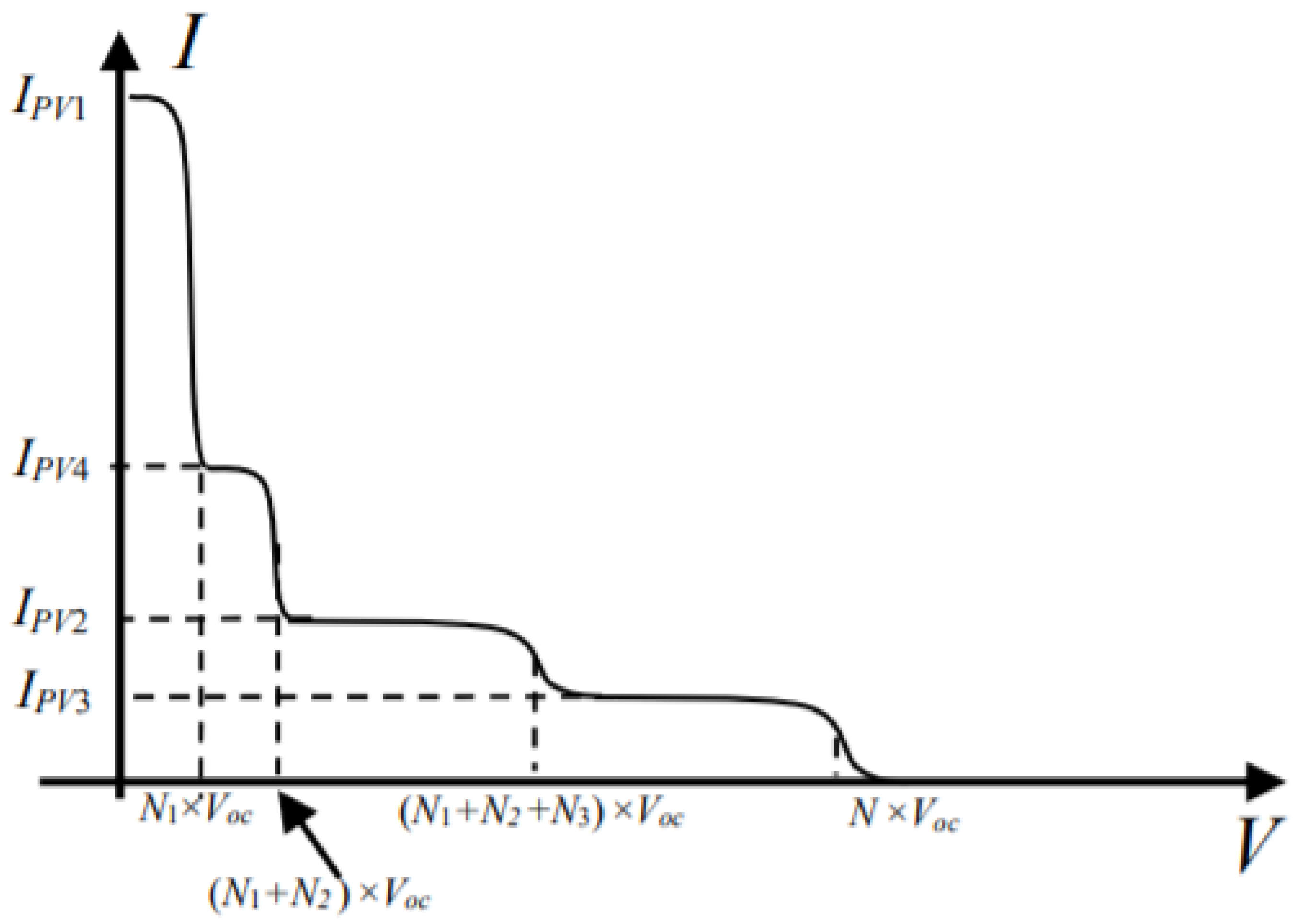

Table 1.
Breakthroughs and research tendencies per cell type technology.
| Multijunction Cells | Cell Type | Top Efficiency [%] | ||
| 3J (concentrator) | 1.385 | 0 | 44.4 | |
| 3J (non-concentrator) | 1.000 | 0.2 | 39.5 | |
| 2J (concentrator) | 0.211 | 0.4 | 35.5 | |
| 2J (non-concentrator) | 0.281 | 0.8 | 32.9 | |
| 4J+ (concentrator) | 0.750 | 0.6 | 47.1 | |
| 4J+ (non-concentrator) | 0.250 | 0.2 | 39.2 | |
| GaAs | Single crystal | 0.182 | 0.4 | 27.8 |
| Concentrator | 0.182 | 0.4 | 30.5 | |
| Thin film crystal | 0.533 | 0.4 | 29.1 | |
| Crystalline Si | Single crystal (concentrator) | 0.088 | 0 | 27.6 |
| Single crystal (non-concentrator) | 0.568 | 0.6 | 26.1 | |
| Multicrystalline | 0.405 | 1.2 | 23.3 | |
| Silicon heterostructures (HIT) | 0.550 | 0.6 | 26.7 | |
| Thin film crystal | 0.450 | 0 | 21.2 | |
| Thin film | CIGS (concentrator) | 0.150 | 0 | 23.3 |
| CIGS | 0.844 | 0.8 | 23.4 | |
| CdTe | 0.533 | 0 | 22.1 | |
| a-Si:H (stabilised) | 0.422 | 0.2 | 14.0 | |
| Emerging | Dye-sensitised | 0.300 | 0.4 | 13.0 |
| Perovskite | 1.500 | 1.6 | 25.5 | |
| Perovskite/Si tandem (monolithic) | 1.500 | 1.2 | 29.5 | |
| Organic | 1.200 | 1.8 | 18.2 | |
| Organic tandem | 0.692 | 0.6 | 14.2 | |
| Inorganic (CZTSSe) | 0.500 | 0.2 | 13.0 | |
| Quantum dot | 1.182 | 1.2 | 18.1 | |
| Perovskite/CIGS tandem | 1.000 | 0.6 | 24.2 |
Table 2.
Advantages and disadvantages of ground mounted, BAPV and BIPV systems.
| Method | Ground Mounted | Building Applied Photovoltaic (BAPV) | Building Integrated Photovoltaic (BIPV) |
|---|---|---|---|
| Advantages | (1) Easy access for repairs and maintenance; (2) Optimizable tilt and orientation; (3) Better airflow. | (1) Easy installation on pre-existing buildings; (2) Well established solution; (3) May offer additional thermal, light, noise and water insulation. | (1) Highly customisable and visually pleasing; (2) May offer additional thermal, noise and light insulation; (3) More secure against theft. |
| Disadvantages | (1) Ground foundations are costly and time consuming to build; (2) Safety issues (accessible to animals and children); (3) Takes up ground space; (4) Very visible. | (1) Easily damaged by strong wind; (2) Installation can damage the building’s structure. | (1) Bound to the surface tilt and orientation; (2) May reach higher temperatures due to poor airflow; (3) Novelty application. |
Table 3.
Methods of integrating photovoltaic systems on buildings.
| Shading | BAPV | (1) Commonly used as louvres that can be fixed or adjustable; (2) Passively limits solar gains; (3) Possible issues with strong wind loads and vibration; (4) Can be placed on external walkways for easy access. |
| Roof Mounted | BAPV | (1) Optimizable tilt and orientation; (2) High visual impact, (3) Require drilling in the structure; (4) Well established. |
| Facade Mounted | BAPV | (1) Might not be approved by the condominium’s assembly; (2) High visual impact; (3) Conditioned orientation and tilt; (4) Structure is bolted into the wall. |
| Rainscreen Cladding | BIPV | (1) Can only be applied on load bearing vertical walls; (2) The air gaps offer space for wiring; (3) Easy to upgrade traditional systems to PV technology; (4) Air gap offers a natural cooling system for PV panels. |
| Curtain Wall Stick System | BIPV | (1) Suitable for low rise buildings due to scaffolding; (2) Easy replacement of modules; (3) Some modules need to be made to measure; (4) Assembled on site. |
| Curtain Wall Unitised System | BIPV | (1) Suitable for low and high rise buildings; (2) Can be installed from inside the buildings (no scaffolding); (3) Wiring is concealed in frame by the manufacturer; (4) All components are made to measure by highly skilled professionals. |
| Double Skin Facade | BIPV | (1) Suitable for see through facades; (2) Offers sound, solar and thermal insulation; (3) Ventilation can be natural or mechanical; (4) Each skin is composed of unitised modules assembled together on site. |
| Atria and Canopies | BIPV | (1) Optimizes floor space usage; (2) Have to be weather-tight; (3) Risk of condensation on the inner side of the panels; (4) Hight heat losses in the Winter and gains in the Summer. |
Publisher’s Note: MDPI stays neutral with regard to jurisdictional claims in published maps and institutional affiliations. |
© 2022 by the authors. Licensee MDPI, Basel, Switzerland. This article is an open access article distributed under the terms and conditions of the Creative Commons Attribution (CC BY) license (https://creativecommons.org/licenses/by/4.0/).
Share and Cite
MDPI and ACS Style
Marques Lameirinhas, R.A.; Torres, J.P.N.; de Melo Cunha, J.P. A Photovoltaic Technology Review: History, Fundamentals and Applications. Energies 2022, 15, 1823. https://doi.org/10.3390/en15051823
AMA Style
Marques Lameirinhas RA, Torres JPN, de Melo Cunha JP. A Photovoltaic Technology Review: History, Fundamentals and Applications. Energies. 2022; 15(5):1823. https://doi.org/10.3390/en15051823
Chicago/Turabian StyleMarques Lameirinhas, Ricardo A., João Paulo N. Torres, and João P. de Melo Cunha. 2022. "A Photovoltaic Technology Review: History, Fundamentals and Applications" Energies 15, no. 5: 1823. https://doi.org/10.3390/en15051823
Note that from the first issue of 2016, this journal uses article numbers instead of page numbers. See further details here.