Abstract
This paper proposes the design of a mixed-mode universal biquad configuration, which realizes generic filter functions in all four possible modes, namely voltage mode (VM), current mode (CM), transadmittance mode (TAM), and transimpedance mode (TIM). The filter architecture employs two voltage differencing buffered amplifiers (VDBAs), two resistors and two capacitors, and can provide lowpass (LP), bandpass (BP), highpass (HP), bandstop (BS), and allpass (AP) biquadratic filtering responses without any circuit alteration. All passive elements used are grounded, except VM. The circuit not only allows for the electronic tuning of the natural angular frequency (ωo), but also achieves orthogonal tunability of the quality factor (Q). It also provides the feature of availability of output voltage at the low-output impedance terminal in VM and TIM, and does not require inverting-type or double-type input signals to realize all the responses. Moreover, in all modes of operation, the high-Q filter can be easily obtained by adjusting a single resistance value. Influences of the VDBA nonidealities and parasitic elements are also discussed in detail. PSPICE simulations with TSMC 0.18-µm CMOS process parameters and experimental testing results with commercially available IC LT1228s have been used to validate the theoretical predictions.
1. Introduction
The design and synthesis of active frequency-selective filters have a very significant role in the areas of continuous-time signal processing, instrumentation and measurement applications, and wireless communication. In recent years, the design of general mixed-mode universal biquadratic filters with input voltages and/or currents and output voltages and/or currents has received a lot of attention from researchers. Considering the nature of input and output signals, the filters can be classified into four possible modes, i.e., voltage mode (VM), current mode (CM), transadmittance mode (TAM), and transimpedance mode (TIM). The VM and CM operations perform frequency filtering behavior on voltage and current signals, respectively. The TAM and TIM operations can be used as bridges for connecting a VM filter to any of the CM circuits and vice versa. Accordingly, the mixed-mode universal filters that provide all generic filtering responses in all four modes increase the versatility and flexibility of practical filtering applications and requirements. Consequently, these filters are worthy of investigation and research. Therefore, in the recent past, several structures realizing mixed-mode universal biquadratic filters with a variety of high-performance active elements have appeared in the literature [1,2,3,4,5,6,7,8,9,10,11,12,13,14,15,16,17,18,19,20,21,22,23,24,25,26,27,28,29,30,31,32,33,34,35,36,37,38,39,40,41,42,43,44,45,46]. Table 1 presents a comparative study of earlier-reported mixed-mode universal filters based on various types of high-performance active components. A deep investigation of the available literature reveals that several exemplary filter topologies introduced in [1,12,16,19,21,26,29,31,32,37,39,43,44] do not provide the different filtering responses in all four modes of operation. In [1,2,3,4,5,6,7,9,10,11,12,13,17,18,20,25,27,28,29,30,32,36,38,40,41], they require more than two active components for the design. The use of more active components results in higher power dissipation and a large chip area. Additionally, a multitude of the previously discussed mixed-mode filters [3,4,5,6,7,8,10,12,16,18,22,23,25,27,31,35,36,38,41,42,44,45] employ an excessive number (at least five) of passive components. It has been observed that the realizations of [3,4,5,6,7,8,12,14,15,16,18,21,22,23,24,26,27,31,33,34,35,37,38,39,41,42,43,45,46] still used some floating passive components, which is unfavorable from integrated circuit (IC) implementation viewpoint. To obtain various filtering responses or to change the operating mode, the designs in [5,7,27,32,42] need structural modification with a programmable switching technique. This technique needs to employ some external switches, which practically lead to increasing switching noise. The filter structures given in [3,4,5,6,7,8,10,12,16,18,22,23,25,31,35,36,38,41] do not provide the feature of inbuilt tunability of filter parameters. Furthermore, the important filter parameters, i.e., natural angular frequency (ωo) and quality factor (Q), for the circuits [1,5,6,7,12,13,15,16,17,19,20,23,30,33,34,37,38,41] are interactive. Although the circuits of [4,13,22,25,27,30,31,32,38] allow the realization of different functions of the universal filter with the same topology, they employ two different types of active components, which are not modular, and increase the complexity of the resulting circuit. In other works [8,16,19,24,26,33,39,43,45,46], some mixed-mode universal filters based on a single active element were previously reported. However, the active devices used for these realizations are complex active components, resulting in a complicated internal structure [8,24,33,39,43,45,46]. Furthermore, the single active element-based filter circuits [16,26,39,43] function only in dual modes of operation. Therefore, it should be concluded that the filter structures presented in [1,2,3,4,5,6,7,8,9,10,11,12,13,14,15,16,17,18,19,20,21,22,23,24,25,26,27,28,29,30,31,32,33,34,35,36,37,38,39,40,41,42,43,44,45,46] suffer from one or more of the following disadvantages: (i) inability to realize various filtering responses in all four possible modes; (ii) use of a greater number of active components; (iii) use of an excessive number of passive components; (iv) use of ungrounded passive elements; (v) need of some external switches; (vi) lack of built-in tuning capability; (vii) inability to control ωo and Q independently; (viii) use of a complex active building block; (ix) need for inverting-type or double-type input signals.

Table 1.
A comparison chart of previously related mixed-mode universal biquad filters.
Due to its simple structure, versatility, and CMOS integrability, the voltage differencing buffered amplifier (VDBA) is an alternative and suitable active building block for biquad filter solutions [47]. Interestingly, the internal circuit architecture of the VDBA block consists of an operational transconductance amplifier (OTA) and a voltage follower (VF) [48,49]. This simple circuitry implementation leads to low power consumption and small chip area requirements. Therefore, in this work we adopt the advantages provided by the VDBA device to design a mixed-mode universal biquad filter. The designed filter topology possesses the following salient properties: (i) use of a reasonable number of active and passive elements (i.e., two VDBAs, two resistors, and two capacitors); (ii) capability of realizing universal biquadratic filter functions in all four modes; (iii) employment of all grounded passive elements, except for VM; (iv) exhibits inbuilt tuning capability; (v) noninteractive control of Q; (vi) low-output impedance for VM and TIM operations. The functionality of the circuit has been evaluated through simulation results based upon TSMC 0.18-µm 1P6M CMOS technology parameters, and furthermore through the experimental measurements of the commercially available integrated circuit (IC), LT1228. Additionally, all properties of the proposed mixed-mode filter are mentioned and compared with the previous related works in Table 1. Furthermore, Table 2 presents a comprehensive comparison illustrating the superiority of the proposed mixed-mode universal filter over the earlier reported relevant VDBA-based biquad configurations [50,51,52,53,54,55,56,57,58]. As can be observed, no earlier VDBA-based filter realization can be operated in all four modes of operation. The passive components used for their realizations are all floating. Although the works proposed in [54,56] use a single VDBA as an active element, they suffer from operating in only a single mode and using at least four floating passive components.
Table 2.
Performance comparison of the proposed filter with the recently proposed VDBA-based biquad filters.
The paper is organized as follows, Section 2 describes the VDBA. The proposed mixed-mode universal filter is proposed in Section 3. The non-ideal gain effect, sensitivity performance, and parasitic impedance effect are investigated in Section 4 and Section 5, respectively. The simulation results are given in Section 6, while the practical circuit implementation and the experimental results are presented in Section 7. Finally, the paper is concluded in Section 8.
2. VDBA Description
The electrical symbol of the VDBA is shown in Figure 1. The defining characteristic of the VDBA can be described by the following matrix equation:
where gm is the transconductance gain of the VDBA. The transconductance gm, as usual, can be tuned by a bias current or voltage, thereby imparting tunability to the structure. Further, α and β are the non-ideal transconductance gain and nonideal voltage gain, respectively. These non-ideal gains can be defined as α = (1 + εα) and β = (1 + εβ), in which the tracking errors are identified as |εα| << 1 and |εβ| << 1. Accordingly, the values of α and β are ideally equal to unity.
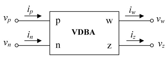
Figure 1.
Electrical symbol of the VDBA.
As mentioned above, the VDBA block comprises two essential circuit blocks: an OTA and a VF [47,48]. The simple CMOS implementation of the VDBA used in this work is shown in Figure 2, in which the OTA consists of transistors M1-M6; and it is followed by a VF formed by transistors M7–M14. A pair of diode-connected PMOS active load (M3–M4) is driven by a source couple pair (M1–M2). The transconductance gain (gm) of the OTA stage can be externally tuned by the bias current (IB), as described by the following expression:
where Kn = μnCox is the transconductance parameter, and (W/L) is the ratio of the width-to-length of the transistors M1 and M2. Note from Equation (2) that the transconductance gm is electronically adjustable utilizing IB.
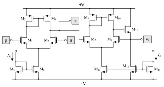
Figure 2.
Possible CMOS realization of the VDBA.
Further, the voltage drop across the grounded impedance at terminal z (vz) is then conveyed to the w terminal with a unity voltage gain by the VF. Thus, the negative-feedback loop established by M7-M11 provides a very low output impedance at the w terminal. For the simulation purpose, the TSMC 0.18-µm level 7 CMOS model parameter has been employed, where the transistor aspect ratios are given in Table 3.
Table 3.
Transistors’ aspect ratios in Figure 2.
3. Proposed Mixed-Mode Universal Biquad Filter
The proposed configuration, which is realized by two VDBAs, two resistors, and two capacitors, is shown in Figure 3. It is important to note that, in this realization, the resistors R1 and R2 are permanently grounded. From the proposed circuit in Figure 3, the universal biquadratic filter operated in all four possible modes is available as follows.
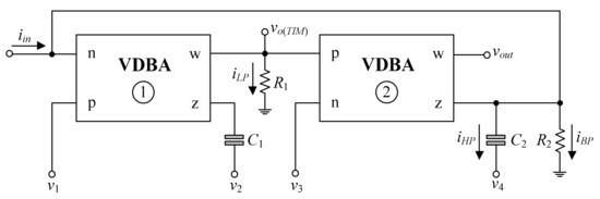
Figure 3.
Proposed mixed-mode biquadratic filter using VDBAs.
- ⮚
- For VM operation: Assuming ideal VDBA (i.e., α =β = 1) and setting iin = 0, the general voltage biquadratic transfer functions of this MISO filter can be obtained as follows.
- With vin = v1 (input voltage) and v2 = v3 = v4 = 0 (grounded), then the LP response is realized as:
- With vin = v2, v1 = v3 = v4 = 0, and gm2 = 1/R2, then the BP response is realized as:
- With vin = v4, and v1 = v2 = v3 = 0, then the HP response is realized as:
- With vin = v1 = v4, and v2 = v3 = 0, then the BS response is realized as:
- With vin = v1 = v3 = v4, v2 = 0, and gm2 = 1/R2, then the AP response is realized as:whereUnder appropriate conditions, the proposed circuit realizes all five generic biquadratic filter responses at vout, which are taken from the w-terminal of VDBA2. Thus, the voltage output of the circuit has a very low output impedance, which is suitable for VM cascadability. Moreover, in this MISO configuration, there is no requirement for negative and double input voltage signals to realize the desired filter responses.
- ⮚
- For CM operation: If v1 = v2 = v3 = v4 = 0 (grounded), the CM biquad transfer functions for this SIMO filter, attained from the circuit analysis of Figure 3, are given byandwhere H0 is the passband gain equal to 1/gm2R1. Additionally, for R1 = 1/gm2, the BS current response can be realized by connecting the appropriate output currents as iBS = iHP – iLP. In the same way, the AP response can also be obtained by the interconnection of LP, BP, and HP responses as iAP = iHP – iBP – iLP.
- ⮚
- For TAM operation: With vin = v3 and v1 = v2 = v4 = 0, then we obtain the TAM filter functions as follows:andEquations (12)–(16) represent the TAM filter functions of the LP, BP, HP, BS, and AP responses with controllable passband gains, respectively. Gain constants can be defined as H1 = 1/R1 and H2 = gm2. It should also be noted from Equations (15) and (16) that a simple component matching condition (R1 = 1/gm2) is required in the case of BS and AP filter realizations.
- ⮚
- For TIM operation: With all input voltages kept grounded (v1 = v2 = v3 = v4 = 0), the configuration in Figure 3 now works in TIM. For this operation, the circuit will realize only two LP and BP biquad filter functions without the requirement of any component matching constraints. The TIM transfer functions related to the outputs vout and vo(TIM) of the circuit are given byandwhere H3 = R2.
In all the above working modes, the important filter characteristics ωo and Q according to Equation (8) are found as:
and
Inspection of Equations (19) and (20) reveals that the characteristic frequency ωo can be tuned electronically through the transconductance gmi (i = 1, 2) of the corresponding VDBA. Moreover, the filter parameter Q is independently controllable by the R2. Hence, the high-Q filter could be conveniently obtained by simply adjusting a single resistance R2.
4. Analysis of the Non-Ideal Gain Effect and Sensitivity Performance
Considering only the influence of the non-ideal gains (α =β ≠ 1), the characteristics ωo and Q of the proposed filter will be modified as:
and
where αi and βi (i = 1, 2) are the parameters α and β of the i-th VDBA, respectively.
The sensitivity analysis of ωo and Q with respect to active and passive components is also carried out, and the calculation results are obtained as:
and
It can be easily deduced that all the sensitivity coefficients of ωo and Q are not greater than one in all four modes of operation.
5. Analysis of the Parasitic Impedance Effect
In this section, the effect of various parasitic impedances of the employed VDBA on the performance of the proposed mixed-mode universal filter in Figure 3 is to be analyzed. In practice, the non-ideal VDBA model with its various terminal parasitics is represented in Figure 4. It appears that the finite parasitic resistances and capacitances at the p, n, and z terminals are in the form [Rp//(1/sCp)], [Rn//(1/sCn)], and [Rz//(1/sCz)], respectively, while the low-value serial resistance (Rw) appears at the w terminal. Ideally, these parasitic values are assumed to be Rp = Rn = Rz = ∞, Rw = 0, and Cp = Cn = Cz = 0. Under the effect of these parasitics, the non-ideal denominator of all transfer functions in all four working modes becomes:
where R′2 = R2 // Rz2 // Rn1, C′1 = C1 + Cz1, and C′2 = C2 + Cz2 + Cn1. Equation (27) illustrates that the order of the filter function is modified due to the parasitic pole ωparasite, (i.e., ωparasite = 1/Rw1Cp2). However, this effect can be diminished if the proposed circuit is designed to operate at a useful frequency much less than ωparasite or under the following condition: ω << 0.1 ωparasite. As the term (sRw1Cp2 + 1) is made close to unity, Equation (27) can be further simplified to
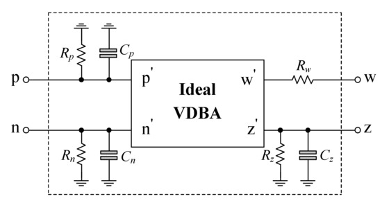
Figure 4.
Non-ideal equivalent circuit of the VDBA.
From Dn(s), the expressions for ωo and Q in the presence of parasitic impedances are thus obtained as:
and
Therefore, it may be concluded that the parasitic effects on the ωo and Q would be alleviated if the following designs must be satisfied:
and
maximum (R1, R2) << parasitic resistances (Rn1, Rp2, Rz2),
minimum (C1, C2) >> parasitic capacitances (Cn1, Cz1, Cz2).
6. Simulation Results
The functionality of the proposed mixed-mode universal filter in Figure 3 was validated by the PSPICE circuit simulation program. The VDBA was modeled using the CMOS structure mentioned in Figure 2 with ±V = 0.75 V and IA = 15 µA. In all simulations, the capacitor values were chosen with C1 = C2 = 50 pF. The circuit was designed for fo = ωo/2π = 1.52 MHz and Q = 1; the active and passive components were chosen as: gm1 = gm2 = 0.48 mA/V (IB1 = IB2 = 50 µA), and R1 = R2 = 2 kΩ. Figure 5 and Figure 6 illustrate the ideal and simulated LP, BP, HP, BS, and AP frequency responses for VM and TAM (i.e., when the input is voltage), respectively. Figure 7 shows the ideal and simulated LP, BP, and HP gain responses for CM and LP and BP in TIM (i.e., when the input is current). The simulated fo of the BP filter was measured as 1.44 MHz, which is an error of 5.26% concerning its theoretical value. The simulation results of Figure 6 also show that the passband gain H1 of the LP response for TAM is obtained as −66 dBS, which depends on H1 = 20 log10 (1/R1). Similarly, the passband gains H2 for BP, HP, BS, and AP responses are the same as the gain H1 of the LP filter because of H2 = 20 log10 (gm2) due to gm2 = 1/R1.
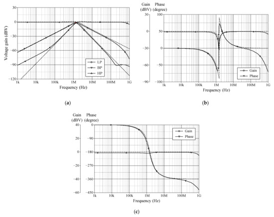
Figure 5.
Ideal (dashed line) and simulated (solid line) frequency responses for VM: (a) LP, BP and HP; (b) BS; (c) AP.
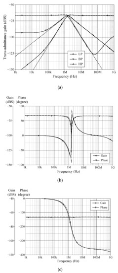
Figure 6.
Ideal (dashed line) and simulated (solid line) frequency responses for TAM: (a) LP, BP and HP; (b) BS; (c) AP.
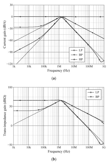
Figure 7.
Ideal (dashed line) and simulated (solid line) frequency responses for CM and TIM: (a) LP, BP, HP in CM; (b) LP and BP in TIM.
To examine the transient behavior of the proposed filter, the LP, BP, and HP responses were carried out for the VM operation. The sinusoidal input voltage of 50 mV (peak) at a frequency of 1.52 MHz was applied and the corresponding output current waveforms are given in Figure 8. As can be monitored, the phase differences between the input and LP, BP, and HP outputs are found to be −92.73°, 5.45°, and 87.29°, which are consistent with ideal values equal to −90° 0°, and 90°, respectively. The percentages of the total harmonic distortion (THD) for the three filter outputs are 0.22% for LP, 1.12% for BP, and 0.64% for HP. In addition, the THD variations of the LP, BP, and HP output voltages on the input signal amplitudes are also shown in Figure 9. It is shown that when the applied input signal amplitude increases by 100 mV (peak), the THD values are within 2.2%. Through the simulation results, the circuit has a total power consumption of 0.373 mW.
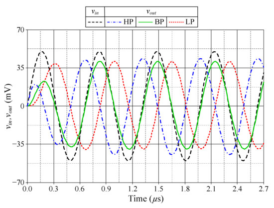
Figure 8.
Transient analysis responses of the proposed filter in VM.
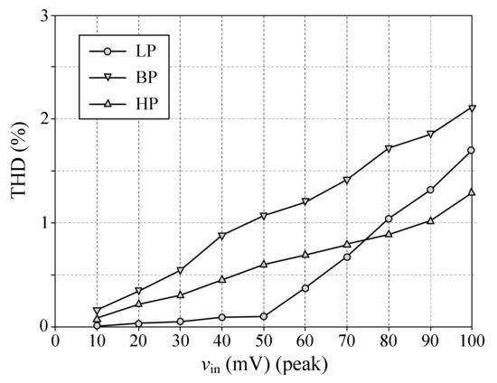
Figure 9.
THD variations of the LP, BP, and HP output waveforms in VM.
As indicated in Equations (19) and (20), the parameters ωo and Q of the proposed filter can be set orthogonally. Figure 10 shows the Q-factor adjustability of the BP responses in VM for various values of R2. In this case, the Q-factors are set as 0.5, 2.4, 9.5, and 95.5 with the R2 value of 1 kΩ, 5 kΩ, 20 kΩ, and 200 kΩ, respectively. The results demonstrate that the high-Q tuning can be achieved by adjusting R2 without influencing fo. Figure 11 represents the VM gain responses of the BP filter for three different values of IB and R2. The BP filter is designed for fo = 1.12 MHz, 2.15 MHz, and 3.72 MHz, while keeping Q fixed at 9.5. Table 4 gives the component values used in Figure 11 and the corresponding calculated and simulated fo.
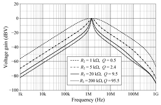
Figure 10.
Simulated BP gain responses in VM for variation in Q with fo = 1.52 MHz.
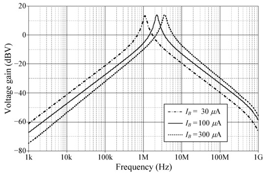
Figure 11.
Simulated BP gain responses in VM for variation in fo with Q = 9.5.
Table 4.
Details of component settings used to obtain a specified fo in Figure 11.
To study the effect of temperature variations, the proposed filter was analyzed under various ambient temperatures. Figure 12 demonstrates the simulated frequency responses of the AP filter in VM for different temperatures (0 °C, 20 °C, 50 °C, 75 °C, and 100 °C). At the natural angular frequency fo = 1.52 MHz, the simulation results show that the gain and phase responses lie within the range of –1.3 dBV to –2.7 dBV, and –184° to –228°, respectively. This variation does not have a strong effect on the gain and phase responses of the circuit. The noise behavior of the proposed filter versus the frequency has also been evaluated, as shown in Figure 13. The output voltage noises of the BP filter at the frequency of 1.52 MHz were found to be 20.50 nV/Hz1/2 for VM and TIM operations, while the output current noises for CM and TAM were 8.45 pA/Hz1/2.
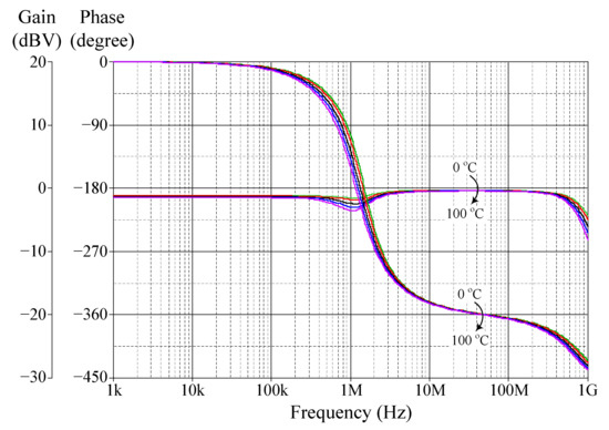
Figure 12.
Simulated AP frequency responses for various temperatures (0 °C, 20 °C, 50 °C, 75 °C and 100 °C).
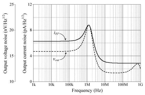
Figure 13.
Output voltage and current noises for the BP filters in VM, TIM and CM, TAM.
The Monte Carlo statistical analysis of the proposed filter is next performed to perceive the effects of the passive component deviations on the filter performance. Statistical analysis with 5% random deviation in both resistor and capacitor values was performed simultaneously for 200 samples. The results for LP, BP, and HP responses in VM operation are achieved as in Figure 14. Additionally, the corresponding histogram demonstrating the fo variations in BP output is shown in Figure 15. According to the statistical results, the mean, median, and standard deviation were, respectively 1.50134 MHz, 1.49936 MHz, and 53.2151 kHz, which implies that the proposed filter exhibits a reasonable sensitivity figure to the passive component tolerances. This further validates the robustness of the design.
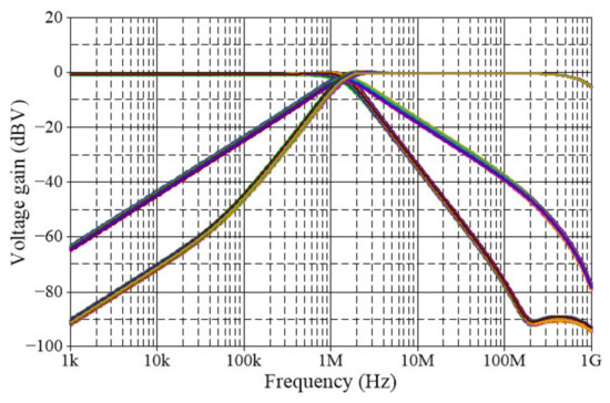
Figure 14.
Monte Carlo statistical analysis results for LP, BP, and HP responses in VM.
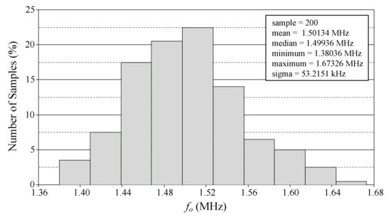
Figure 15.
Histogram of fo distribution of the BP filter in VM.
7. Experimental Results
The features of the proposed mixed-mode universal filter configuration in Figure 3 were also verified by laboratory experiments using a commercially available IC LT1228 from Linear Technology [59]. Figure 16 shows the PCB realized for measurement purposes. The supply voltage used was ±5 V. The experimental setup of the proposed mixed-mode universal filter utilizing the PCB board in Figure 16 is also shown in Figure 17. In CM and TIM measurements, an additional AD844 and a conversion resistor RC were employed to perform the voltage-to-current conversion (V-to-I), where RC = 1 kΩ. On the other hand, to obtain CM and TAM filter results, two AD844s and a resistor RC were employed as a current-to-voltage converter (I-to-V). The passive and active components were selected as R1 = R2 = 1 kΩ, C1 = C2 = 100 pF, and gm1 = gm2 = 1 mA/V (IB1 = IB2 = 100 µA, where gmi = 10 IBi). As a consequence, the theoretical filter parameters for this design were fo = 1.59 MHz and Q = 1. Figure 18 shows the experimental measurements in the time domain of the input and output responses in VM operation, for a 50 mV (peak) sinusoidal input voltage (vin) at 1.59 MHz. The corresponding spectral analyses of the vout were also measured, and the results are provided in Figure 19. The measured results indicate that the THD figures for the LP, BP, HP, BS, and AP output responses were found to be 1.23%, 2.05%, 1.78%, 0.87%, and 2.04%, respectively. Hence, they have no significant distortion that can be observed in our frequency range of interest. The experimental results of Figure 19 also show that the spurious-free dynamic range (SFDR) for the cases of LP, BP, HP, BS, and AP were determined to be 40.70 dBc, 34.60 dBc, 38.07 dBc, 44.82 dBc, and 34.66 dBc, respectively.
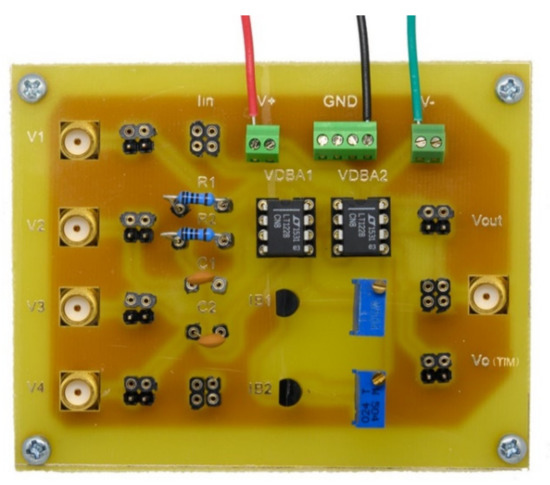
Figure 16.
PCB of Figure 3 used for experimental verification.
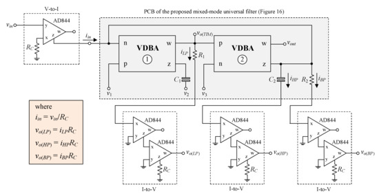
Figure 17.
Experimental setup for measuring the CM, TAM, and TIM filter results.
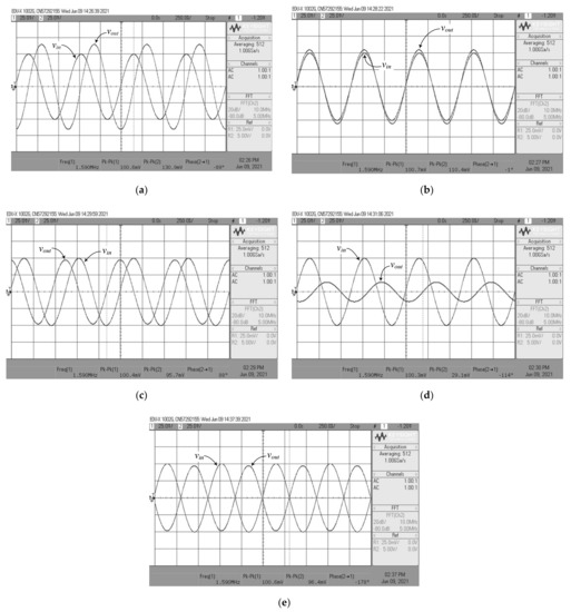
Figure 18.
Measured time-domain waveforms of the proposed VM filter: (a) LP; (b) BP; (c) HP; (d) BS; (e) AP.
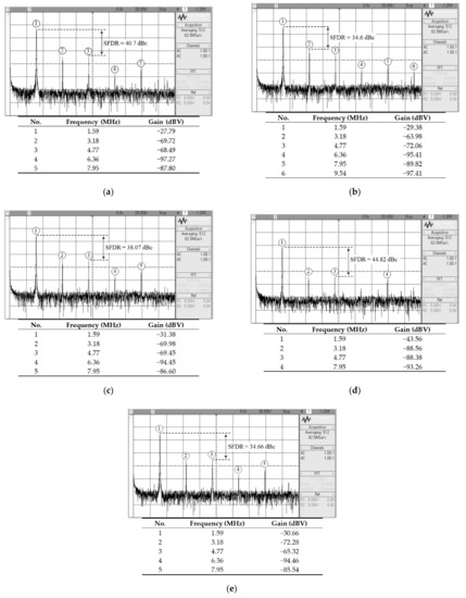
Figure 19.
Measured frequency spectrum of vout of the proposed VM filter: (a) LP; (b) BP; (c) HP; (d) BS; (e) AP.
Furthermore, the ideal and experimental results of the frequency-domain responses obtained from the VM, CM, TAM, and TIM filters are given in Figure 20, Figure 21, Figure 22 and Figure 23, respectively. The results of Figure 20, Figure 21, Figure 22 and Figure 23 show that a good agreement between experimental measurements and theoretical predictions can be observed, as desired. Additionally, the experimental THD variations of the BP output in all modes of operation are plotted for various input signal amplitudes at f = 1.59 MHz, as given in Figure 24.
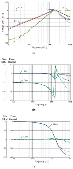
Figure 20.
Ideal (dashed line) and measured (solid line) frequency responses for VM: (a) LP, BP and HP; (b) BS; (c) AP.
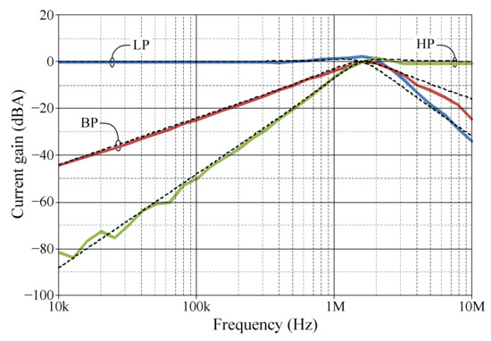
Figure 21.
Ideal (dashed line) and measured (solid line) frequency responses for CM.
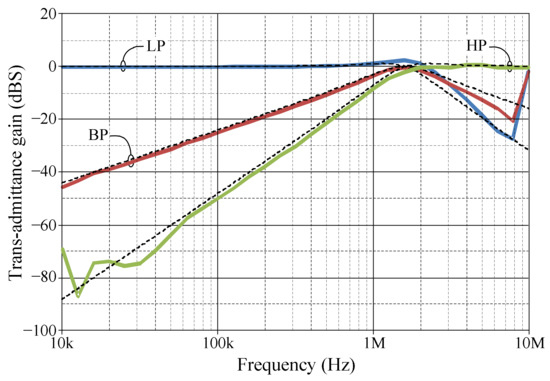
Figure 22.
Ideal (dashed line) and measured (solid line) frequency responses for TAM.
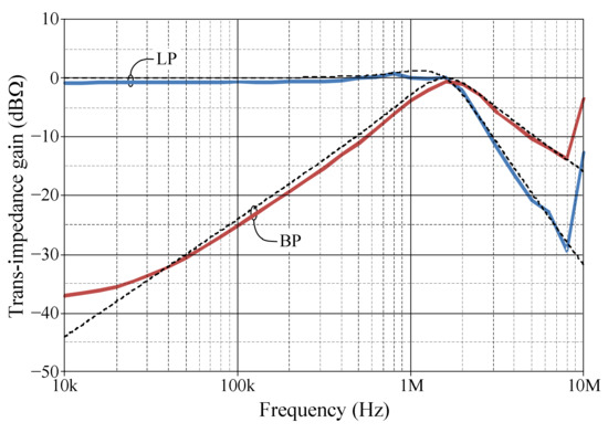
Figure 23.
Ideal (dashed line) and measured (solid line) frequency responses for TIM.
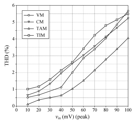
Figure 24.
Measured THD values of the BP outputs for various sinusoidal input signals at a frequency of 1.59 MHz.
8. Conclusions
In this work, a mixed-mode universal filter configuration has been proposed based on only two VDBAs, two grounded resistors, and two capacitors. The proposed circuit is capable of realizing all five biquadratic filtering functions in VM, CM, and TAM operation. In TIM operation, the circuit can realize LP and BP responses. The circuit satisfies the major advantages simultaneously such as (i) employment of grounded passive components, except for VM operation; (ii) having electronic tunability for ωo; (iii) independent controllability of its quality factor; (iv) unemploying inverting-type or double-type input signals; (v) having low output impedance for VM and TIM operations; (vi) low active and passive sensitivity features. The high-Q filter can be easily achieved through a single resistance adjustment. The mathematical analyses such as non-ideal gains, sensitivity performance and parasitic analysis along with the numerical simulation results and experimental measurement results are shown, in order to strengthen the design idea.
Author Contributions
Conceptualization, N.R. and W.T.; methodology, N.R. and W.T.; software, N.R. and M.F.; validation, N.H. and W.T.; formal analysis, M.F.; investigation, N.R., M.F., N.H. and W.T.; resources, N.R. and W.T.; data curation, N.R. and W.T.; writing—original draft preparation, N.H. and W.T.; writing—review and editing, N.H. and W.T.; visualization, N.R. and W.T.; supervision, W.T.; project administration, W.T.; funding acquisition, N.R., M.F., N.H. and W.T. All authors have read and agreed to the published version of the manuscript.
Funding
This research received no external funding.
Institutional Review Board Statement
Not applicable.
Informed Consent Statement
Not applicable.
Data Availability Statement
The data supporting the results presented in this work are available on request from the authors.
Acknowledgments
This work was supported by King Mongkut’s Institute of Technology Ladkrabang (KMITL).
Conflicts of Interest
The authors declare no conflict of interest.
Symbols
The following symbols are used in this manuscript:
| α | non-ideal transconductance gain |
| β | non-ideal voltage gain |
| εα | tracking error of transconductance gain |
| εβ | tracking error of voltage gain |
| Kn | transconductance parameter of the transistor |
| µn | mobility of the carriers |
| Cox | gate-oxide capacitance per unit area |
| W | effective channel width |
| L | effective channel length |
| Ω | Ohm |
| dBV | voltage decibel |
| dBA | ampere decibel |
| dBS | siemens decibel |
| dBΩ | Ohm decibel |
| dBc | decibels relative to the carrier |
| V/Hz1/2 | the unit of a noise voltage |
| A/Hz1/2 | the unit of a noise current |
References
- Abuelma’Atti, M.T.; Bentrcia, A. A Novel Mixed-Mode OTA-C Filter. Frequenz 2003, 57, 157–159. [Google Scholar] [CrossRef]
- Abuelma’Atti, M.T. A Novel Mixed-Mode Current-Controlled Current-Conveyor-Based Filter. Act. Passiv. Electron. Components 2003, 26, 185–191. [Google Scholar] [CrossRef]
- Abuelma’atti, M.T.; Bentrcia, A. A novel mixed-mode CCII-based filter. Act. Passiv. Electron. Compon. 2004, 27, 197–205. [Google Scholar] [CrossRef]
- Abuelma’Atti, M.T.; Bentrcia, A.; Al-Shahrani, S.M. A novel mixed-mode current-conveyor-based filter. Int. J. Electron. 2004, 91, 191–197. [Google Scholar] [CrossRef]
- Singh, V.K.; Singh, A.K.; Bhaskar, D.R.; Senani, R. Novel mixed-mode universal biquad configuration. IEICE Electron. Express 2005, 2, 548–553. [Google Scholar] [CrossRef]
- Shah, N.A.; Malik, M.A. Multifunction mixed-mode filter using FTFNs. Analog. Integr. Circuits Signal Process. 2006, 47, 339–343. [Google Scholar] [CrossRef]
- Pandey, N.; Paul, S.K.; Bhattacharyya, A.; Jain, S.B. A new mixed mode biquad using reduced number of active and passive elements. IEICE Electron. Express 2006, 3, 115–121. [Google Scholar] [CrossRef]
- Lee, C.-N.; Chang, C.-M. Single FDCCII-based mixed-mode biquad filter with eight outputs. AEU-Int. J. Electron. Commun. 2009, 63, 736–742. [Google Scholar] [CrossRef]
- Zhijun, L. Mixed-mode universal filter using MCCCII. AEU-Int. J. Electron. Commun. 2009, 63, 1072–1075. [Google Scholar] [CrossRef]
- Minaei, S.; Ibrahim, M.A. A mixed-mode KHN-biquad using DVCC and grounded passive elements suitable for direct cascading. Int. J. Circuit Theory Appl. 2009, 37, 793–810. [Google Scholar] [CrossRef]
- Chen, H.-P.; Liao, Y.-Z.; Lee, W.-T. Tunable mixed-mode OTA-C universal filter. Analog. Integr. Circuits Signal Process. 2008, 58, 135–141. [Google Scholar] [CrossRef]
- Horng, J.W. High-order current-mode and transimpedance-mode universal filters with multiple-inputs and two-outputs us-ing MOCCIIs. Radioengineering 2009, 18, 537–543. [Google Scholar]
- Lee, C.-N. Multiple-Mode OTA-C Universal Biquad Filters. Circuits Syst. Signal Process. 2009, 29, 263–274. [Google Scholar] [CrossRef]
- Pandey, N.; Paul, S.K.; Bhattacharyya, A.; Jain, S.B. Realization of generalized mixed mode universal filter using CCCIIs. J. Act. Passiv. Electron. Devices 2010, 5, 279–293. [Google Scholar]
- Singh, S.V.; Maheshwari, S.; Chauhan, D.S. Electronically tunable current/voltage-mode universal biquad filter using CCCCTA. Int. J. Recent Trends Eng. Technol. 2010, 3, 71–76. [Google Scholar]
- Yuce, E. Fully integrable mixed-mode universal biquad with specific application of the CFOA. AEU-Int. J. Electron. Commun. 2010, 64, 304–309. [Google Scholar] [CrossRef]
- Maheshwari, S.; Singh, S.; Chauhan, D. Electronically tunable low-voltage mixed-mode universal biquad filter. IET Circuits Devices Syst. 2011, 5, 149–158. [Google Scholar] [CrossRef]
- Liao, W.B.; Gu, J.C. SIMO type universal mixed-mode biquadratic filter. Indian J. Eng. Mater. Sci. 2011, 18, 443–448. [Google Scholar]
- Singh, S.V.; Maheshwari, S.; Chauhan, D.S. Single MO-CCCCTA-based electronically tunable cur-rent/trans-impedance-mode biquad universal filter. Circuits Syst. 2011, 2, 1–6. [Google Scholar] [CrossRef]
- Pandey, N.; Paul, S.K. Mixed mode universal filter. J. Circuits Syst. Comput. 2013, 22, 1250064. [Google Scholar] [CrossRef]
- Yeşil, A.; Kaçar, F. Electronically tunable resistorless mixed mode biquad filters. Radioengineering 2013, 22, 1016–1025. [Google Scholar]
- Lee, C.-N. Independently tunable mixed-mode universal biquad filter with versatile input/output functions. AEU-Int. J. Electron. Commun. 2016, 70, 1006–1019. [Google Scholar] [CrossRef]
- Lee, C.-N. Mixed-Mode Universal Biquadratic Filter with No Need of Matching Conditions. J. Circuits Syst. Comput. 2016, 25, 1650106. [Google Scholar] [CrossRef]
- Singh, S.V.; Tomar, R.S.; Chauhan, D.S. A new electronically tunable universal mixed-mode biquad filter. J. Eng. Res. 2016, 4, 44–64. [Google Scholar] [CrossRef]
- Singh, D.; Afzal, N. Fully Digitally Programmable Generalized Mixed Mode Universal Filter Configuration. Circuits, Syst. Signal Process. 2015, 35, 1457–1480. [Google Scholar] [CrossRef]
- Pandey, R.; Pandey, N.; Singhal, N. Single VDTA Based Dual Mode Single Input Multioutput Biquad Filter. J. Eng. 2016, 2016, 1–10. [Google Scholar] [CrossRef]
- Singh, D.; Afzal, N. Digitally programmable mixed mode universal filter using followers-a minimal realization. Analog. Integr. Circuits Signal Process. 2015, 86, 289–298. [Google Scholar] [CrossRef]
- Chen, H.-P.; Yang, W.-S. Electronically Tunable Current Controlled Current Conveyor Transconductance Amplifier-Based Mixed-Mode Biquadratic Filter with Resistorless and Grounded Capacitors. Appl. Sci. 2017, 7, 244. [Google Scholar] [CrossRef]
- Chamnanphai, V.; Sa-Ngiamvibool, W. Electronically tunable SIMO mixed-mode universal filter using VDTAs. Prz. Elektrotech. 2017, 93, 207–211. [Google Scholar] [CrossRef]
- Parvizi, M.; Taghizadeh, A.; Mahmoodian, H.; Kozehkanani, Z.D. A Low-Power Mixed-Mode SIMO Universal Gm–C Filter. J. Circuits Syst. Comput. 2017, 26, 1750164. [Google Scholar] [CrossRef]
- Horng, J.W.; Wu, C.M.; Herencsar, N. Current-mode and transimpedance-mode universal biquadratic filter using two cur-rent conveyors. Indian J. Eng. Mater. Sci. 2017, 24, 461–468. [Google Scholar]
- Cini, U.; Aktan, M. Dual-mode OTA based biquadratic filter suitable for current-mode applications. AEU-Int. J. Electron. Commun. 2017, 80, 43–47. [Google Scholar] [CrossRef]
- Faseehuddin, M.; Sampe, J.; Shireen, S.; Ali, S.H.M. A novel mix-mode universal filter employing a single active element and minimum number of passive components. Inf. MIDEM 2017, 47, 211–221. [Google Scholar]
- Sampe, J.; Faseehuddin, M.; Ali, S.H.M. DOCCCII based minimum component mix mode universal filter. Int. J. Advances Sci. Eng. Tech. 2017, 5, 17–22. [Google Scholar]
- Chaturvedi, B.; Mohan, J.; Kumar, A. A new versatile universal biquad configuration for emerging signal processing applications. J. Circuits Syst. Comput. 2018, 27, 1850196. [Google Scholar] [CrossRef]
- Tsukutani, T.; Yabuki, N. A DVCC-Based Mixed-Mode Biquadratic Circuit. J. Electr. Eng. 2018, 6, 52–56. [Google Scholar] [CrossRef]
- Channumsin, O.; Tangsrirat, W. Dual-mode multifunction filter using VDGAs. In Proceedings of the International Conference on Electrical Engineering/Electronics, Computer, Telecommunications and Information Technology (ECTI-CON), Chiang Rai, Thailand, 18–21 July 2018. [Google Scholar] [CrossRef]
- Safari, L.; Barile, G.; Ferri, G.; Stornelli, V. A New Low-Voltage Low-Power Dual-Mode VCII-Based SIMO Universal Filter. Electronics 2019, 8, 765. [Google Scholar] [CrossRef]
- Albrni, M.A.; Faseehuddin, M.; Sampe, J.; Ali, S.H.M. Novel Dual Mode Multifunction Filter Employing Highly Versatile VD-DXCC. Inf. MIDEM-J. Microelectron. Electron. Components Mater. 2019, 49, 167–176. [Google Scholar] [CrossRef]
- Bhaskar, D.R.; Raj, A.; Kumar, P. Mixed-Mode Universal Biquad Filter Using OTAs. J. Circuits Syst. Comput. 2019, 29, 2050162. [Google Scholar] [CrossRef]
- Lee, C.-N.; Yang, W.-C. General Mixed-Mode Single-Output DDCC-based Universal Biquad Filter. Int. J. Eng. Res. 2020, 9, 744–749. [Google Scholar] [CrossRef]
- Albrni, M.I.A.; Mohammad, F.; Herencsar, N.; Sampe, J.; Ali, S.H.M. Novel electronically tunable biquadratic mixed-mode universal filter capable of operating in MISO and SIMO configurations. Inf. MIDEM 2020, 50, 189–203. [Google Scholar] [CrossRef]
- Tangsrirat, W.; Pukkalanun, T.; Channumsin, O. Single VDGA-based dual-mode multifunction biquadratic filter and quad-rature sinusoidal oscillator. Inf. MIDEM 2020, 50, 125–136. [Google Scholar] [CrossRef]
- Albrni, M.A.; Sampe, J.; Ali, S.H.M.; Zain, A.R.M. Design of VD-DDCC for novel dual mode universal filter with grounded passive components. Int. J. Nanoelectron. Mater. 2020, 13, 259–266. [Google Scholar]
- Faseehuddin, M.; Herencsar, N.; Albrni, M.A.; Sampe, J. Electronically tunable mixed-mode universal filter employing a sin-gle active block and a minimum number of passive components. Appl. Sci. 2021, 11, 55. [Google Scholar] [CrossRef]
- Agrawal, D.; Maheshwari, S. High-Performance Electronically Tunable Analog Filter Using a Single EX-CCCII. Circuits Syst. Signal Process. 2020, 40, 1127–1151. [Google Scholar] [CrossRef]
- Biolek, D.; Senani, R.; Biolkova, V.; Kolka, Z. Active elements for analog signal processing: Classification, review, and new proposals. Radioengineering 2008, 17, 15–32. [Google Scholar]
- Sotner, R.; Jerabek, J.; Herencsar, N. Voltage differencing buffered/inverted amplifiers and their applications for signal gen-eration. Radioengineering 2013, 22, 490–504. [Google Scholar]
- Tangsrirat, W. Actively Floating Lossy Inductance Simulators Using Voltage Differencing Buffered Amplifiers. IETE J. Res. 2018, 65, 446–459. [Google Scholar] [CrossRef]
- Biolkova, V.; Kolka, Z.; Biolek, D. Fully balanced voltage differencing buffered amplifier and its applications. In Proceedings of the IEEE International Midwest Symposium on Circuits and Systems, Cancun, Mexico, 2–5 August 2009. [Google Scholar] [CrossRef]
- Kaçar, F.; Yeşil, A.; Noori, A. New CMOS realization of voltage differencing buffered amplifier and its biquad filter applications. Radioengineering 2012, 21, 333–339. [Google Scholar]
- Ismael, A.R. CMOS implementation of VDBA to design symmetric filters. J. Multidiscip. Eng. Sci. Tech. 2016, 3, 4178–4181. [Google Scholar]
- Ismael, A.R. The applications employed to design a new kind of filter using the active element (VDBA). Kirkuk Univ. J. Scientific Stud. 2016, 11, 287–303. [Google Scholar] [CrossRef]
- Gupta, P.; Pandey, R. Single VDBA based Multifunction Filter. Int. J. Control Theory Appl. 2017, 10, 651–661. [Google Scholar]
- Başak, M.E.; Kaçar, F. Ultra-low voltage VDBA design by using PMOS DTMOS transistors. IU-J. Electr. Electron. Eng. 2017, 17, 3463–3469. [Google Scholar]
- Yadav, C.K.; Prasad, D.; Haseeb, Z.; Laxya; Kumar, M. CM-Biquad Filter Using Single DO-VDBA. Circuits Syst. 2018, 9, 133–139. [Google Scholar] [CrossRef][Green Version]
- Roongmuanpha, N.; Pukkalanun, T.; Tangsrirat, W. Practical realization of electronically adjustable universal filter using commercially available IC-based VDBA. Eng. Rev. 2021, 41, 247933. [Google Scholar] [CrossRef]
- Mamatov, I.; Özçelep, Y.; Kaçar, F. Voltage differencing buffered amplifier based low power, high frequency and universal filters using 32 nm CNTFET technology. Microelectron. J. 2020, 107, 104948. [Google Scholar] [CrossRef]
- Linear Technology, LT1228: 100 MHz Current Feedback Amplifier with DC Gain Control. Available online: https://www.analog.com/media/en/technical-documentation/data-sheets/1228fd.pdf (accessed on 9 September 2021).


Publisher’s Note: MDPI stays neutral with regard to jurisdictional claims in published maps and institutional affiliations. |
© 2021 by the authors. Licensee MDPI, Basel, Switzerland. This article is an open access article distributed under the terms and conditions of the Creative Commons Attribution (CC BY) license (https://creativecommons.org/licenses/by/4.0/).