Abstract
Structural, optical and electrical properties of Al+MoO3 and Au+MoO3 thin films prepared by simultaneous magnetron sputtering deposition were investigated. The influence of MoO3 sputtering power on the Al and Au nanoparticle formation and spatial distribution was explored. We demonstrated the formation of spatially arranged Au nanoparticles in the MoO3 matrix, while Al incorporates in the MoO3 matrix without nanoparticle formation. The dependence of the Au nanoparticle size and arrangement on the MoO3 sputtering power was established. The Al-based films show a decrease of overall absorption with an Al content increase, while the Au-based films have the opposite trend. The transport properties of the investigated films also are completely different. The resistivity of the Al-based films increases with the Al content, while it decreases with the Au content increase. The reason is a different transport mechanism that occurs in the films due to their different structural properties. The choice of the incorporated material (Al or Au) and its volume percentage in the MoO3 matrix enables the design of materials with desirable optical and electrical characteristics for a variety of applications.
1. Introduction
Molybdenum trioxide (MoO3) is an important transition metal oxide that has attracted the attention of researchers. Pure MoO3 shows a lot of fascinating optical and electrical properties, which have led to notable technological applications [1,2,3]. As a result of oxygen vacancies, MoO3 is also a wide n-type semiconductor with high ionic conductivity [4].
The technological applicability of novel materials largely depends on their nanostructural properties [2,5,6,7]. It is shown that the properties of the material are significantly influenced by the metal atoms, or nanostructures, “inserted” into the basic matrix [8,9,10,11]. In this context, the MoO3 matrix shows significant potential for improving its basic electrical and optical properties [10,11,12,13,14].
The dimensionality of functional materials, for example one, two and three dimensional, has been demonstrated as a dominant factor in determining the performance of the resulting applications [15]. Zero dimensional quantum dots (QDs) [16,17], one dimensional nanofibers/nanotubes/nanorods [18], two dimensional layered semiconductors/insulators [19] and three dimensional complex structures [20] have recently shown the most attractive features in terms of structural, optical, electrical and mechanical characteristics, thus creating the conditions for significant technological breakthroughs.
An important part of the development and research of new functional materials is related to the methods of preparation and conditioning of nanostructures in matrices [21,22]. The creation of spatially ordered nanoparticle (NP) lattices in the matrix material is not a necessary consequence of the magnetron deposition. Creation and self-organization of NPs are the result of physical processes of surface diffusion and aggregation of materials during deposition and also as interactions of neighboring clusters [23]. The creation mechanism of spatially arranged Ge and Ge/Si NPs in an alumina matrix has already been well researched and experimentally confirmed in our previous work [24,25,26].
Due to their chemical inertness, ease of preparation and interesting electronic, optical and medical properties, Au NPs have recently become the subject of increasing research. The potential use of Au NPs in cancer treatment [27,28] (photo-thermal effects, drug carriers), diagnostics (contrast agents), sensors and in chemical catalysis has been investigated [29]. An important property of Au NPs is their interaction with electromagnetic radiation by surface plasmon resonance [30,31]. Al is another very interesting material for addition in wide bandgap matrices because it can significantly influence their optical and electrical properties [32].
Al is also a cheap material compared with Au, and it also has interesting properties and applications. Although MoO3, Au and Al are well investigated as separate materials, there are not many investigations into their combination. Au+MoO3 films have been prepared, and the material shows advanced properties for application in solar cells [33], while the same combination with Al is very rarely investigated.
In this study, we investigated the structural, optical and electrical properties of Al+MoO3 and Au+MoO3 thin films prepared by magnetron sputtering codeposition. We demonstrate very different properties of the Al- and Au-based films. The Al atoms seem to incorporate in the MoO3 lattice without forming NPs. On the other hand, Au forms NPs that are regularly distributed within the MoO3 matrix. The overall absorption decreases with increasing Al content in the Al-based films, while it increases in the Au-based ones. Additionally, surface plasmon resonance is observed in the Au-based film with an NP-size-dependent peak position. Finally, the electrical resistivity of the films increases with the Al content, while it decreases with the Au content in the films due to different transport mechanisms.
2. Materials and Methods
Thin Au+MoO3 and Al+MoO3 films were prepared by magnetron simultaneous deposition in a multi-source sputtering system (CMS-18 from K.J. Lesker company, Glassport, PA, USA). All samples were deposited onto glass (VitroGnost microscope slides) and Si substrates at room temperature (300 K). The working gas pressure was p(Ar) = 0.47 Pa. Circular targets, 7.62 cm in diameter, were used. For each metal, three different volume ratios of metal (Al and Au) to MoO3 matrix were explored. The metal DC sputtering power density was kept constant (PAu = 0.13 and PAl = 0.22 W/cm2), while the RF deposition power density of the ceramic oxide MoO3 matrix was varied (1.64, 2.19 and 3.29 W/cm2). Thus, volume of metal to matrix ratios of 0.10, 0.12 and 0.20 were obtained. These volume ratios were determined from the deposition speed of each element. All films were deposited with a duration of 30 min.
The films are named after the used metal followed by the number showing its amount in the films. Thus, the film with the lowest Au amount is Au1, while the highest amount is Au3. The deposition conditions together with the sample names and film thicknesses and Au/Al to MoO3 volume ratios are summarized in Table 1.

Table 1.
Deposition parameters of the films. P indicates the sputtering power of the corresponding target, d is the film thickness determined from grazing-incidence small-angle X-ray scattering (GISAXS) measurements and Au/Al to MoO3 shows the targeted volume ratio of the metal to the matrix.
Structural analysis of the films (the nanoparticle formation, their size and arrangement properties) was performed by grazing-incidence small-angle X-ray scattering (GISAXS). Grazing-incidence wide angle X-ray scattering (GIWAXS) was applied to determine the crystalline structure of the materials. Both measurement types were performed simultaneously at the Austrian SAXS beamline of Elettra-Sincrotrone in Trieste, using 8 keV photons and a 2D 100k Pilatus (for GIWAXS) and a 2D Pilatus3 1M (for GISAXS) detector system (Dectris Ltd., Baden, Switzerland). The GISAXS and GIWAXS maps were measured using grazing-incidence angles slightly above the critical angle.
Optical measurements were carried out using Ocean Optics (Orlando, FL, USA) equipment including a deuterium–halogen light source (DH-2000-BAL), a UV/VIS detector (HR4000) and SpectraSuite software.
The transport properties of the films were investigated by the measurement of the surface resistance using the van der Pauw four contact method [34] at room temperature. Indium contacts were placed on the sample edges. All current–voltage (I-V) measurements were done with a Keithley 2401 Sourcemeter SMU, controlled by a LabView program through which data were also collected.
3. Results
3.1. Structural Properties of the Films
3.1.1. Nanoparticle Formation and Size—Arrangement Properties
The nanoparticle formation and structural properties were analyzed using the GISAXS technique. This method is very suitable for the analysis of nanostructured thin films as it provides structural parameters with excellent statistics. GISAXS maps of the investigated films are shown in Figure 1.
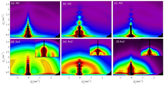
Figure 1.
GISAXS maps of the investigated films. (a–c) Al-based films, (d–f) Au-based films. The insets in (d–f) show simulations of the measured GISAXS maps obtained by their numerical analysis.
The GISAXS maps of the Al-based films are shown in Figure 1a–c and show no signal related to NP formation. The features in the center of their GISAXS maps originate from the coherent scattering, surface roughness and the entire film thickness contributions. These features are not interesting for further analysis of the NP structural and arrangement properties, as the NPs are not formed in the Al-based films according to the GISAXS analysis. It seems that all atoms are homogeneously distributed through the films.
However, the Au-based films, shown in Figure 1d–f, all have a characteristic semicircular (ring-like) signal, which shows the presence of NPs that have a correlated mutual first neighbor spacing (inter-nanoparticle distance). The same type of signal that is present in the Al-based films is present also in the maps of the Au-based films, but as we mentioned before is not interesting for further analysis. The radius of the ring-like signal in the Au-based films decreases with the fraction of Au in the films (Au1–Au3), showing an increase in the distance between the NPs and in the NP size. For the details of the structural properties, we performed a numerical analysis of the GISAXS maps.
The insets show simulations of the measured GISAXS maps obtained by numerical analysis of the GISAXS maps. For the numerical analysis we used the model described in Reference [35]. More precisely, we assumed that NPs order in a 3D paracrystal lattice, described by basis vectors a1–a3. The vectors a1 and a2 are placed in the plane parallel to the substrate surface, while a3 describes the ordering of the NPs in the direction perpendicular to the film surface. We assumed the ordering of the NPs in a body centered tetragonal lattice. A short range ordering is assumed along all basis vectors. The disorder in the NP lattice, i.e., the deviations from the ideal positions defined by basis vectors a1–a3, is described by 4 σ parameters: σ1–2x,y, σ3x,y, σ1–2z and σ1–3z. The first three describe the degree of deviation of the NP positions from the ideal ones in the direction parallel to the film substrate, while the fourth one describes the vertical deviation. The radii of the NPs are denoted by RL and RV for the directions parallel and perpendicular to the film substrate, respectively. The mean radius is denoted by R. The standard deviation of the size distribution is denoted by σR. For more details about the paracrystal lattice and deviation parameters, as well as detailed GISAXS analysis, please see Reference [35]. The results of the numerical analysis are given in Table 2.
Table 2.
Parameters of the Au QD lattices found by GISAXS analysis. a and c are the lateral and vertical separation of Au NPs, respectively; σ1–3x,y,z are the deviation parameters, and RL and RV are the Au NP lateral and vertical radii respectively. All values are given in nm.
The structural properties of the NPs in the Au-based films, given in Table 2, are summarized in Figure 2. From Figure 2a it follows that all structural parameters including the inter-NP separation a, vertical separation c and the NP radii RL and RV all decrease with increasing MoO3 sputtering power, i.e., with decreasing Au percentage in the films. Figure 2b shows the comparison of the Au/MoO3 volume ratio obtained from the GISAXS analysis (parameters of the NP size and arrangement), and from the deposition conditions (sputtering powers of Au and MoO3). The good agreement between these two curves confirms the reliability of the GISAXS analysis.
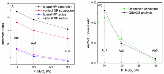
Figure 2.
(a) Structural parameters of the films obtained by GISAXS analysis. (b) Ratio of the volumes of the Au nanoparticles and MoO3 matrix calculated from GISAXS parameters and from the deposition conditions (sputtering powers of Au and MoO3).
The GISAXS analysis shows the decrease of all main NP structural parameters with the sputtering power of MoO3. The increase in the MoO3 sputtering power causes the increase in the number of its atoms on the growing surface during the deposition, while the number of the Au atoms is constant. The increased number of the matrix atoms obviously decreases the diffusion length of the Au atoms resulting in a smaller inter-nanoparticle distance a with increasing MoO3 power. The decrease in the diffusion length also results in the formation of smaller NPs, i.e., in the decrease of RL. The parameters describing the direction perpendicular to the film surface (parameters c and RV) also decrease with the MoO3 sputtering power. The reason is very probably the morphology of the growing surface that influences the self-assembly mechanism (see Reference [36]).
3.1.2. Nanoparticle Internal Structure—Crystalline Properties
The crystalline structure of the films was explored by GIWAXS measurements. The curves measured on Al-based and Au-based films are shown in Figure 3a,b, respectively. The measurements support the GISAXS findings. In the curves of the Al-based films (Figure 3a) there are no Al-related crystalline peaks; however, broad Al2O3-related peaks are weakly observable. Al atoms are therefore very probably oxidized by the oxygen from the MoO3 matrix and residual gas from the deposition chamber, and there is no Al NP formation.
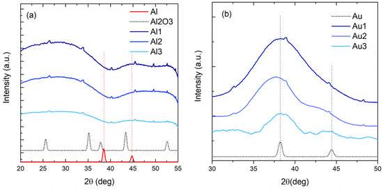
Figure 3.
Grazing-incidence wide angle X ray scattering (GIWAXS) measurements of the (a) Al-based and (b) Au-based films. The tiny peaks with similar shapes, visible in most of the curves, are detector artefacts.
However, the Au-based films (Figure 3b) show clear Au-based (111) and (200) crystalline peaks at 38.1 and 44.3 degrees, respectively. The width of the peaks increases from Au1 to Au3 film, and the (200) peak becomes more visible. The width of the peak is related to the crystallite size; the wider peaks show smaller crystalline grains. Thus, the GIWAXS results show an increase in the Au crystallite size. The Au crystallite radii calculated from the width of the peaks are as follows: 0.7, 0.9 and 1.6 nm for the films Au1, Au2 and Au3, respectively. The obtained values are in good agreement with the Au NP size increase found by GISAXS (Table 2).
3.2. Optical Properties of the Films
The optical properties of the films (absorbance vs. wavelength and energy) are shown in Figure 4. The absorption coefficient of the Al-based films is shown in Figure 4a. Interestingly, the value of the absorbance decreases with an increasing amount of Al (Al1–Al3). The reason could be the formation of Al2O3 in the reaction of Al with O. The refractive index of alumina is lower than that of MoO3 in the measured range of wavelengths [37,38,39], so the increase in the amount of Al2O3 content in the film may reduce the total absorbance of the films, as observed experimentally. This is in agreement with the GIWAXS results that indicate formation of Al2O3 in the Al-based films.
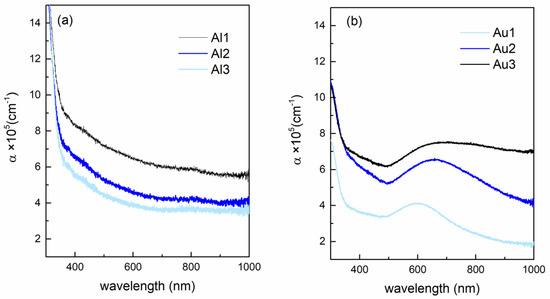
Figure 4.
Optical properties of the films. Absorption coefficient vs. wavelength for (a) Al-based and (b) Au-based films.
The Au-based films show the opposite trend, so the overall absorption coefficient increases with increasing Au content (Au1–Au3) (Figure 4b). Additionally, the Au-based films show the presence of Au surface plasmons, with the maximum close to 580 nm for the film with the smallest Au NPs. The plasmon peak shifts toward higher wavelengths, and it becomes broader with increasing Au NP size. The broadening of the peak is the consequence of the broadening of the Au NP size distribution from A1 to A3 (see the parameter σR, Table 2). Otherwise, the width of the plasmon peak should have the opposite behavior [31,40].
3.3. Electrical Properties of the Films
NPs embedded in oxide matrices are very interesting for nanotechnology applications due to their semiconductor nature, strong confinement effects and dependence of the material properties on the matrix in which the QDs are embedded. Therefore, knowledge of the electrical and transport properties of these materials is essential.
The dependence of the measured resistivity of Al- and Au-based films on the MoO3 deposition power is given in Figure 5. The resistivity of pure MoO3 is about 10 times higher than the highest resistivity of the Al-based film (about 20 MΩcm [41]). It follows from Figure 5a that a decrease of the Al amount causes a drop of the material resistivity. The decrease of the resistivity with the Al content could have a similar origin to doping of some other oxide matrices with Al (like Al-doped ZnO-AZO for example [32]). In the case of AZO, an atomic substitution of Al to Zn in the ZnO crystal structure occurs, which provides a reduction in its electrical resistivity. We also observed a lack of Al nanoparticle formation and a drop in the overall absorption, which supports this assumption. However, a more detailed investigation is needed to explain in detail the effect of Al-doping of MoO3.
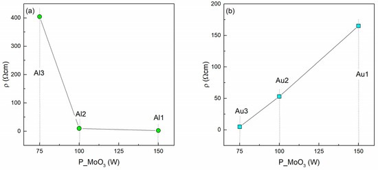
Figure 5.
Resistivity as a function of sputtering power of (a) Al-based and (b) Au-based thin films.
Interestingly, the Au-based films show the opposite trend (Figure 5b). The increase in the proportion of gold in the MoO3 matrix reduces the total resistivity of the films. In the Au-based films Au nanoparticles are formed, so another transport mechanism occurs.
The dependence of the resistivity on the Au NP lattice parameters and Au NP separation are shown in Figure 6a,b, respectively. Figure 6a shows that the resistivity drops with all of the main structural parameters including the mean NP radius R and lateral and vertical NP lattice parameters (a and c, respectively). The more interesting parameter is the Au NP separation, which is calculated from the arrangement parameters of the Au nanoparticles and their radii. The dependence of the resistivity on the Au separation (closest distance to the neighbor) is shown in Figure 6b. From the figure it is evident that the resistivity significantly increases with the NP separation.
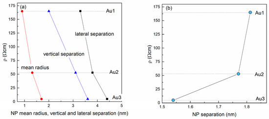
Figure 6.
Resistivity as function of the (a) Au NP lattice parameters, (b) Au NP separation.
Several different transport mechanisms exist to describe the resistivity in quantum dot assemblies including, but not limited to, tunneling and hopping conduction [42]. Based on the results shown in Figure 6b, we believe that the main transport occurs by tunneling of charge carriers through MoO3 barriers between Au NPs [43,44]. In a simplified case, a rectangular potential barrier between NPs is assumed, where the probability of tunneling, and thus the conductivity, decreases exponentially with the nanoparticle distance. We intend to perform a more profound analysis of the transport mechanism on a larger series of samples in our future work.
4. Conclusions
We studied Au+MoO3 and Al+MoO3 thin films prepared by magnetron sputtering codeposition at room temperature. The structural parameters of these films and their main optical and transport properties were explored. We show that Al does not form nanoparticles in the MoO3 matrix, contrary to Au, which produces a 3D lattice of nanoparticles. The dependence of the parameters of the Au NP lattice on the deposition condition is shown. Tuning the deposition conditions, we can tune the size and separation of the Au NPs. The optical properties of the Al- and Au-based films also significantly differ. The Al-based films show a decrease of the absorption with increasing Al content. The Au-based films show the opposite trend, and in addition they show a size-dependent surface plasmon resonance peak. The Al- and Au-based films show opposite behavior of their electrical properties. While the resistivity for the Al-based films increases with the Al content, the resistivity decreases for the Au-based ones. We believe that Al incorporates in the MoO3 lattice, while the electrical transport in Au-based films occurs via tunneling of charge carriers between NPs. The studied material is very interesting for application in various nanotechnology devices.
Author Contributions
Conceptualization, T.C. and M.M.; methodology, T.C., S.B. and M.M.; software, M.M.; formal analysis, I.J., I.Š., M.M.; data curation, I.J., I.Š., S.B.; writing—original draft preparation, T.C. writing—review and editing, all authors.; visualization, T.C. and M.M.; project administration, M.M.; funding acquisition, M.M. All authors have read and agreed to the published version of the manuscript.
Funding
This research was funded by the Croatian Science Foundation (No. IP-2018-01-3633) and the Center of Excellence for Advanced Materials and Sensing Devices (Grant KK.01.1.1.01.0001). This work was supported by the Calipso plus project.
Data Availability Statement
Datasets available at: Mičetić, Maja (2021), “Structural, Optical and Electrical Properties of Al+MoO3 and Au+MoO3 Thin Films Prepared by Magnetron Codeposition”, Mendeley Data, V1, doi: 10.17632/8xdbb452nt.1
Acknowledgments
The authors are thankful to Joško Erceg for the assistance in the sample preparation and Dario Mičetić for GISAXS measurements. The authors acknowledge the CERIC-ERIC Consortium for the access to the experimental SAXS facilities and financial support.
Conflicts of Interest
The authors declare no conflict of interest.
References
- Bouzidi, A.; Benramdane, N.; Tabet-Derraz, H.; Mathieu, C.; Khelifa, B.; Desfeux, R. Effect of substrate temperature on the structural and optical properties of MoO3 thin films prepared by spray pyrolysis technique. Mater. Sci. Eng. B 2003, 97, 5–8. [Google Scholar] [CrossRef]
- Prasad, A.K.; Kubinski, D.J.; Gouma, P.I. Comparison of sol-gel and ion beam deposited MoO3 thin film gas sensors for selective ammonia detection. Sens. Actuators B Chem. 2003, 93, 25–30. [Google Scholar] [CrossRef]
- Ijeh, R.O.; Nwanya, A.C.; Nkele, A.C.; Madiba, I.G.; Bashir, A.K.H.; Ekwealor, A.B.C.; Osuji, R.U.; Ezema, M.M.F. Optical, electrical and magnetic properties of copper doped electrodeposited MoO3 thin films. Ceram. Int. 2020, 46, 10820–10828. [Google Scholar] [CrossRef]
- Li, W.; Cheng, F.; Tao, Z.; Chen, J. Vapor-Transportation Preparation and Reversible Lithium Intercalation/Deintercalation of -MoO3 Microrods. J. Phys. Chem. B 2006, 110, 119–124. [Google Scholar] [CrossRef]
- Wang, B.; Ang, E.H.; Yang, Y.; Zhang, Y.; Geng, H.; Ye, M.; Li, C.C. Interlayer Engineering of Molybdenum Trioxide toward High-Capacity and Stable Sodium Ion Half/Full Batteries. Adv. Funct. Mater. 2020, 30, 2001708–2001718. [Google Scholar] [CrossRef]
- Zhou, C.; Wang, Q.; Yana, X.H.; Wang, J.J.; Wang, D.F.; Yuan, X.X.; Jiang, H.; Zhu, Y.H.; Cheng, X.N. A facile route to synthesize Ag decorated MoO3 nanocomposite for symmetric supercapacitor. Ceram. Int. 2020, 46, 15385–15391. [Google Scholar] [CrossRef]
- Shi, L.; Song, J.; Zhang, Y.; Li, G.; Wang, W.; Hao, Y.; Wu, Y.; Cui, Y. High performance flexible organic photomultiplication photodetector based on ultra-thin silver lm transparent electrode. Nanotechnology 2020, 31, 314001. [Google Scholar] [CrossRef]
- Kim, S.H.; Jang, K.; Kang, P.W.; Ahn, J.-P.; Seol, J.B.; Kwak, C.M.; Hatzoglou, C.; Vurpillot, F.; Choi, P.P. Characterization of Pd and Pd@Au core-shell nanoparticles using atom probe tomography and field evaporation simulation. J. Alloy Compd. 2020, 831, 154721. [Google Scholar] [CrossRef]
- Huo, N.; Kang, J.; Wei, Z.; Li, S.S.; Li, J.; Wei, S.H. Novel and enhanced opto-electronicperformances of multilayer MoS2-WS2 heterostructure transistors. Adv. Funct. Mater. 2014, 24, 7025–7031. [Google Scholar] [CrossRef]
- Saroja, A.P.V.K.; Muthusamy, K.; Sundara, R. Core-Shell Cathode Design with Molybdenum trioxide as Electrocatalytic Trap-ping layer for High Energy Density Room Temperature Sodium Sulfur Bat-tery. J. Phys. Chem. C 2020, 124, 7615–7623. [Google Scholar] [CrossRef]
- Vasanth, A.; Nair, S.V.; Shanmugam, M. Microwave Engineered Structural, Nanomorphological and Photo-responsive Characteristics in 2D-Layered Dual-Phase MoO3-MoSe2 Films. Appl. Surf. Sci. 2020, 519, 146263–146272. [Google Scholar] [CrossRef]
- Naresh, N.; Jena, P.; Satyanarayana, N. Facile synthesis of MoO3/rGO nanocomposite as anode materials for high performance lithium-ion bat-tery applications. J. Alloy Compd. 2019, 810, 151920. [Google Scholar] [CrossRef]
- Zhang, K.; Kotadiya, N.B.; Wang, X.Y.; Wetzelaer, G.-J.A.H.; Marsza-lek, T.; Pisula, W.; Blom, P.W.M. Interlayers for Improved Hole Injection in Organic Field-Effect Transistors. Adv. Electron. Mater. 2020, 6, 1901352. [Google Scholar] [CrossRef]
- Davis, B.A.; Chakrabortyb, B.; Kalarikkala, N.; Ramaniahb, L.M. Room temperature ferromagnetism in carbon doped MoO3 for spintronic applications: A DFT study. J. Magn. Magn. Mater. 2020, 502, 166503. [Google Scholar] [CrossRef]
- Rajendran, R.; Shrestha, L.K.; Minami, K.; Subramanian, M.; Jayavel, R.; Ariga, K. Dimensionally integrated nanoarchitectonics for a novel composite from 0D, 1D, and 2D nanomaterials: RGO/CNT/CeO2 ternary nanocompo-sites with electrochemical performance. J. Mater. Chem. A 2014, 2, 18480–18487. [Google Scholar] [CrossRef]
- Tang, Z.; Lin, J.; Wang, L.; Lv, Y.; Fan, Y.H.Y.; Guo, X.; Zhao, J.; Wangd, Y.; Liu, X. High performance, top-emitting, quantum dot light-emitting diodes with all solution-processed functional layers. J. Mater. Chem. C 2017, 5, 9138. [Google Scholar] [CrossRef]
- Zhu, S.; Song, Y.; Zhao, X.; Shao, J.; Zhang, J.; Yang, B. The photoluminescence mechanism in carbon dots (graphene quantum dots, carbon nanodots, and polymer dots): Current state and future perspective. Nano Res. 2015, 8, 355–381. [Google Scholar] [CrossRef]
- Melanko, J.B.; Pearce, M.E.; Salem, A.K. Nanotubes, nanorods, nanobers, and fullerenes for nanoscale drug delivery. In Nanotechnology Drug Deliver; Springer: New York, NY, USA, 2009; pp. 105–127. [Google Scholar]
- Guan, G.; Han, M.Y. Functionalized Hybridization of 2D Nanomate-rials. Adv. Sci. 2019, 6, 1901837. [Google Scholar] [CrossRef] [PubMed]
- Basioli, L.; Tkalcević, M.; Bogdanović-Radović, I.; Drazić, G.; Nadazdy, P.; Šilović, P.; Salamon, K.; Mičetić, M. 3D Networks of Ge Quantum Wires in Amorphous Alumina Matrix. Nanomaterials 2020, 10, 1363. [Google Scholar] [CrossRef]
- Nekić, N.; Sarić, I.; Salamon, K.; Basioli, L.; Sancho-Parramon, J.; Grenzer, J.; Hubner, R.; Bernstorff, S.; Petravič, M.; Mičetić, M. Preparation of non-oxidized Ge quantum dot lattices in amorphous Al2O3, Si3N4 and SiC matrices. Nanotechnology 2019, 30, 335601. [Google Scholar] [CrossRef]
- Bernstorff, S.; Holy, V.; Endres, J.; Vales, V.; Sobota, J.; Siketić, Z.; Bogdanović-Radović, I.; Buljan, M.; Drazić, G. Co nanocrystals in amorphous multilayers—A structure study. J. Appl. Cryst. 2013, 46, 1711–1721. [Google Scholar] [CrossRef]
- Asaduzzaman, A.M.; Springborg, M. Structural and electronic properties of Si/Ge nanoparticle. Phys. Rev. B 2006, 74, 165406. [Google Scholar] [CrossRef]
- Buljan, M.; Radić, N.; Sancho-Paramon, J.; Janicki, V.; Grenzer, J.; Bogdanović-Radović, I.; Siketić, Z.; Ivanda, M.; Utrobičić, A.; Hubner, R.; et al. Production of three-dimensional quantum dot lattice of Ge/Si core-shell quantum dots and Si/Ge layers in an alumina glass matrix. Nanotechnology 2015, 26, 065602. [Google Scholar] [CrossRef] [PubMed]
- Nekić, N.; Sancho-Paramon, J.; Bogdanović-Radović, I.; Grenzer, J.; Hubner, R.; Bernstorff, S.; Ivanda, M.; Buljan, M. Ge/Si core/shell quantum dots in alumina: Tuning the optical absorption by the core and shell size. Nanophotonics 2017, 6, 1055–1062. [Google Scholar] [CrossRef][Green Version]
- Ray, N.; Gupta, N.; Adhikary, M.; Nekić, N.; Basioli, L.; Drazić, G.; Bernstorff, S.; Mičetić, M. Influence of Structure on Electronic Charge Transport in 3D Ge Nanowire Networks in an Alumina Matrix. Sci. Rep. 2019, 9, 5432. [Google Scholar] [CrossRef]
- Jain, S.; Hirst, D.G.; O’Sullivan, J.M. Gold nanoparticles as novel agents for cancer therapy. Br. J. Radiol. 2012, 85, 101–113. [Google Scholar] [CrossRef]
- Lim, Z.Z.J.; Li, J.E.J.; Ng, C.T.; Yung, L.Y.L.; Bay, B.H. Gold nanoparticles in cancer therapy. Acta Pharmacol. Sin. 2011, 32, 983–990. [Google Scholar] [CrossRef]
- Priyadarshinia, E.; Pradhanab, N. Gold nanoparticles as effcient sensors in colorimetric detection of toxic metal ions: A review. Sens. Act. B Chem. 2017, 238, 888–902. [Google Scholar] [CrossRef]
- Borges, M.; Buljan, J.; Sancho-Parramon, J.; Bogdanović-Radović, I.; Siketić, Z.; Scherer, T.; Kubel, C.; Bernstorff, S.; Cavaleiro, A.; Vaz, F.; et al. Evolution of the surface plasmon resonance of Au:TiO2 nanocomposite thin films with annealing temperature. J. Nanopart. Res. 2014, 16, 2790–2796. [Google Scholar] [CrossRef]
- Amendola, V.; Pilot, R.; Frasconi, M.; Marago, O.M.; Iati, M.A. Surface plasmon resonance in gold nanoparticles: A review. J. Phys. Cond. Mat. 2017, 29, 203002–203040. [Google Scholar] [CrossRef] [PubMed]
- Sukee, A.; Kantarak, E.; Singjai, P. Preparation of Aluminum doped Zinc Oxide Thin Films on Glass Substrate by Sparking Process and Their Optical and Electrical Properties. IOP Conf. Ser. J. Phys. Conf. Ser. 2017, 901, 012153. [Google Scholar] [CrossRef]
- Pan, H.; Zuo, L.; Fan, W.C.; Andreasen, B.; Jiang, X.; Norrm, K.; Krebs, F.C.; Chen, H. MoO3–Au composite interfacial layer for high efficiency and air-stable organic solar cells. Org. Electron. 2013, 14, 797–803. [Google Scholar] [CrossRef]
- Van der Pauw, L.J. A method of measuring the resistivity and Hall coefficient on lamellae of arbitrary shape. Philips Tech. Rev. 1958, 26, 220–224. [Google Scholar]
- Buljan, M.; Radić, N.; Bernstorff, S.; Drazić, G.; Bogdanović-Radović, I.; Holy, V. Grazing-incidence small-angle X-ray scattering: Application to the study of quantum dot lattices. Acta Cryst. A 2012, 68, 124–138. [Google Scholar] [CrossRef] [PubMed]
- Buljan, M.; Desnica, U.V.; Ivanda, M.; Radić, N.; Dubček, P.; Drazić, G.; Salamon, K.; Bernstorff, S.; Holy, V. Formation of three-dimensional quantum-dot superlattices in amorphous systems: Experiments and Monte Carlo simulations. Phys. Rev. B 2009, 79, 035310. [Google Scholar] [CrossRef]
- Vos, M.; Macco, B.; Thissen, N.F.W.; Bol, A.A.; Kessels, W.M.M. Atomic layer deposition of molybdenum oxide from (NtBu)2(NMe2)2Mo and O2 plasma. J. Vac. Sci. Technol. A 2016, 34, 01A103. [Google Scholar]
- de Melo, O.; González, Y.; Climent-Font, A.; Galán, P.; Ruediger, A.; Sánchez, M.; Calvo-Mola, C.; Santana, G.; Torres-Costa, V. Optical and electrical properties of MoO2 and MoO3 thin films prepared from the chemically driven isothermal close space vapor transport technique. J. Phys. Condens. Matter 2019, 31, 295703. [Google Scholar] [CrossRef]
- Malitson, H.; Dodge, M.J. Refractive Index and Birefringence of Synthetic Sapphire. J. Opt. Soc. Am. 1972, 62, 1405. [Google Scholar]
- Farooq, S.; de Araujo, R.E. Engineering a Localized Surface Plasmon Resonance Platform for Molecular Biosensing. Open J. Appl. Sci. 2018, 8, 126–139. [Google Scholar] [CrossRef]
- Subbarayudu, S.; Reddy, K.V.S.; Uthanna, S. Sputtering pressure influenced structural, electrical andoptical properties of RF magnetron sputtered MoO3 films. Mater. Sci. 2000, 38, 41–47. [Google Scholar]
- Car, T.; Santić, A.; Ray, N.; Nekić, N.; Salamon, K.; Bernstorff, S.; Buljan, M. Annealing induced semiconductor-metal transition in Ge+ITO film. Appl. Phys. Lett. 2017, 111, 172104. [Google Scholar] [CrossRef]
- Tackeuchi, A.; Kuroda, T.; Mase, K. Dynamics of carrier tunneling between vertically aligned double quantum dots. Phys. Rev. B 2000, 62, 1568–1571. [Google Scholar] [CrossRef]
- Sinha, A.R.; Roychoudhury, Y.P. Varshni, Wentzel-Kramers-Brillouin quantization rules for two-dimensional quantum dots. Phys. B 2003, 325, 214–223. [Google Scholar] [CrossRef]
Publisher’s Note: MDPI stays neutral with regard to jurisdictional claims in published maps and institutional affiliations. |
© 2021 by the authors. Licensee MDPI, Basel, Switzerland. This article is an open access article distributed under the terms and conditions of the Creative Commons Attribution (CC BY) license (http://creativecommons.org/licenses/by/4.0/).