Hardware Architecture and Cutting-Edge Assembly Process of a Tiny Curved Compound Eye

 and
and
Abstract
: The demand for bendable sensors increases constantly in the challenging field of soft and micro-scale robotics. We present here, in more detail, the flexible, functional, insect-inspired curved artificial compound eye (CurvACE) that was previously introduced in the Proceedings of the National Academy of Sciences (PNAS, 2013). This cylindrically-bent sensor with a large panoramic field-of-view of 180° × 60° composed of 630 artificial ommatidia weighs only 1.75 g, is extremely compact and power-lean (0.9 W), while it achieves unique visual motion sensing performance (1950 frames per second) in a five-decade range of illuminance. In particular, this paper details the innovative Very Large Scale Integration (VLSI) sensing layout, the accurate assembly fabrication process, the innovative, new fast read-out interface, as well as the auto-adaptive dynamic response of the CurvACE sensor. Starting from photodetectors and microoptics on wafer substrates and flexible printed circuit board, the complete assembly of CurvACE was performed in a planar configuration, ensuring high alignment accuracy and compatibility with state-of-the art assembling processes. The characteristics of the photodetector of one artificial ommatidium have been assessed in terms of their dynamic response to light steps. We also characterized the local auto-adaptability of CurvACE photodetectors in response to large illuminance changes: this feature will certainly be of great interest for future applications in real indoor and outdoor environments.1. Introduction
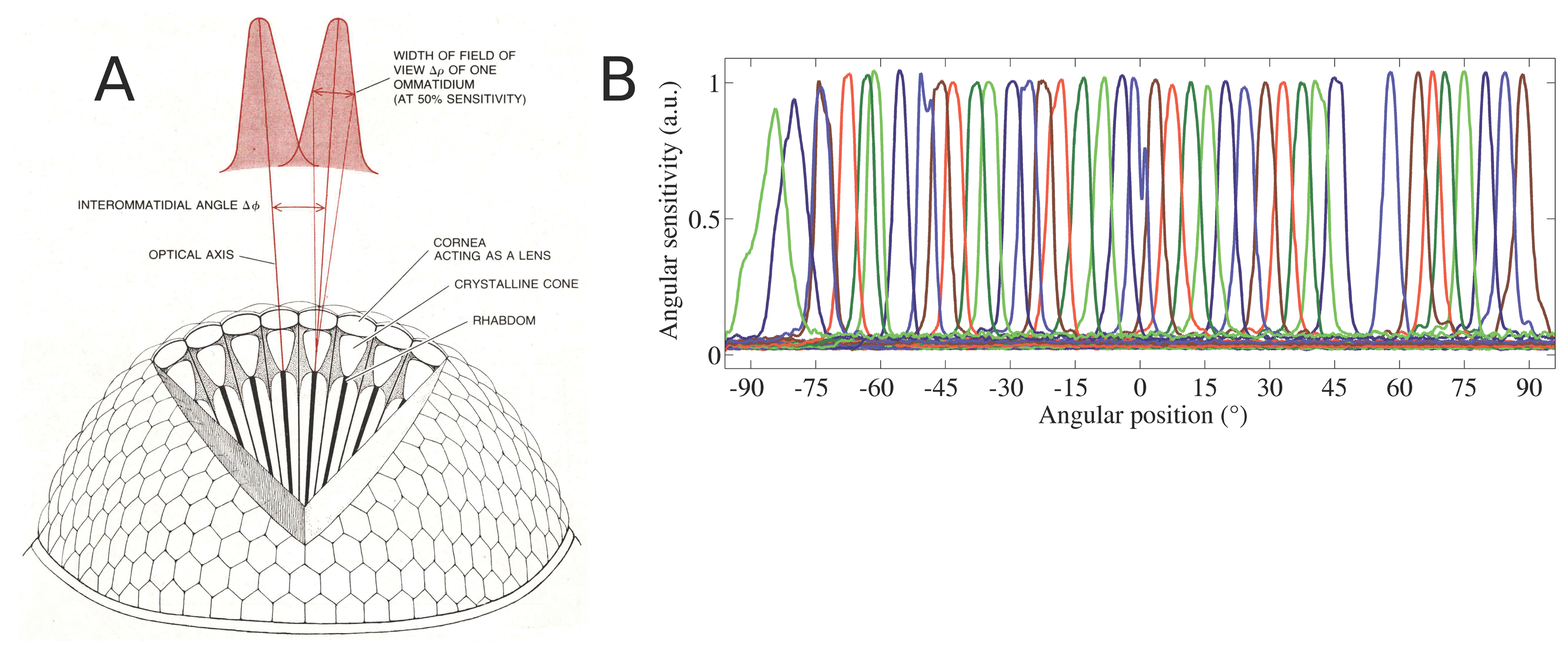
The compound eyes of insects and crustaceans, which show an extraordinarily wide range of designs (see [1] for a review), a remarkable optical layout, high sensitivity in dim light, even at night, and polarized light sensitivity, provide an endless source of inspiration for designing the curved, flexible visual sensors of the future. The paper extends the description of a flexible functional insect-inspired curved artificial compound eye (CurvACE) that was previously introduced by Floreano et al. [2]. In particular, we thoroughly describe here the innovative VLSI sensing layout, the accurate assembly fabrication process, the innovative, fast read-out interface of the sensor, as well as the auto-adaptive dynamic response of the CurvACE photodetectors. Several attempts have been recently made to realize miniature compound eyes. Artificial compound planar eyes based on micro-lens arrays with adjustable optical axes have been developed and interfaced with conventional flat CMOS imagers ([3,4]). However, the optical field of view (FOV) was restricted to a range of ± 30°. To overcome this limitation, micro-optics on curved substrates have been introduced using several methods ([5–7]), including the use of spherical bulk lenses [6], planar wide angle and telescopic lenses ([7,8]), micro-prism arrays [9], a tiny flexible camera array [10] and an origami assembly of 2D optic flow sensors [11]. Small omnidirectional cameras ([12–17]) have been designed for robotic applications. However, correcting the distortion of the optics requires large computational resources and the use of classical imagers restricts the frame rate (e.g., 80 frames per second [15]). The challenge of designing an extremely compact eye with a panoramic visual field can only be met by considering not only the optics, but the whole imaging system. Flexible image sensors inspired by the shape of the retina in the vertebrate single lens eye ([18,19]) and curved optoelectronic cameras with a limited field of view were recently presented ([20–22]). In one case, Song et al. [23] succeeded in bending a stretchable planar compound eye to obtain a spherical compound eye composed of 180 ommatidia with an overall field-of-view of 160° × 160°. This remarkable design is based on cutting-edge technologies, such as flexible micro-lens arrays and micro-electronics (photodiode), encapsulated within a flexible polyimide support. However, this new principle was associated with non-uniform visual sampling, and because of the very coarse resolution of the eye (the interommatidial angle ranged from 8° to 11°), large computational resources were required to put (“stitch”) together the various subimages acquired by the ommatidia. The state-of-the-art technologies based on planar assembly and the use of rigid materials, such as silicon (VLSI chips) and glass (optics), have been applied to obtain a miniature curved compound eye. Moreover, the presented concept allows for the construction of manifold and even extensive bendable multi-channel sensor shapes. In order to enhance the sensing abilities of future robotic platforms, it was proposed to develop a small, lightweight, power-efficient artificial compound eye endowed with an adaptation mechanism right at the photodetector level, which is able to compensate for considerable changes in the ambient light. Visual sensors must be able to deal with the large dynamic range of natural irradiance levels, which can cover approximately up to nine decades during the course of the day. Animal retinae have partly solved this crucial problem, since their photoreceptors implement a light-adaptation mechanism ([24–26]). As described in Section 3, we equipped each CurvACE photodetector with a neuromorphic adaptation circuit [27], which acts within each ommatidium independently of its 629 neighbors. In addition to fast auto-adaptive photodetectors, a fast communication interface was also included, which was able to read the 42 columns of 15 ommatidia at a very high speed (up to 1950 frames per second). Section 2 summarizes the CurvACE features. Section 3 describes in detail the hardware architecture and the patented method [28] used to construct the CurvACE sensor. Section 4 gives results of tests performed on the compound eye in terms of its photodetectors' responses and its auto-adaptive abilities to various lighting conditions.
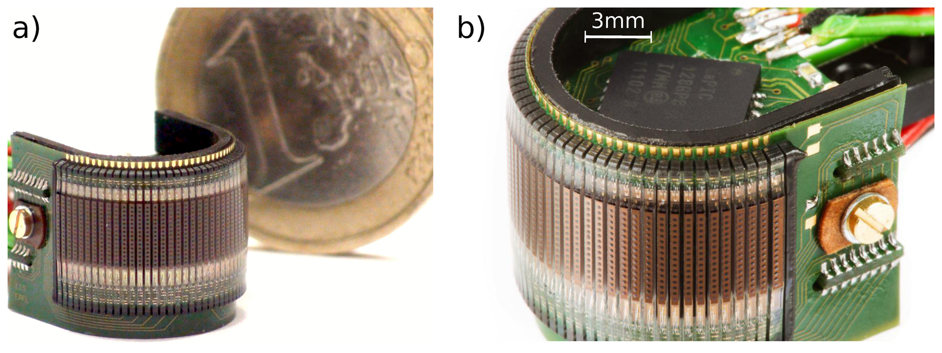
2. Overview of a Miniature Cylindrical Compound Eye
The CurvACE compound eye presented in Figure 1 consists of an ommatidial patch, which has been cylindrically bent and attached to the outside of a curved polymeric scaffold. The ommatidial patch has 630 photodetectors grouped in 42 identical columns of 15 photodetectors (each equipped with its own microoptical lens) which are placed on a thin flexible printed circuit board (PCB) wrapped around the cylindrical scaffold. Interestingly, the whole patch of 630 ommatidia (total thickness 0.85 mm) weighs no more than 0.36 g. Two rigid PCBs bearing signal processing units, which are responsible for the readout of the visual data, have been placed in the concavity space and connected to an external processing unit. Two additional inertial sensors (a three-axis rate gyro and a three-axis accelerometer) were implemented to provide complementary information to visual data. Thanks to this compact mechanical design, the entire device has a volume of only 2.2 cm3 and weighs only 1.75 g. The maximum power consumption of the device is 0.9 W. The readout is performed using a direct serial communication bus that acquires data in parallel from the ommatidial columns. The visual data provided by the columns are serialized at a clock frequency of 1 MHz. The visual data are delivered at a maximum frame rate of about 1950 frame per second (fps), which is suitable for fast optic flow (OF) extraction.
3. Description of the Flexible Ommatidial Patch
3.1. Layout of the Photodetector Layer
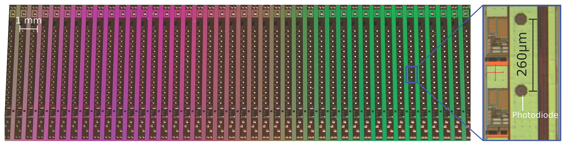
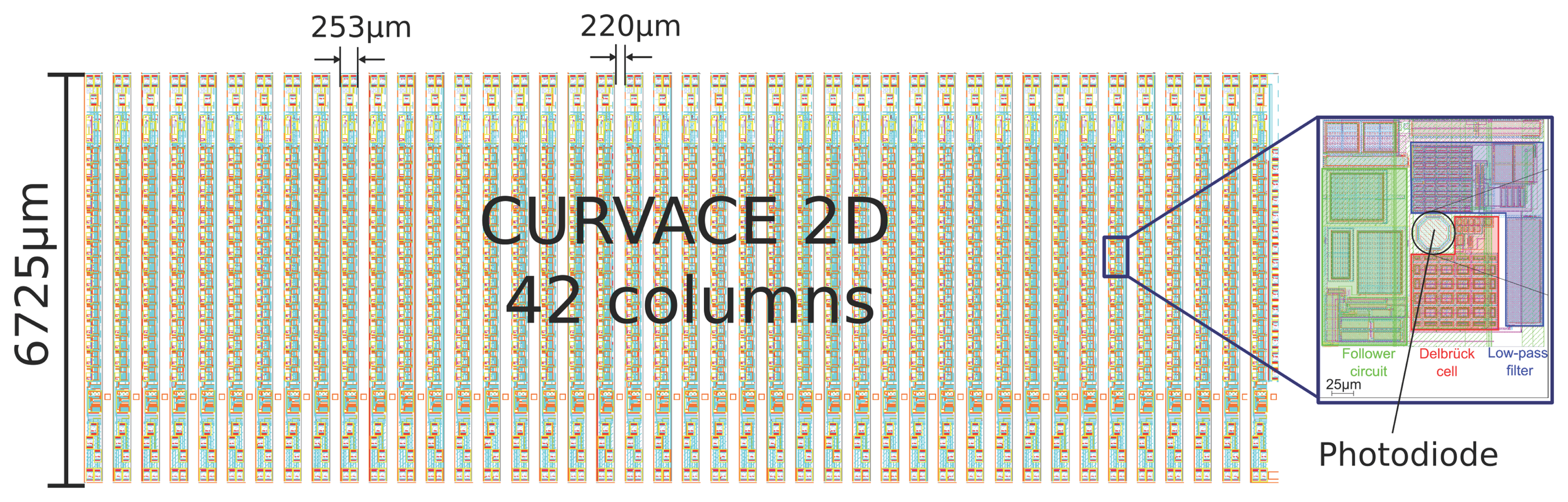
The photodetector array was generated by 0.35 μm CMOS technology with an optoelectronic option (XFAB opto option) giving openings with an anti-reflective coating placed above the photodiode areas. Figures 2 and 3 show the layout of the die with 42 columns having a total lot size of 19.845 by 6.765 mm2. As part of a multi-project wafer, 132 tested dies were received from a complete 200-mm wafer.
In general, the layout is the same for all columns, except the most right one, which possesses additional readout test pads for each photodetector. As shown in Figure 2 and in the Figure S2 of the Supplementary Data published in [2] , a column consists of 15 photodetectors followed by Delbrück circuits [27], a 16-channel multiplexer (MUX), a 10-bit analog-to-digital converter (ADC), a state-machine and eight electro-static discharge (ESD) shielded pads for wire bonding. An additional bias circuit serves to generate the polarization current required by the self-adaptive and low-pass filter circuits integrated at the photodetector level.
The main supply voltage was decoupled and divided into one for the analogue circuitry and another for the digital circuitry (four pads). The further processing of the photodiode output signals via a multiplexer (MUX) and the ADC is shown in Figure 4 (three pads for sync, clock and data lines). The remaining pad is an analogue readout of the central photodetector for testing purposes. Moreover, the left (16th) channel of the MUX is reserved for a reference voltage. The width of the self-contained column's circuitry is 253 μm, whereas the space to its neighbors is 220 μm. These gaps are mandatory for later separation issues and consider clearance areas due to possible damaging of the die. This gives a column pitch of 473 μm. Each column contains 15 octagonal Nwell-Psubstrate photodetectors with a diameter of 30 μm. The photodiodes are aligned in the column with a vertical spacing of 260 μm.
3.2. CurvACE Readout Interface
The specifications of the readout interface were very drastic in terms of the number of pads (minimum number of pads per column), bit rate (as fast as possible) and resources available (no flash or Electrically-erasable programmable read-only memory (EEPROM) available for storing an address). Several communication standards were considered for use in CurvACE: the main characteristics of the bus interfaces are summarized in Table 1.
The selected “direct connection protocol” (DCP) is based on:
a single clock signal sent to each column,
a sync signal used to start the conversion of the associated columns,
a digital-out signal (Dout) per column used for the serial transfer of each pixel output signal.
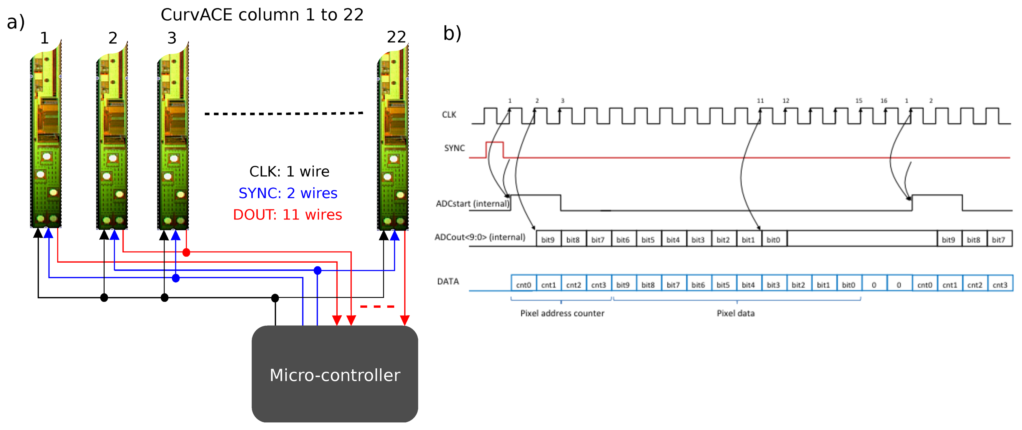
The main advantage of this protocol is that it does not require any addresses (stored in an EEPROM memory, for example) to be able to communicate with a column. Besides, the refresh rate does not depend on the number of columns, and the readout protocol adds only three pads per column, which leads to eight pads in total:
a digital-out signal (Dout) per column used for the serial transfer of each pixel output signal,
four pads for the digital (Dvdd) and analog (Avdd ) power sources and for the ground (DGnd and AGnd),
three pads (see Figure 4a) for the serial readout (Clock, Sync, Dout),
1 test pad.
At the beginning of each conversion cycle (see Figure 4b), the counter value corresponding to the pixel address is added to the output data. The data is transferred serially through the output shift register during the ADC conversion. Individual bits resulting from the ADC conversion are validated before the end of the ADC conversion. This strategy minimizes the dead time possibly elapsing during the data transfer. At each conversion cycle, 16 bits are sent (four from the counter, 10 from the ADC and two unused bits set at zero) to the external microcontroller. When operating at the maximum sampling frequency of 1 MHz, the ADC therefore provides a maximum sampling rate of about four ksamples/s per photodetector. However, to reduce the number of tracks in the flexible PCB, we decided to use two synchronization signals: one for each group of 21 columns. The maximum sampling rate for reading the 630 ommatidia of the CurvACE sensor was therefore 1950 fps.
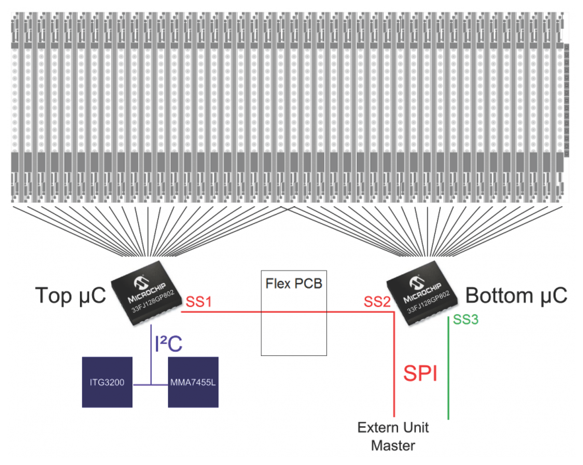
As shown in Figure 5, two dsPIC33FJ128GP802 microcontrollers from Microchip have been applied for the readout and on-site processing of the data. This microcontroller model has 16 kbyte of RAM, although it measures only 6 by 6 mm2. Each micro-controller is responsible for reading out 22 columns (the two central columns were read by both micro-controllers) sequentially by two batches of 11 columns, as we used two synchronization signals. For the readout, a serial direct communication protocol was used. This protocol scans the pixels in every column serially, whereas the columns are read in parallel via 11 data lines connected to each microcontroller (cf. Figures 4 and 5). One of the microcontrollers masters the direct connection protocol and generates the clock and the synchronization signals, which are shared by the other for the sake of synchronization. The microcontrollers themselves communicate via Serial Peripheral Interface (SPI) bus with an external unit, which can be placed on a robot, as well.
The communication protocol of the SPI interface was designed such that data can be extracted from different ROIs (regions of interest) of the CurvACE sensor specified by the user. Only the pixels corresponding to the chosen regions of interest are transmitted to the external unit. After choosing the number of regions of interest and their size, the protocol allows for the following options:
frame rate up to the maximal theoretical frame rate of the sensor, namely 1950 fps,
sampling frequency of the inertial sensor data, which is up to one data per frame,
number of frames that are sent in two separate 16-bit words: 232 frames can be sent with the same configuration.
3.3. Micro-Optics
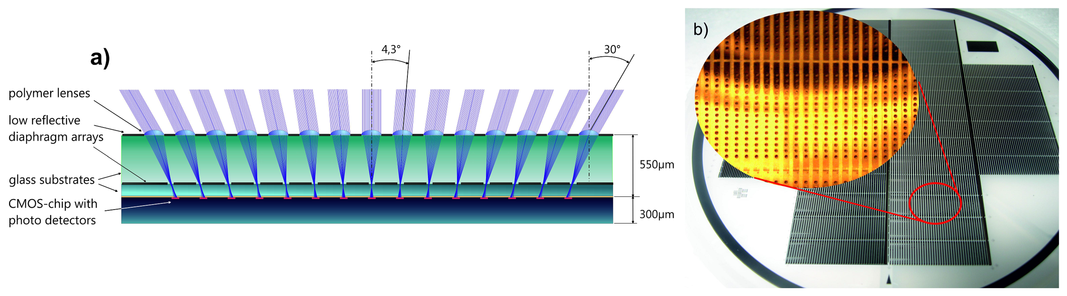
A well-adapted micro-optical system has been mounted onto the photodetector array in order to sample the specified total field of view (FOV) of 180° by 60° by the individual detectors, having a constant acceptance angle of 4.3°. This has been achieved by a multi-aperture approach implying the use of a microlens array [29,30]. To have a gapless registration of FOV, the difference in the chief ray angle between adjacent detectors is set equal to the full-width at half-height (FWHM) of the angular sensitivity function (ASF) of the optical channels. Thus, the ASFs overlap slightly by an intended amount (see Figure 7b). A horizontal FOV of 180° was achieved by the subsequent bending of the assembled sensor device, whereas a vertical FOV of 60° along a single column was obtained by introducing a pitch difference (see Figure 6) between the microlens (pitch of 290 μm) and the photodetector arrays (pitch of 260 μm). Furthermore, the use of toroidal-shaped microlenses reduces aberrations from off-axis imaging [31]. The micro-optics intends to form a Gaussian intensity distribution at the photodetector plane due to the slight defocussing (see Figure 7b). Such deliberate blurred spots have been observed in natural compound eyes, as well (see Figure 7a) and are beneficial for the detector characteristics and the optical flow processing. As pointed out by Lucas and Kanade [32], smoothing the image suppresses small details (i.e., high spatial frequencies) and, thus, improves the convergence of the algorithm once initialized.
The micro-optics have been fabricated in wafer scale utilizing 100-mm substrates of display glass (Schott, D263T). Microlens masters have been generated by reflow of patterned photoresist and replicated by using highly transparent UV-curable organic-inorganic hybrid material (MRT GmbH, Ormocomp). Besides an aperture defining diaphragm array close to the microlens layer, a second diaphragm array is introduced close to the focal plane in order to prevent crosstalk between neighboring channels and to reduce ghost images. The layers are composed of lithographically patterned low-reflective metal (black chromium). The optical stack has a total thickness of about 570 μm, including the sag heights of the microlenses.
3.4. Sensor Assembly
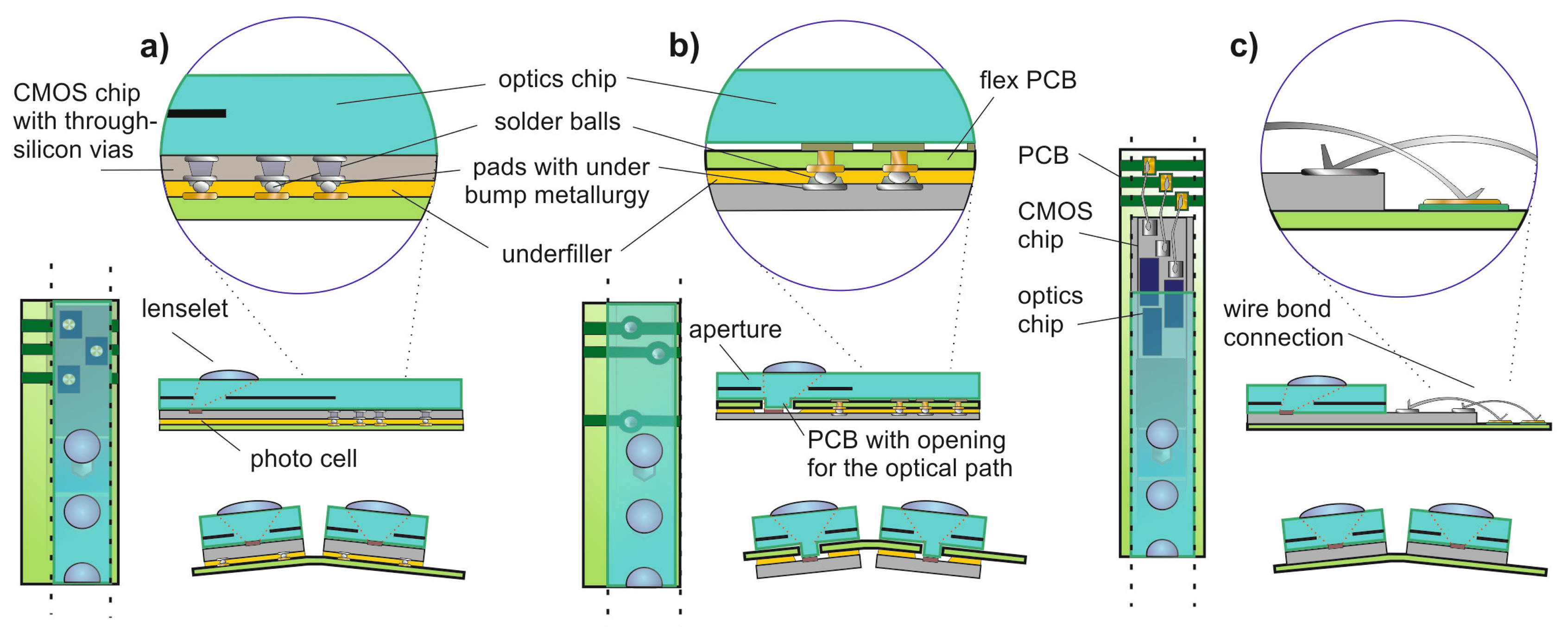
Since the custom designed CMOS Opto-ASICs have been produced on multi-project wafers, a wafer-level bonding of multi-aperture microoptics and sensors was not an option. Consequently, the optics have been bonded chip-wise by using active alignment techniques. Three different assembling concepts were evaluated for prototype fabrication with the potential for small series production (see Figure 8):
Flip chip bonding based on through silicon vias (TSVs). This solution, particularly suitable for mass production, has been dropped as a matter of costs and available space (see Figure 8a).
Flip chip bonding with intermediate flexible PCB. This solution uses conventional top-side electrical contacts, but introduces openings of the PCB located in the middle position between the sensor and optics. Noteworthy, this implied a further adaptation of optics and increased complexity (see Figure 8b).
Wire bonding of the VLSI chip to the flexible PCB. This solution has been chosen due to the comparatively simple stack assembly of the optics, VLSI chip and flexible PCB. Moreover, wire bonding of dies in multi-chip modules is state-of-the-art, even on flexible PCBs (see Figure 8c).
In the first step, the required components have been prepared for stack mounting. The VLSI and the microoptics chips have been diced from eight-inch and four-inch wafers, respectively. Moreover, the sensor chips have trenching grooves at their backside at the positions of the dicing lanes. These trenches of 100 μm in depth and 150 μm in width allowed for safe cutting at a later step.
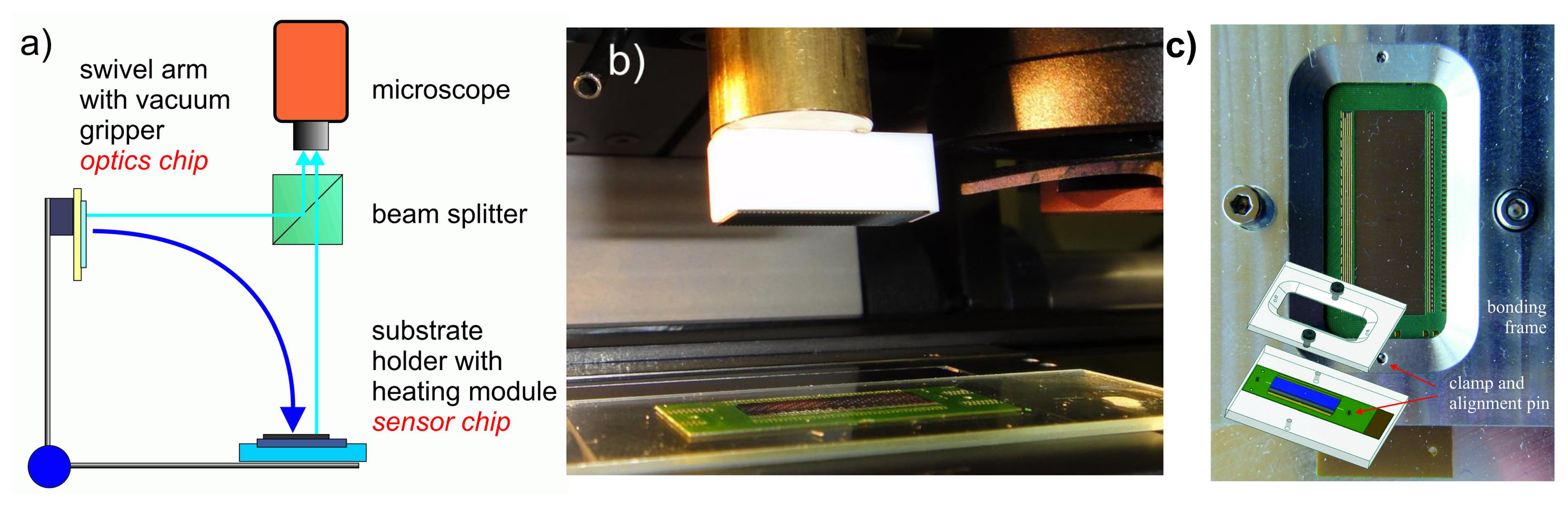
The flexible PCBs were fabricated by fine line technology with gold-plated bond pads. As an alignment aid for the positioning of the sensor-optics stacks, a window of the size of the chip has been left free in the solder mask layer. This enables a placement of the stack within a tolerance of ±20 μm, which holds for bond pad openings and is required for wire bonding. As shown in Figure 9a,b, the adhesive bonding of the multi-aperture optics and CMOS chip was done by a FINEPLACER® lambda device using active alignment and an adapted vacuum gripper for the former of both [35]. The applied transparent UV-curable adhesive (EPO-TEK®OG 146) features high mechanical strength and heat resistance beyond 150 °C, which are appropriate for loads during column separation (shear forces) and encapsulation (heat), respectively. The accuracy of positioning (±1.5 μm) was better than the one requested by the optic design (±3 μm).
In contrast, the mounting of this stack onto the flexible PCB was done passively with a jig aid by means of two-component epoxy glue (EPO-TEK 353ND). Therefore, an adapted assembly stage was used, which allowed for a fast bonding process at an adequate lower level of precision due to a mechanical guide pin (see Figure 9c).
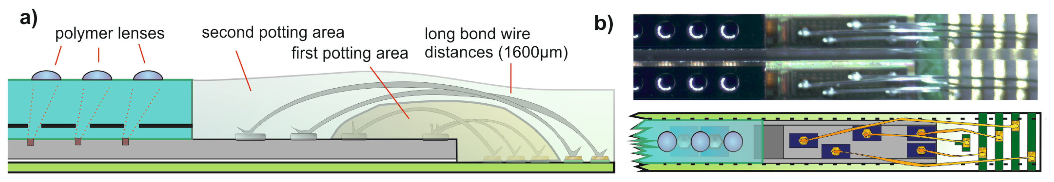
The analog-digital circuit and the readout interface lead to eight interconnection pads per column that are grouped in three and five pads (see Figure 10) at the top and bottom sides, respectively, leading to a total number of 336 interconnections. Due to the column width of 240 μm, five pads cannot be placed side by side, and a two-step bonding was performed, which implies an intermediate potting step of the first set of short wires. A final encapsulation covers all bonding wires, but does not spill over the optics. A previously placed polymer frame on the PCB enclosed the area for casting. During wire bonding and encapsulation, a special bonding frame (see Figure 11a) fixed the PCB to the stage and avoided detachments from pulling forces when the bond head lifts.
Finally, precision cut-off by grinding has been applied to separate the sensor array into 42 equal columns of 15 photodetectors (see Figure 11b). Currently, the sawing technology is the most promising way for efficiently cutting the stack of glass, silicon and polymer (glue and glob-top material) of about 870 μm. Synthetic-resin-compound diamond saw blades of 100 μm in thickness were employed. The backside trenches ensured that the PCB was not touched by the sawing blade and remained intact. Nevertheless, residual glue in the gap between sensor and PCB causes stiffening and impedes its bending. Consequently, an optimized glue thickness is inevitable to prevent uncontrolled breaks and irregular bending. Moreover, it is important to bend it exactly along its designated direction; see Figure 11c. Any torsion may cause a breaking of the columns. Two screws were used to fix the bent PCB to the scaffold of a pre-defined curvature.
4. VLSI Implementation and Dynamic Responses of the CurvACE Auto-Adaptive Photodetectors
4.1. Description of the VLSI Circuit
The CurvACE photodetector is based on an octagonally-shaped Nwell-Psubstrate photodiode with a diameter of 30 μm and on the Delbrück adaptive photodetector cell. It has been shown that a photodiode with an octagonal shape has better sensitivity than a square-shaped one [36]. A low-pass filter next in line limits the cut-off frequency of the photodetector to a value (300 Hz) that is compatible with the sampling rate of the 10-bit ADC used to digitize each photodetector's output signal. The square footage of the circuitry of a single photodetector measures 253 μm by 250 μm.
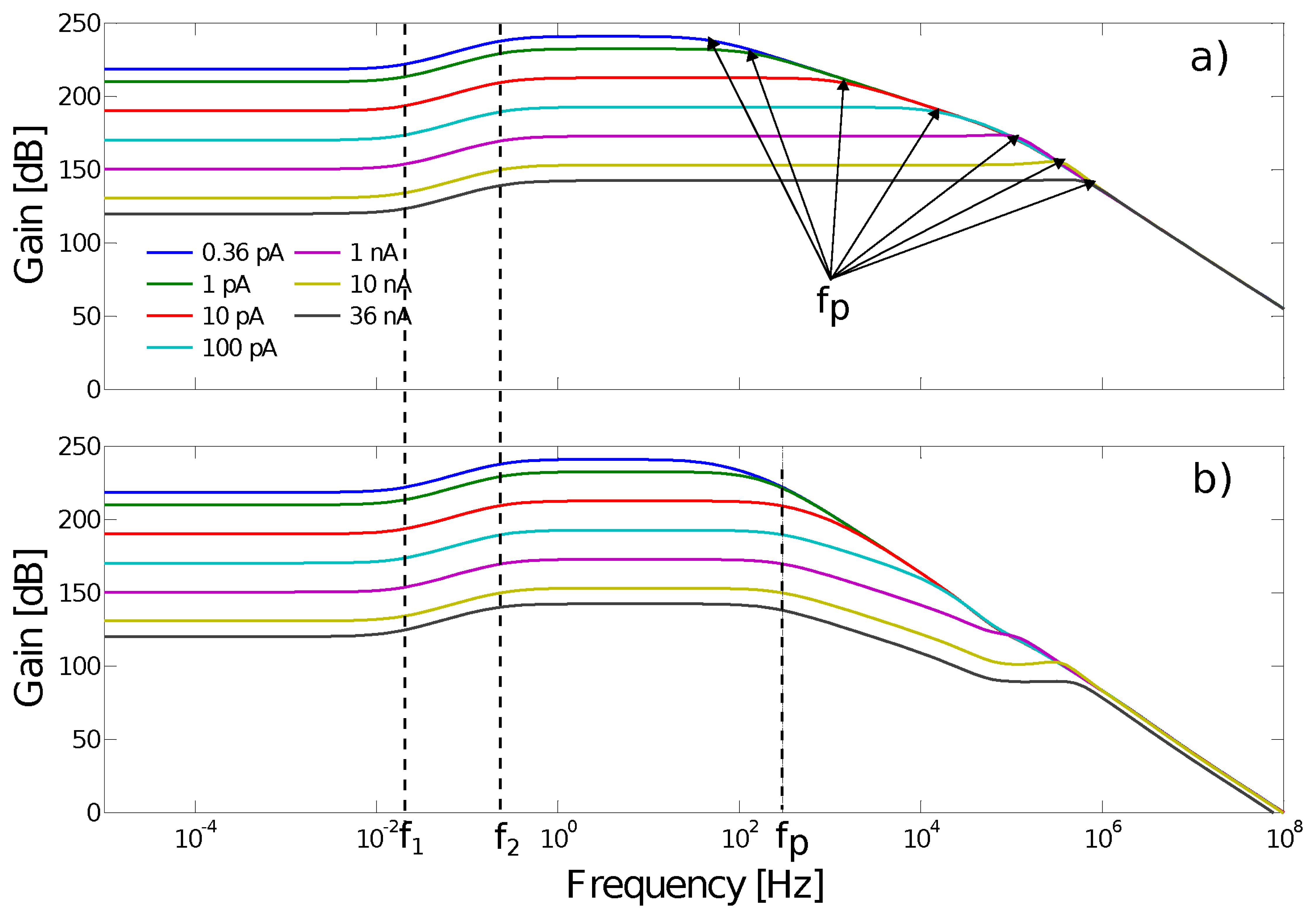
The Delbrück adaptive photodetector consists of a logarithmic circuit associated with a high gain negative feedback loop, as shown in Figure 12. It is based on a MOSFET feedback (MFB) transistor operating in the sub-threshold region where the current-to-voltage characteristic shows logarithmic variations in a large dynamic range of up to several decades. The adaptive element responsible for the DC output levels acts like a very high resistance and makes the output signal Vout follow the gate voltage of the MFB transistor. The non-linear resistance of the adaptive element decreases in the case of fast transient signals. The adaptation to variations in the ambient light levels is therefore relatively slow, whereas the compensations for changes in contrast are much faster (see Section 4.2).
The simulated AC gains obtained with various photodiode background currents are illustrated in Figure 13. The frequencies f1 and f2 are those of the adaptive elements with the two time constants τ defined as follows:
where R is the equivalent resistance of the adaptive element, corresponding to a value of 3.1012 Ω in the case of a low input level, C2 is set at 105 fF, the capacitance ratio is equal to 15 and the frequencies f1 and f2 are equal to approximately 0.03 Hz and 0.5 Hz.
The low-pass cut-off frequency (fp) of the photodetector depends on the background current (i.e., the ambient luminosity). It can be estimated using the following equation:
Therefore, fp varies in a large range from 24 Hz to 2.4 MHz in the 1 Lux to 105 Lux illuminance range.
The output signal of each photodetector is sampled by the ADC at a sampling rate of about 2000 samples/s. However, as shown in Figure 13a, the high cut-off frequency of the photoreceptor can be much greater than 1 kHz at high levels of luminosity. To keep the high cut-off frequency of the auto-adaptive circuit of each photodetector constant, an anti-aliasing filter was implemented by cascading a first order low-pass filter based on a gm-C filter [37]. A high capacitance was directly integrated into the pixels, and the transconductance amplifier (OTA) was biased at a very low current level. The resulting cut-off frequency remained constant and equal to 300 Hz, regardless of the illuminance.
At last, as shown in Figure 12, a follower stage based on an operational amplifier was introduced between the anti-aliasing filter and the ADC to reduce the input time constant and, thus, to improve the accuracy required by the sampling rate of 2 ksamples/s.
The third and last layer of metallization was dedicated to power lines. The photodetector layout is compatible with the low resistivity of the power lines, leading to a low dropout voltage along these lines, as well as a good match between pixels.
4.2. Characterization of the Auto-Adaptive Photodetectors
The auto-adaptive photodetectors were designed to ensure low sensitivity to ambient lighting changes and high sensitivity to the contrasts. Figure 14 shows the dynamic gain adjustment of one CurvACE element (photodetector equipped with optics) facing a set of still or moving strips placed 195 mm from the device. It is obvious that the Delbrück pixel compensates quickly within 400 ms for any sharp change in the illuminance induced by opening a sun-blind manually. Even at low illuminance levels, the signal-to-noise ratio (37.3 dB or 45.3 dB depending on the illuminance level, which was equal to 350 Lux or 380 Lux, respectively) was sufficient for the visual processing algorithms. The noise was measured at an illuminance level of 190 Lux (see Figure 14a).
4.3. Imaging Characteristics of the CurvACE Compound Eye
Figure 15b shows the image produced by the CurvACE prototype when it was rotating at an angular speed of 125°/s, and the images were acquired at a rate of 25 fps. Despite the relatively coarse resolution, the CurvACE sensor was able to produce images of a sufficiently good quality for the pattern to be recognizable. This experiment was repeated with several levels of background illuminance ranging from 0.5 Lux to 1500 Lux in order to test the ability of the CurvACE sensor to compensate for changes in the illuminance. As shown in Figure 15 and as expected from the experimental data shown in Figure 14, no significant differences were observed between the images obtained.
5. Conclusion
The prototype of a compact cylindrically-shaped artificial compound eye was presented, which is suitable for optic flow-based navigation. The well-designed quality of the ommatidia acceptance angles and interommatidial angles lead to a wide, gapless and distortion-free field of view of 180° by 60°. The sampling angle of the 630 ommatidia is about 4.2°. Moreover, it is straightforward to achieve a 360° panorama view by combining two CurvACE devices or two microoptics-CMOS stacks onto an extended flexible PCB. In this paper, we showed, for the first time, the dynamical response at the photoreceptor level (Bode diagram and time response) and provided examples of full resolution images acquired by CurvACE while the latter was stimulated by a moving pattern under different lighting conditions. CurvACE benefits from the use of auto-adaptive photodetectors, which lead to high sensitivity for fast changing contrasts, while adapting to slow variations of background illumination over four decades from 0.5 Lux (moon night) to 1500 Lux (sunny day). An extra low-pass filter was incorporated to maintain a constant cut-off frequency independent of the illuminance level. Another advantage compared to standard CMOS camera sensors is the high sampling rate, which allows a readout of up to 1950 fps. The versatile approach makes use of rigid materials (silicon and glass) and planar assembly technology, which enables high alignment accuracy for established state-of-the-art fabrication processes that could be set-up in a large scale, i.e., micro-optics fabrication, wire bonding and precision cut-off grinding for column separation. Nevertheless, this concept can be adapted to a wide range of shapes, photoreceptor layouts or optical assembly. Such optic flow extracting sensors may find their application in autonomous robots and vehicles. In addition, CurvACE could offer unique opportunities to suggest new explanations for animals' outstanding performances in tasks, such as navigation, obstacle avoidance or chasing and, thus, help to foster the development of novel visual processing algorithms. Future improvements in the design of the compound eye may result in devices with even smaller packages, induced by progress, for example, in CMOS fabrication, processing optical materials or precision cut-off grinding.
Acknowledgments
We thank Jean-Christophe Zufferey and Jacques Duparré for conceptual suggestions; Andreas Mann for the sensor module preparation; and Marc Boyron and Julien Diperi for test bench realization. We also thank the referees for their useful comments. The CurvACE project acknowledges the financial support of the Future and Emerging Technologies (FET) program within the Seventh Framework Programme for Research of the European Commission, under FET-Open Grant 237940. This work also received financial support from the Swiss National Centre of Competence in Research Robotics, the French National Center for Scientific Research (CNRS) and Aix-Marseille University, the French National Research Agency (ANR) with the Entomoptere Volant Autonome (EVA), Intelligent Retina for Innovative Sensing (IRIS) and Equipex/Robotex projects (EVA project and IRIS project under ANR Grant Numbers ANR608-CORD-007-04 and ANR-12-INSE-0009, respectively) and the German Federal Ministry of Education and Research.
Author Contributions
Dario Floreano, Stéphane Viollet, Andreas Brückner, Franck Ruffier and Nicolas Franceschini designed the research. Ramon Pericet-Camara, Robert Leitel, Wolfgang Buss, Felix Kraze, Mohsine Menouni, Fabien Expert, Raphaël Juston, Géraud L'Eplattenier, Fabien Colonnier and Patrick Breugnon performed the research. Stéphane Viollet, Franck Ruffier, Robert Leitel, Wolfgang Buss, Mohsine Menouni, Fabien Expert, Raphaël Juston and Géraud L'Eplattenier contributed with technical and analytic tools. Dario Floreano, Ramon Pericet-Camara, Stéphane Viollet, Franck Ruffier, Andreas Brückner, Robert Leitel, Wolfgang Buss, Mohsine Menouni, Fabien Expert, Raphaël Juston, Hanspeter Mallot and Nicolas Franceschini analyzed the data. Stéphane Viollet, Franck Ruffier, Robert Leitel, Wolfgang Buss, Stéphanie Godiot, Mohsine Menouni and Ramon Pericet-Camara wrote the paper.
Conflicts of Interest
The authors declare no conflict of interest.
References
- Land, M.F.; Nilsson, D.E. Animal Eyes; Oxford University Press: Oxford, UK, 2012. [Google Scholar]
- Floreano, D.; Pericet-Camara, R.; Viollet, S.; Ruffier, F.; Brückner, A.; Leitel, R.; Buss, W.; Menouni, M.; Expert, F.; Juston, R.; et al. Miniature curved artificial compound eyes. Proc. Natl. Acad. Sci. 2013, 110, 9267–9272. [Google Scholar]
- Brückner, A.; Duparré, J.; Bräuer, A.; Tünnermann, A. Artificial compound eye applying hyperacuity. Opt. Express 2006, 14, 12076–12084. [Google Scholar]
- Duparré, J.; Wippermann, F.; Dannberg, P.; Bräuer, A. Artificial compound eye zoom camera. Bioinspir. Biomim. 2008, 3. [Google Scholar] [CrossRef]
- Jeong, K.H.; Kim, J.; Lee, L.P. Biologically Inspired Artificial Compound Eyes. Science 2006, 312, 557–561. [Google Scholar]
- Radtke, D.; Duparré, J.; Zeitner, U.D.; Tünnermann, A. Laser lithographic fabrication and characterization of a spherical artificial compound eye. Opt. Express 2007, 15, 3067–3077. [Google Scholar]
- Qu, P.; Chen, F.; Liu, H.; Yang, Q.; Lu, J.; Si, J.; Wang, Y.; Hou, X. A simple route to fabricate artificial compound eye structures. Opt. Express 2012, 20, 5775–5782. [Google Scholar]
- Kinoshita, H.; Hoshino, K.; Matsumoto, K.; Shimoyama, I. Thin compound eye camera with a zooming function by reflective optics. Proceedings of the 18th IEEE International Conference on Micro Electro Mechanical Systems MEMS 2005, Miami Beach, FL, USA, 30 January–3 Febuary 2005; pp. 235–238.
- Li, L.; Yi, A.Y. Development of a 3D artificial compound eye. Opt. Express 2010, 18, 18125–18137. [Google Scholar]
- Aldalali, B.; Fernandes, J.; Almoallem, Y.; Jiang, H. Flexible Miniaturized Camera Array Inspired by Natural Visual Systems. Microelectromech. Syst. J. 2013, 22, 1254–1256. [Google Scholar]
- Park, S.; Cho, J.; Lee, K.; Yoon, E. 7.2 243.3 pJ/pixel bio-inspired time-stamp-based 2D optic flow sensor for artificial compound eyes. Proceedings of 2014 IEEE International Solid-State Circuits Conference Digest of Technical Papers (ISSCC), San Francisco, CA, USA, 9–13 Febuary 2014; pp. 126–127.
- Humbert, J.; Murray, R.; Dickinson, M. A Control-Oriented Analysis of Bio-inspired Visuomotor Convergence. Proceedings of the 2005 European Control Conference 44th IEEE Conference on Decision and Control (CDC-ECC '05), Seville, Spain, 12–15 December 2005; pp. 245–250.
- Ferrat, P.; Gimkiewicz, C.; Neukom, S.; Zha, Y.; Brenzikofer, A.; Baechler, T. Ultra-miniature omni-directional camera for an autonomous flying micro-robot. Proc. SPIE 2008, 7000. [Google Scholar] [CrossRef]
- Riley, D.T.; Harmann, W.M.; Barrett, S.F.; Wright, C.H.G. Musca domestica inspired machine vision sensor with hyperacuity. Bioinspir. Biomim. 2008, 3. [Google Scholar] [CrossRef]
- Stürzl, W.; Boeddeker, N.; Dittmar, L.; Egelhaaf, M. Mimicking honeybee eyes with a 280° field of view catadioptric imaging system. Bioinspir. Biomim. 2010, 5. [Google Scholar] [CrossRef]
- Luke, G.; Wright, C.H.G.; Barrett, S. A Multiaperture Bioinspired Sensor with Hyperacuity. Sens. J. IEEE 2012, 12, 308–314. [Google Scholar]
- Dong, F.; Ieng, S.H.; Savatier, X.; Etienne-Cummings, R.; Benosman, R. Plenoptic cameras in real-time robotics. Int. J. Robot. Res. 2013, 32, 206–217. [Google Scholar]
- Dinyari, R.; Rim, S.B.; Huang, K.; Catrysse, P.B.; Peumans, P. Curving monolithic silicon for nonplanar focal plane array applications. Appl. Phys. Lett. 2008, 92. http://dx.doi.org/10.1063/1.2883873. [Google Scholar]
- Xu, X.; Davanco, M.; Qi, X.; Forrest, S.R. Direct transfer patterning on three dimensionally deformed surfaces at micrometer resolutions and its application to hemispherical focal plane detector arrays. Organ. Electron. 2008, 9, 1122–1127. [Google Scholar]
- Ko, H.C.; Stoykovich, M.P.; Song, J.; Malyarchuk, V.; Choi, W.M.; Yu, C.J.; Geddes, J.B., III; Xiao, J.; Wang, S.; Huang, Y.; et al. A hemispherical electronic eye camera based on compressible silicon optoelectronics. Nature 2008, 454, 748–753. [Google Scholar]
- Jung, I.; Xiao, J.; Malyarchuk, V.; Lu, C.; Li, M.; Liu, Z.; Yoon, J.; Huang, Y.; Rogers, J.A. Dynamically tunable hemispherical electronic eye camera system with adjustable zoom capability. Proc. Natl. Acad. Sci. 2011, 108, 1788–1793. [Google Scholar]
- Dumas, D.; Fendler, M.; Berger, F.; Cloix, B.; Pornin, C.; Baier, N.; Druart, G.; Primot, J.; le Coarer, E. Infrared camera based on a curved retina. Opt. Lett. 2012, 37, 653–655. [Google Scholar]
- Song, Y.M.; Xie, Y.; Malyarchuk, V.; Xiao, J.; Jung, I.; Choi, K.J.; Liu, Z.; Park, H.; Lu, C.; Kim, R.H.; et al. Digital cameras with designs inspired by the arthropod eye. Nature 2013, 497, 95–99. [Google Scholar]
- Normann, R.A.; Perlman, I. The effects of background illumination on the photoresponses of red and green cones. J. Physiol. 1979, 286, 491–507. [Google Scholar]
- Laughlin, S.B. The role of sensory adaptation in the retina. J. Exp. Biol. 1989, 146, 39–62. [Google Scholar]
- Gu, Y.; Oberwinkler, J.; Postma, M.; Hardie, R.C. Mechanisms of light adaptation in Drosophila photoreceptors. Curr. Biol. 2005, 15, 1228–1234. [Google Scholar]
- Delbrück, T.; Mead, C. Adaptive photoreceptor with wide dynamic range. Proceedings of 1994 IEEE International Symposium on Circuits and Systems (ISCAS '94), London, UK, 30 May–2 June 1994; 4, pp. 339–342.
- Duparré, J.; Brückner, A.; Wippermann, F.; Zufferey, J.C.; Floreano, D.; Franceschini, N.; Viollet, S.; Ruffier, F. Artificial Compound Eye and Method for Fabrication. Patent EP09/012409.0, 2009. [Google Scholar]
- Duparré, J.; Dannberg, P.; Schreiber, P.; Bräuer, A.; Tünnermann, A. Artificial Apposition Compound Eye Fabricated by Micro-Optics Technology. Appl. Opt. 2004, 43, 4303–4310. [Google Scholar]
- Duparré, J.W.; Wippermann, F.C. Micro-optical artificial compound eyes. Bioinspir. Biomim. 2006, 1, R1–16. [Google Scholar]
- Duparré, J.; Wippermann, F.; Dannberg, P.; Reimann, A. Chirped arrays of refractive ellipsoidal microlenses for aberration correction under oblique incidence. Opt. Express 2005, 13, 10539–10551. [Google Scholar]
- Lucas, B.D.; Kanade, T. An iterative image registration technique with an application to sereo vision. Proceedings of 7th International Joint Conference on Artificial Intelligence, Vancouver, BC, Canada, 24–28 August 1981; pp. 121–130.
- Stavenga, D.G. Angular and spectral sensitivity of fly photoreceptors. I. Integrated facet lens and rhabdomere optics. J. Comp. Physiol. A Neuroethol. Sens. Neural Behav. Physiol. 2003, 189, 1–17. [Google Scholar]
- Horridge, G.A. The compound eye of insects. Sci. Am. 1977, 237, 108–120. [Google Scholar]
- Buss, W.; Kraze, F.; Bruckner, A.; Leitel, R.; Mann, A.; Brauer, A. Assembly of high-aspect ratio optoelectronic sensor arrays on flexible substrates. Proceedings of 2013 European Microelectronics Packaging Conference (EMPC), Grenoble, France, 9–12 September 2013; pp. 1–6.
- Dubois, J.; Ginhac, D.; Paindavoine, M.; Heyrman, B. A 10000 fps CMOS Sensor with Massively Parallel Image Processing. IEEE J. Solid-State Circuits 2008, 43, 706–717. [Google Scholar]
- Khorramabadi, H.; Gray, P. High-frequency CMOS continuous-time filters. IEEE J. Solid-State Circuits 1984, 19, 939–948. [Google Scholar]


| Direct Communication Protocol (DCP) | UART | SPI | I2C | CAN | oneWire | |
|---|---|---|---|---|---|---|
| Maximum bit rate | Main quartz of microcontroller | 115 kbits | 40 Mbits | 400 kbits | 1 Mbit | 140 kbit |
| No. of pads per column for readout | 3 | 2 | 4 | 2 | 2 | 1 |
| No. of tracks on the flex PCB | N\(Msync) + Msync + 1= 24 tracks (2 × 12) | N+1 | N+3 | 2 | 2 | 1 |
| Remarks | Curv ACE choice | Too slow | Too slow | Requires EEPROM | Very complex | Too slow |
© 2014 by the authors; licensee MDPI, Basel, Switzerland. This article is an open access article distributed under the terms and conditions of the Creative Commons Attribution license ( http://creativecommons.org/licenses/by/3.0/).
Share and Cite
Viollet, S.; Godiot, S.; Leitel, R.; Buss, W.; Breugnon, P.; Menouni, M.; Juston, R.; Expert, F.; Colonnier, F.; L'Eplattenier, G.; et al. Hardware Architecture and Cutting-Edge Assembly Process of a Tiny Curved Compound Eye. Sensors 2014, 14, 21702-21721. https://doi.org/10.3390/s141121702
Viollet S, Godiot S, Leitel R, Buss W, Breugnon P, Menouni M, Juston R, Expert F, Colonnier F, L'Eplattenier G, et al. Hardware Architecture and Cutting-Edge Assembly Process of a Tiny Curved Compound Eye. Sensors. 2014; 14(11):21702-21721. https://doi.org/10.3390/s141121702
Chicago/Turabian StyleViollet, Stéphane, Stéphanie Godiot, Robert Leitel, Wolfgang Buss, Patrick Breugnon, Mohsine Menouni, Raphaël Juston, Fabien Expert, Fabien Colonnier, Géraud L'Eplattenier, and et al. 2014. "Hardware Architecture and Cutting-Edge Assembly Process of a Tiny Curved Compound Eye" Sensors 14, no. 11: 21702-21721. https://doi.org/10.3390/s141121702
APA StyleViollet, S., Godiot, S., Leitel, R., Buss, W., Breugnon, P., Menouni, M., Juston, R., Expert, F., Colonnier, F., L'Eplattenier, G., Brückner, A., Kraze, F., Mallot, H., Franceschini, N., Pericet-Camara, R., Ruffier, F., & Floreano, D. (2014). Hardware Architecture and Cutting-Edge Assembly Process of a Tiny Curved Compound Eye. Sensors, 14(11), 21702-21721. https://doi.org/10.3390/s141121702