1. Introduction
Perovskite solar cells (PSCs) have been representing a scientific and technological breakthrough since their birth in 2009, when Miyasaka et al. used hybrid perovskites in a photon-to-current conversion device for the first time, achieving an efficiency of 3.8% [
1,
2]. In 10 years, PSCs have reached a maximum efficiency of 25.2% [
3], which is indeed approaching the record on silicon solar cells. Recently applied in tandem solar cells with silicon, PSC/silicon tandem solar cells are approaching the single junction Shockley-Queisser limit and even promise to go further. The current record has been raised up to 28% by Oxford Photovoltaics Limited (Oxford PV) [
4] and further to 29.1% by Helmholtz-Zentrum Berlin (HZB) [
3] in monolithic two-terminal architectures. Furthermore, mechanically stacked two-terminal solar cells, that overcome some critical technological constraints, have reached an efficiency of 26.3% in recent months [
5]. Despite these positive features, the poor stability and limited durability are the main obstacles which must be overcome for the commercialization of PSCs.
Device engineering has a crucial part in the reliability and integrability of the PSC technology and therefore it deserves special consideration. In direct architecture (Transparent conductive oxide (TCO)/electron-transporting layer (ETL)/perovskite/hole-transporting layer (HTL)/counter electrode (CE)), researchers focus particular attention on the choice of the HTL and of the CE, having an important role in the performance stability of the devices. Specifically, the interfacial degradation, occurring at the CE/HTL and the HTL/perovskite interfaces, is the main reason for the decrease in PSC efficiency over time, while degradation of the core of the perovskite layer is expected to have a minor effect [
6]. As a matter of fact, most of the efficient and highly expensive organic hole-transporting materials (HTMs) (e.g., Spiro-OMeTAD) are operationally unstable and are inclined to mediate migration of halide and metal ions of noble metal counter-electrodes which are conventionally used (e.g., Au, Ag, and Al) [
7,
8,
9]. Among the non-conventional proposed architectures, hole-transporting-layer-free Carbon-based PSCs (HTL-free C-PSCs) are promising candidates due to their superior long-term stability and low cost [
10,
11,
12,
13] that compensate the lack of carrier selectivity with respect to the application of a hole transporting material. Carbon-based top contacts for HTL-free PSCs are made using carbon pastes (mix of graphite flakes, carbon black, curing resin and solvent) deposited directly on the perovskite layer by different methods: doctor-blading, ink-jet printing, hot-press transfer, etc. [
14]. These methods are up-scalable and low-cost, thus providing a feasible industrially appealing solution for large area devices. Furthermore, the structural stability and the hydrophobic character of the carbon electrode, preserving the underneath perovskite from the environmental humidity, make it a promising back-contact for commercialization of PSCs. Recently, in order to improve the efficiency of HTL-free devices, various p-type doping approaches have been investigated in C-electrodes to regulate the Fermi-level of the carbon electrode and to make it more selective for holes extraction [
11]. A different strategy, ideated by Zhou et al. [
15], consists of substituting the state-of-art ETL used in HTL-free carbon based devices, namely TiO
2, with solution processed hexamethonium bromide (HMB)-doped C
60 reaching a power conversion efficiency (
PCE) of over 16%, the highest value in literature for this architecture of devices. In 2019, in the context of up-scalable approaches, Barichello et al. [
16] designed a fully printable HTL-free C-PSC using a home-made mesopourous alumina (Al
2O
3) ink, achieving a maximum efficiency of 9.13% and reaching 10.66% with a water treatment of substrate before perovskite deposition. However, the optimization of the carbon deposition method for PSCs with a long durability has been rarely explored in the literature.
In order to improve long-term stability of the electrical performance in PSCs, the perovskite interface with the carbon electrode must be preserved from degradation [
17,
18,
19,
20,
21]. As a matter of fact, PSCs with carbon contacts deposited by the doctor-blading (DB) method and successive annealing show a deterioration path of the electrical performance during time, primarily due to a solvent-mediated interaction of the C-electrode with the perovskite surface [
22]. In our previous work [
23], we found that the preservation of this interface can be achieved with a solvent-free deposition method based on hot-pressing (HP) a free-standing dried C-Al foil directly on the perovskite layer (HP-PSC). The method resulted in an improved long-term stability of the device efficiency with respect to the one applying DB C-contact. As a drawback, HP transfer methods could pose some long-term practical issues, such as the non-perfect local adhesion of the C-Al contact on the underlying perovskite, especially crucial in large area devices. Hence, new post-deposition treatments are needed for doctor-bladed Carbon contacts in order to prevent the degradation that can occur at the interface with the perovskite.
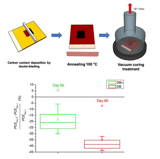
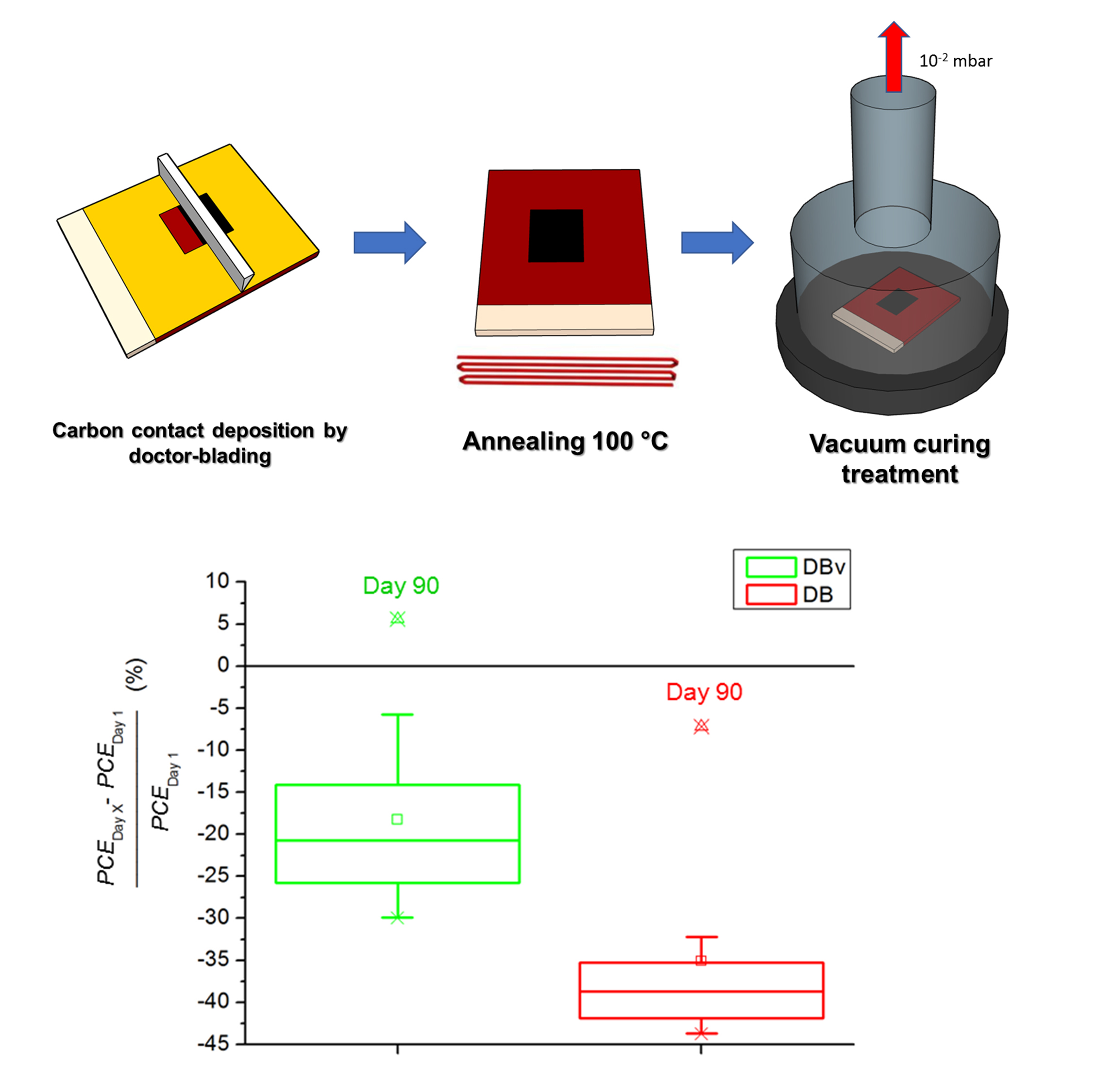
Herein, we investigate a simple fabrication method for the Carbon contact consisting of doctor-blading deposition (
Tannealing = 100 °C) and successive vacuum-curing treatment for 24 h (samples are hereafter called DBv-PSCs). The use of vacuum-curing treatment has been recently reported in the literature for PCBM/Cu selective contacts [
24]. The positive effect on the stability of devices was there associated with a reduction of amorphous regions in the methylammonium lead iodide (MAPbI
3) layer to the benefit of the contact/perovskite interface quality. In our treatment, we apply a mild underpressure of 10
−2 mbar for 24 h on the devices, differently from the work of Ref. [
24], where a long-lasting vacuum treatment was used (100 h) and high vacuum conditions (10
−6 mbar) were needed. As a further difference, we do not remove and then re-deposit the contact layer after vacuum curing, therefore proposing a simplified fabrication procedure. The day-by-day performance comparison with a non-vacuum-treated representative device (DB-PSC), along a timescale of 30 days, shows the positive effect of the vacuum curing treatment on the device stability. The investigation was extended up to 90 days after the device fabrication. Additionally, in order to compare the conditions of the perovskite and its surface under the carbon contact of the DBv-PSC to those of the DB-PSC, X-ray diffraction (XRD) and Conductive atomic force microscopy (CAFM) measurements are performed.
Our approach offers a feasible and simple strategy to fabricate the carbon contact by the doctor-blading method avoiding the typical degradation path of DB-made devices caused by the harmful action over time of the solvent present in commercial C-pastes. Thanks to the vacuum-curing treatment, the preservation of the Carbon/perovskite interface and, consequentially, an improvement of performance stability are achieved.
2. Materials and Methods
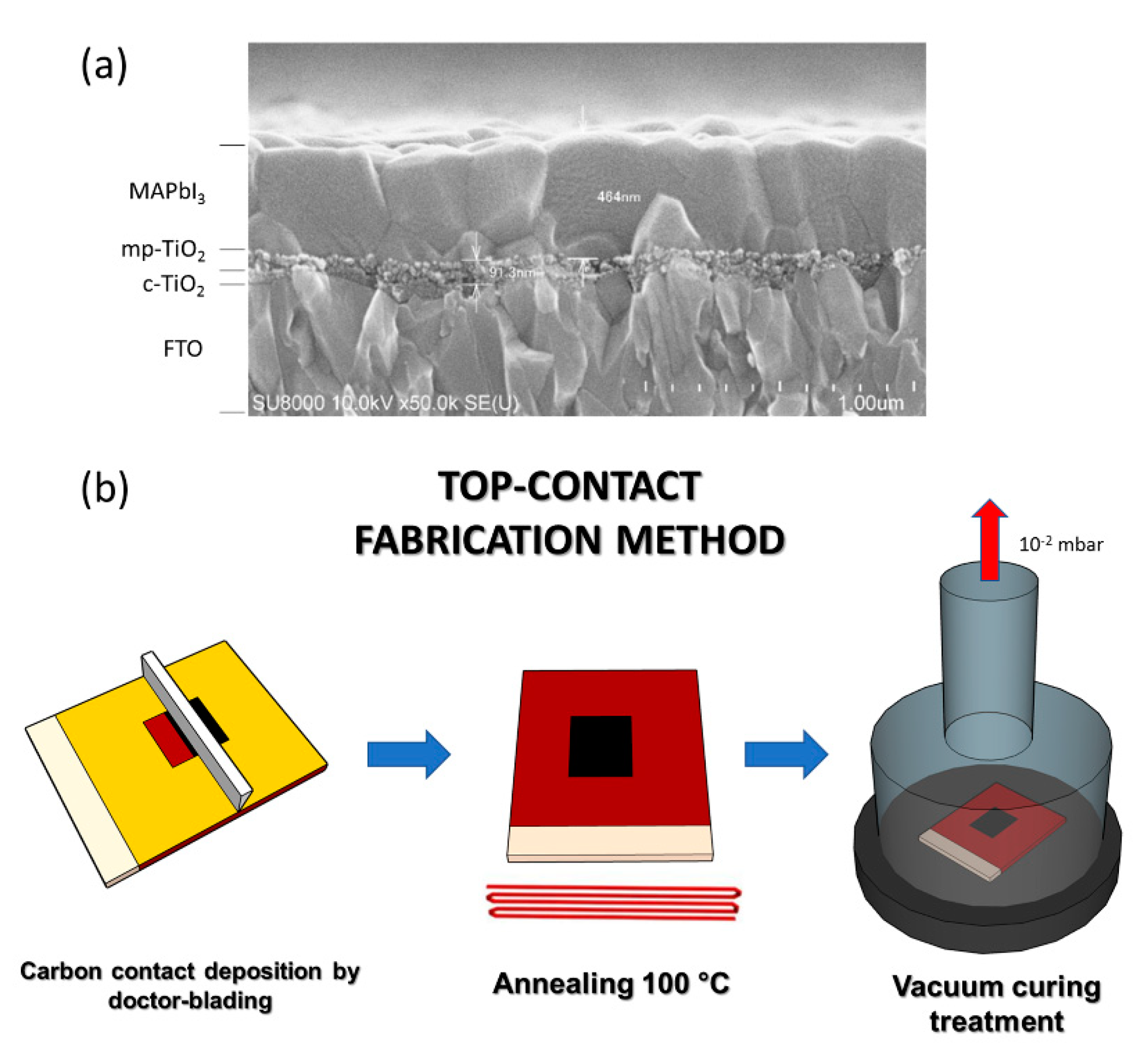
Figure 1a shows a ~450 nm-thick MAPbI
3 layer deposited by solution processing on a ~90 nm-thick meso-porous-TiO
2 (mp-TiO2) on compact-TiO
2 (c-TiO
2)/ fluorine doped tin oxide (FTO). Before preparation of the perovskite film, a perovskite precursor solution and the substrates were warmed at 70 °C. A 1.5 M solution of methylammonium iodide (MAI, 99.0%, Tokyo Chemical Industry, Tokyo, Japan) and lead iodide (PbI
2, 99.99%, trace metals basis, Tokyo Chemical Industry, Tokio, Japan) (1:1 in mol) in N, N-dimethylformamide (DMF) and dimethylsulfoxide (DMSO) (4:1
v/
v) was poured onto the TiO
2 mesoporous substrate and spin-coated (kept for 60 s; 5000 rpm for 30 s with chlorobenzene dripping). The as-prepared film was pot-roast vapor annealing (PR-VA)-treated at 100 °C for 10 min on a hot plate. The resulting perovskite layer was compact and uniform. The size of the grains was in the range of 400–800 nm. Finally, a 30 µm-thick carbon contact (carbon paste DN-CP01 by Dyenamo, Stockholm, Sweden) was deposited on the FTO/c-TiO
2/mp-TiO
2/MAPbI
3 multilayer by the doctor-blading technique and successively annealed at 100 °C for 15 min (DB-PSC). For selected vacuum-treated solar cells (DBv-PSC), we applied 10
−2 mbar for 24 h to the device inside a small vacuum chamber. Both kinds of prepared devices, with and without vacuum-treatment, were taken without encapsulation for the entire experiment. The schematic representation of the preparation process of vacuum-cured perovskite solar cells (DBv-PSCs) is shown in
Figure 1b.
A systematic investigation of the electrical response of representative vacuum cured devices was done by monitoring the performances for 30 days in comparison with reference no-vacuum-treated devices. Measurements were made once per day, acquiring current density-voltage (J-V) characteristics under simulated sunlight.
Table 1 illustrates the operative parameters for solar cell characterization, the aging conditions and the measurements made in order to follow the evolution of device performances during time. The aging conditions are based on International Summit on Organic Photovoltaic Stability-dark storage studies-level 1 (ISOS-D-1) protocol [
25], with the only difference that our cells, after the measurement in air, were kept in nitrogen instead of ambient conditions. That was a precise choice to highlight exclusively the role of the Carbon/perovskite interface without additional effects due toexposure to humidity. The storage in nitrogen environment, in fact, preserves the MAPbI
3 from degradation during storage [
17]. X-ray diffraction analyses were performed after recursive peeling of the carbon contact up to complete removal by an adhesive tape (3M, Saint Paul, Minnesota, USA) in order to explore the entire layer structure and the eventual effect of the vacuum curing treatment. Atomic force microscopy (AFM) was also used to investigate the perovskite surface morphology after carbon contact removal in comparison to the one outside the contact area. Current maps were acquired by conductive atomic force microscopy (CAFM) using a Platinum (Pt) tip to extract a current of holes from the perovskite layer inside and outside the contact regions.
3. Results and Discussion
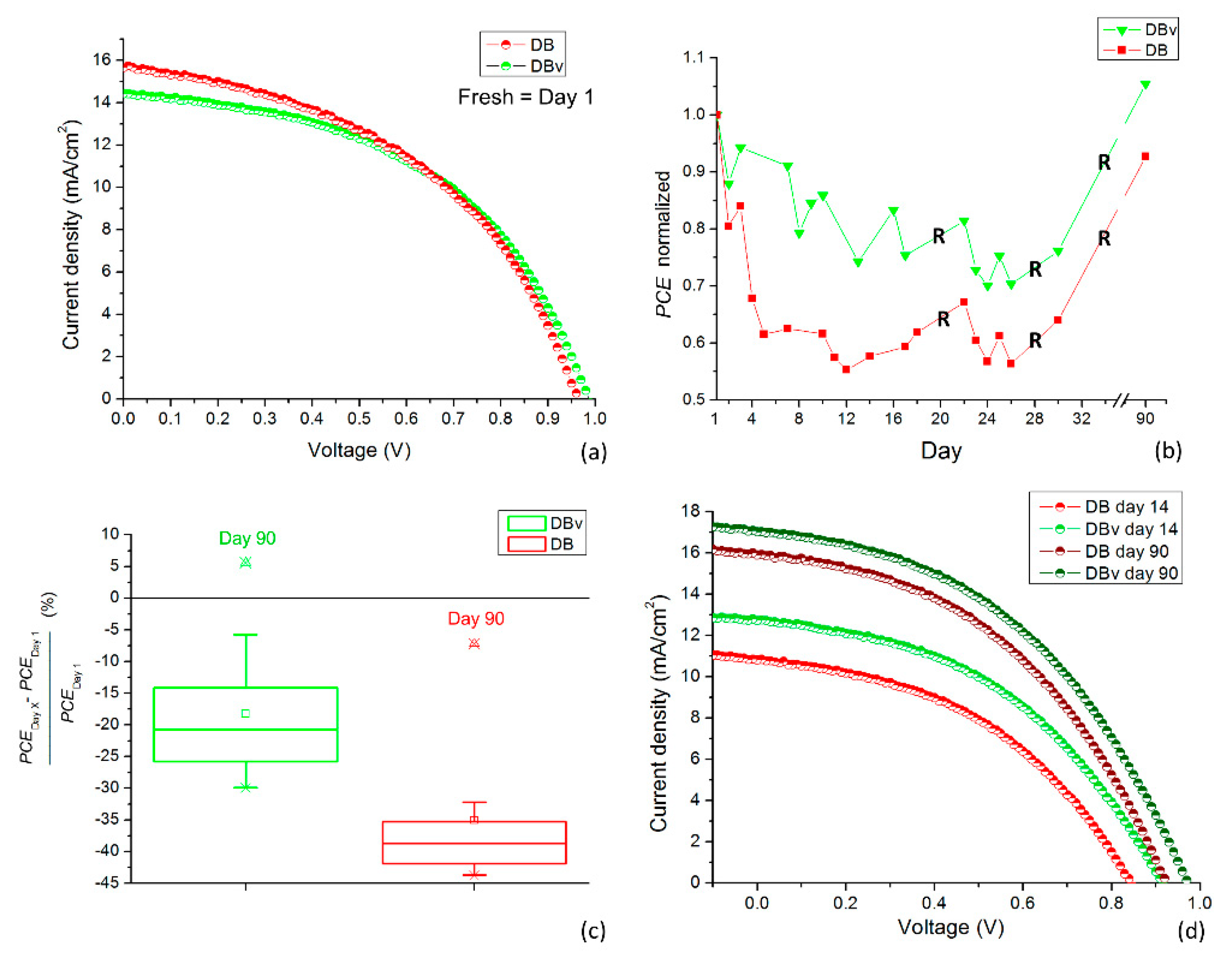
Figure 2a shows the initial performance (day 1) of a representative DBv-PSC compared to a reference device, namely a DB-PSC which was not treated in vacuum after C-deposition. We notice that both devices start working with similar initial power conversion efficiency (
PCE). The DBv-PSC exhibits an efficiency of 6.95% (6.94% for the DB-PSC) with short-circuit photocurrent density (
Jsc) = 14.42 mA/cm
2 (15.65 mA/cm
2 for the DB-PSC), open-circuit voltage (
Voc) = 0.99 V (0.96 V for the DB-PSC), and fill factor (
FF) = 48.7% (46.2% for the DB-PSC), as shown in
Table 2. Such close similarity of the PV parameters, that fall well within the statistics of the single kind of device, indicates that the vacuum treatment does not have any negative effect on the photovoltaic performances.
The temporal trend of the
PCE normalized to the value on day 1 is shown in
Figure 2b. Relative increase or decrease of the
PCE of each device is ascribable to degradation/recovery paths. Here, relative recovery of performances occurring in a time interval ≥4 days of storage in dark and nitrogen environment is marked as “R”.
In general, in the DB-PSC, a short-lasting performance degradation transient was observed, with a 40%
PCE loss with respect to the initial value within ~5 days. From day 5 to day 30, the device shows deterioration/recovery behavior and the
PCE accordingly fluctuates in the range 55–65% of the value on day 1. On the other hand, vacuum curing impacts the long-term stability of the PSC positively, resulting in better efficiency stability over time compared to DB-PSC. In the end, the vacuum-cured PSC indeed loses in average ~20% of the initial
PCE value, as also shown in the box plots in
Figure 2c. This is similar to what we have observed in PSCs with a carbon electrode made by solvent-free hot-press transfer method (HP-PSC) [
23]. Moreover, contrary to the DB-PSC, the DBv-PSC does not show the degradation transient behavior in the first days. Since day 1, it exhibits the degradation/recovery pathways similarly to what happens for HP-PSC [
23].
On day 30, both kinds of devices were stored in dark conditions, with no bias applied and in a nitrogen environment. After 60 days of storage, both DB-PSC and DBv-PSC were measured to evaluate their “aged” performances. It is noteworthy that both cells have instead recovered their performances in comparison with the last run of measurements. A similar effect is reported in our previous work wherein the top contacts were made without HTL, with the maximum gain achieved by avoiding solvent-perovskite interaction during contact fabrication [
23]. In this regard, doctor-blading compared to the hot-press transfer method provides a better guarantee of adhesion to the underlying perovskite through the whole contact area and it is thus believed to be technologically more reliable.
Furthermore, as shown in
Figure 2b, the performances of the DBv-PSC on day 90 are even better than those on day 1, with an increase of the
PCE value by ~6% (7.34% vs. 6.95%), as opposite to what happens to the DB-PSC (decrease of
PCE values by ~6%).
Figure 2c shows the distributions of percent variations of
PCE from day 1 up to day 90, displayed as box-plots, with respect to the value on day 1 for the DB-PSC and the DBv-PSC. The average values, represented by the horizontal lines in the figure, are −20% and −40% for the DBv-PSC and the DB-PSC, respectively, indicating a minor loss of performances for vacuum-treated devices. The values recorded in the DBv-PSC are more widely scattered than those of the DB-PSC, resulting in a larger box. This is due to better efficiency recovery in the DBv-PSC case. Finally, the outliers in
Figure 2c present the
PCE percent variations after 60 days of storage/measured on day 90. The DBv-PSC shows a surprising
PCE increase by ~6% (value higher than the zero line) as opposite to the DB-PSC (about −6%).
Figure 2d compares the J-V curves of the two kinds of devices on day 14 (worst condition) and day 90 (final condition).
Table 2 summarizes the values of photovoltaic parameters (open circuit voltage, short current density, fill factor and
PCE) for both DB-PSC and DBv-PSC on day 1, day 14, and day 90. A huge improvement of all photovoltaic parameters is observed on day 90 (after 60 days of storage in dark conditions with no bias applied and in nitrogen environment) compared to values on day 14.The increase in
Jsc of the vacuum-treated device is especially noteworthy (
Figure 2a).
The observed electrical phenomenon likely arises from improved perovskite lattice structure that could also involve the interface with the contacting material. However, the extra-gain introduced by the vacuum treatment indicates that the self-healing of the perovskite core [
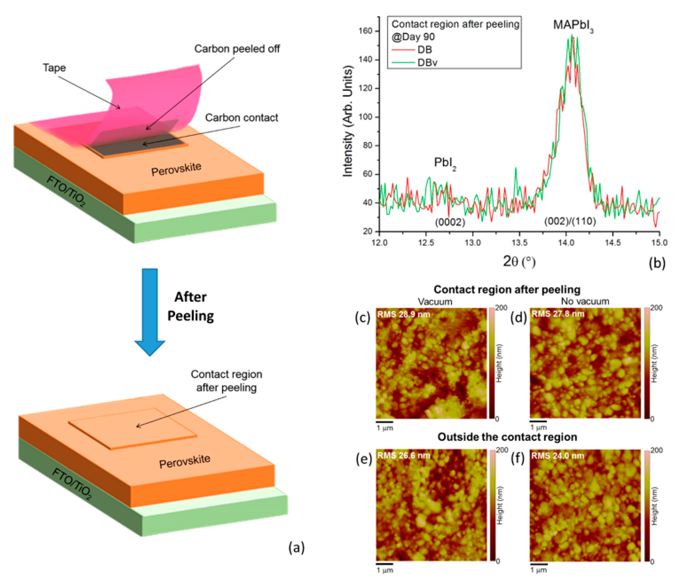
26], which would occur in both kinds of device, is not an exhaustive explanation. To understand the origin, the Carbon contacts were removed by a process of progressive peeling using a sticky tape (
Figure 3a) on day 90 after the last J-V measurements. The structural, morphological and electrical changes of the exposed MAPbI
3 surface were analyzed. The composition inside the contact regions was unfolded by X-ray diffraction, as shown in
Figure 3b. The measurements reveal the same amount of MAPbI
3 (main peak at 2θ = 14.1°) and almost negligible traces of PbI
2 (main peak at 2θ = 12.7°) in both kinds of devices, suggesting no irreversible macroscopic degradation in the perovskite layer under the carbon contact. Our finding indeed moves the focus towards the carbon/perovskite interface. This interface could be pivotal in improving the stabilty of the device, in agreement with the recent literature on other cell architectures [
6,
27,
28].
We have thus investigated the morphology of the MAPbI
3 surface by atomic force microscopy (AFM) measurements in different regions, namely inside and outside the contact area after peeling. The morphological analyses on representative devices show negligible differences between the DBv-PSC and the DB-PSC (
Figure 3c–f) in both regions, with no evident changes in grain size and roughness. On this basis, we conclude that no significant morphological changes have occurred after deposition of the carbon contact by the doctor-blading method, during vacuum curing and after the contact peeling.
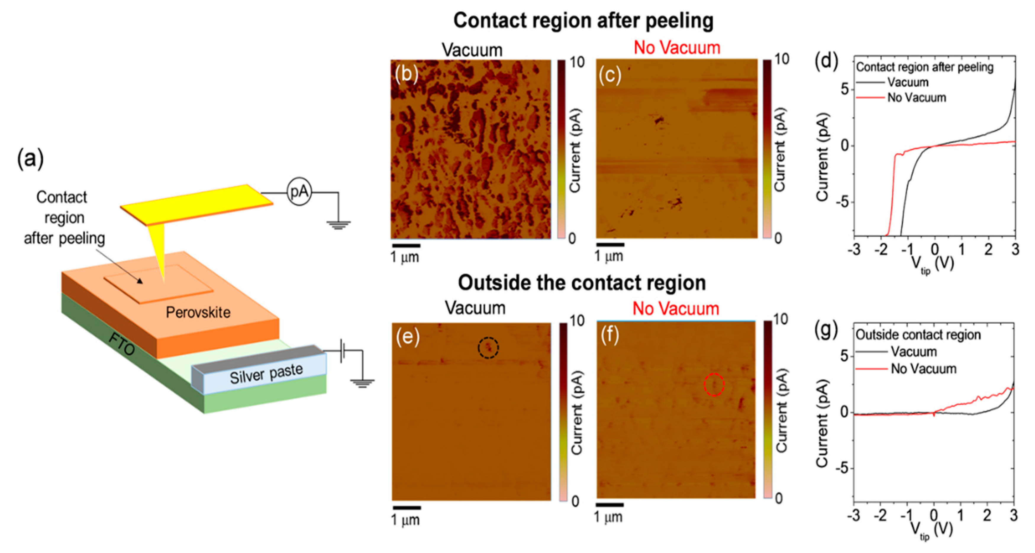
Surface morphology and electrical behavior are not necessarily correlated. To go deeper into the process of carrier extraction from the perovskite surface, local electrical analyses using conductive atomic force microscopy (CAFM) were performed. CAFM was applied to explore the electrical behavior of the MAPbI
3 surface at the nanometre scale both inside and outside the contact region after peeling. Local current mapping of MAPbI
3 surfaces, as illustrated in
Figure 4a, was collected by CAFM using a Pt-coated Silicon tip. By applying a positive bias to the electrode, holes are extracted owing to a proper band position of Pt with respect to MAPbI
3. All the measurements have been performed under dark conditions.
From the CAFM maps, it is clear that higher currents flow-out through the Pt-tip in the contact region of the DBv-PSC (
Figure 4b) while the DB-PSC (
Figure 4c) counterpart shows low current flow. The more efficient hole extraction from the perovskite surface inside the contact region (after C-contact peeling) in vacuum-treated devices is confirmed by the local I-V measurements shown in
Figure 4d. From the shape of the electrical curve, we notice that the rectifying behavior of the tip-perovskite interface and the higher collected current at a fixed voltage in the forward scan (V > 0), compared to the reference DB-PSC. Both devices in the area outside the peeled C-contact region exhibit similar electrical response and are less performing than the perovskite surface after peeling in the vacuum-treated devices.
The positive role of the vacuum treatment was indeed clearly stated by the improved quality of the perovskite surface under the C-contact to release holes. We argue this effect to be partially linked to a positive action of the vacuum to further remove residual solvent from the contact after doctor-blading deposition. This is in agreement with the findings of our previous publication, wherein the solvent was prevented to interact with the perovskite layer by applying a hot-press method [
23]. Additional positive effects linked to carbon interacting and stabilizing the perovskite surface through modifications at the atomic scale cannot be excluded.

 ,
, 


