1. Introduction
An integrated lens antenna (ILA) is an antenna composed of a feed and lens structure that has the characteristics of high gain and a narrow beam. It has many applications in imaging [
1], communications [
2], radar [
3], and other fields. It converts the spherical surface emitted by the feed into a plane wavefront, thus improving the antenna’s directivity [
4]. Traditional lens shapes are elliptical, hemi-spherical, or extended hemispherical, and their principles are usually similar to collimate electromagnetic waves, that is, from the perspective of geometric optics [
5]. In recent years, Fresnel lenses [
6] and meta-material lenses [
7] have also been released. The shape of these lenses can reduce the cross-section of the lens, but the feed needs to be a certain distance from the lens and will also occupy a specific size. The lens material is usually made of low-loss-Tangent (D
f), low-dielectric-constant (D
k) materials, such as polyethlyene [
8] (D
k = 2.3, D
f = 0.0005) and polystyrene [
9] (Dk = 2.5, D
f = 0.0002). They have the advantages of low cost and easy processing. However, their mechanical strength and heat resistance need to be improved. Quartz material is another lens option. It also has a relatively low dielectric constant and low loss (D
k = 3.75, D
f = 0.0002) [
10]. A disadvantage is that the cost increases compared to organic materials such as polyethene. Silicon (D
k = 11.9, D
f = 0.01) is also used as a lens material in high-frequency bands, such as millimeter wave and sub-terahertz, because the size of the antenna in this frequency band will be reduced to the micron level [
11]. The feeds that require integrated lenses include waveguides [
12], horns [
13], and microstrips [
14]. Since waveguides and horns have no media loss, they can transport more energy into the lens, generating radiation. However, integrating into other products is more extensive and more challenging. In contrast, the microstrip antenna has a dielectric substrate to facilitate integration with the circuit. However, it has a specific dielectric loss, and its directivity could be better than the others. The substrate material of a microstrip antenna is usually made of printed circuit board (PCB), such as Rogers 5880 [
15]. It has excellent dielectric properties and is widely used as the substrate material of planar antennas. Glass has also recently been used as a substrate material due to its high mechanical stability and excellent radio frequency performance. Some works have used glass substrates for radio frequency packaging research and antenna application demonstrations [
16]. In the millimeter-wave frequency band, glass substrates have significant advantages because the error of metal lines prepared by the micromachining process is much smaller than that of the PCB line preparation process.
Lenses with complex structures have also been proposed. For example, in situations where beam scanning is required, traditional dielectric lenses lose their advantages. N. T. Nguyen et al. used Ultem (D
k = 3.01, D
f = 0.003) materials to prepare dual lenses, reducing the lens antenna’s scanning loss [
17]. S. K. Karki et al. prepared a metallic dielectric lens (IMLA) from polyethene and stainless steel, reducing scanning loss [
18].
For scenarios that do not require beam scanning, some works focused on improving the size and peak gain of the lens in recent years. B. T. Malik et al. [
19] used 3D printing technology to prepare a hollow hemispherical lens with a 50% air ratio, which reduced the dielectric loss of the lens and increased the gain. Lee et al. [
20] prepared a double-sided lens from polyethene, reducing the equivalent gain lens size by 31%. Abdallah Dhouibi et al. [
21] used flat metal materials to prepare a Luneburg lens with metamaterial properties, achieving a gradient refractive index and reducing the antenna profile and aperture. However, the structure of the antenna mentioned above is relatively complex and requires complex preparation processes. Some scholars have proposed that in a microstrip-fed hemispherical lens antenna, the excitation of surface waves can be suppressed when the dielectric constants of the substrate and the lens are similar, but more research needs to be undertaken [
22]. This study presents the design of an integrated lens antenna, where both the substrate and lens are composed of quartz material. Through simulation and empirical measurements, it is demonstrated that the antenna effectively minimizes the lateral surface electric field and mitigates the impact of surface waves. A lens antenna on a PCB substrate was designed and prepared as a control.
Furthermore, the authors designed a PCB-substrate quartz lens antenna for comparative analysis. The operational mechanism of this lens antenna configuration is elucidated.
Section 2 outlines the objectives and criteria for the lens antenna, as well as the preparation and assembly processes involved.
Section 3 describes the electric-field mechanism that takes place when the lens antenna operates and the principle of enhancing the antenna gain by suppressing surface waves. Moreover, the actual measurement and simulation results demonstrate this. Finally, the conclusions of this paper are presented in
Section 4.
2. Design and Fabrication
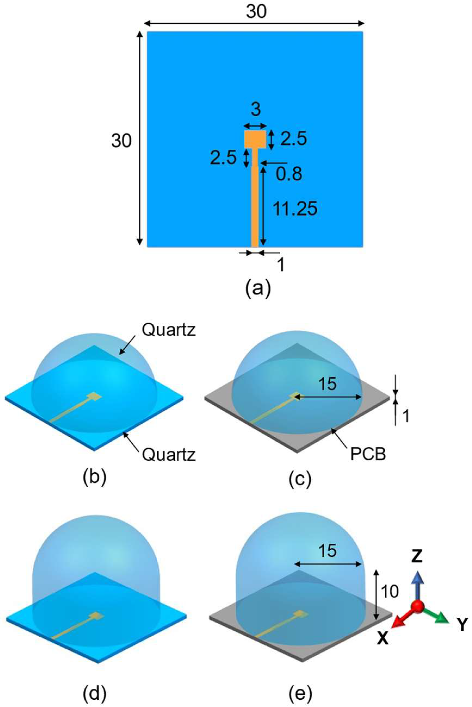
Two integrated quartz lens antennas (D
k = 3.75 and D
f = 0.0002) are proposed, along with two comparative quartz lens antennas fabricated on PCB substrates (D
k = 2.2 and D
f = 0.001). The microstrip antenna under the lens and the size of each part are shown in
Figure 1a.
Figure 1b shows the configuration of the quartz-substrate hemispherical lens. The PCB-substrate quartz hemispherical lens is shown in
Figure 1c. The quartz-substrate extended hemispherical lens is shown in
Figure 1d. The PCB-substrate extended hemispheric lens is shown in
Figure 1e. To facilitate analysis, the PCB antenna only changes the material of the substrate, and the size of the patch and the size and material of the lens remain unchanged.
The integrated lens antenna design process involves the following key steps: (1) Initially, the length and width of the patch, as well as the size of the feeder, must be determined based on the thickness of the dielectric substrate, the center frequency, and the impedance matching. (2) The lens is then added. When a lens is placed directly above the designed microstrip antenna, it causes changes in the impedance and frequency characteristics of the antenna. In this case, adjustments to the size of the feeder and patch are required to optimize the antenna for the target frequency band and to achieve a favorable radiation pattern. (3) During the design of the extended lens, the height of the cylindrical structure must also be optimized. An ideal height is initially set, followed by the optimization of the patch size. Finally, the height of the cylinder is adjusted accordingly. If the height is not properly chosen, radiation pattern distortion may occur, leading to a defocused beam.
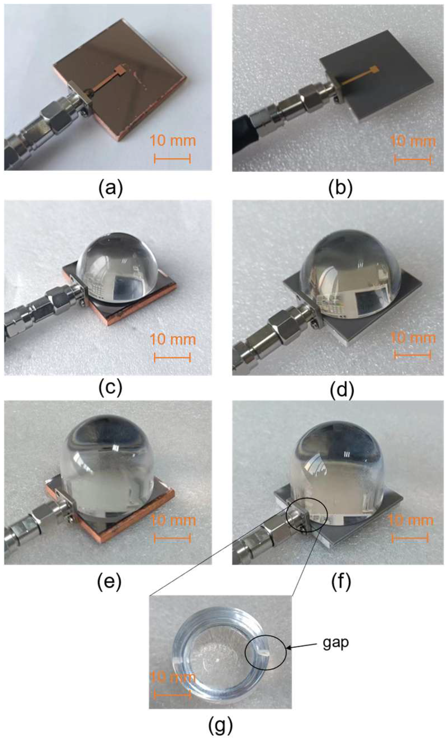
The microstrip antenna is fabricated on a quartz substrate using micromachining technology. A 1 mm thick quartz substrate is initially prepared, followed by the spin-coating of 6 μm of 4620 photo-resist on the front side, which is then photoetched. Then, 20/3000 nm Ti/Cu films are subsequently sputtered onto both sides of the substrate. The substrate undergoes an acetone immersion process for several hours to facilitate the peeling operation. The PCB substrate is fabricated using a standard process, with a Cu layer thickness ranging from 20 to 30 μm. Hemispherical and extended hemispherical quartz lenses are prepared through mechanical processing.
Figure 2 depicts all the assembled integrated lens antennas with a Sub-Miniature version A (SMA) connector.
It is worth noting that since the area of the lens we designed is the same as the substrate, this affects the connection between the feeder and the SMA connector. Therefore, during actual operation, part of the side of the lens is ground off to install the SMA connector, as shown in
Figure 2g.
3. Results and Discussion
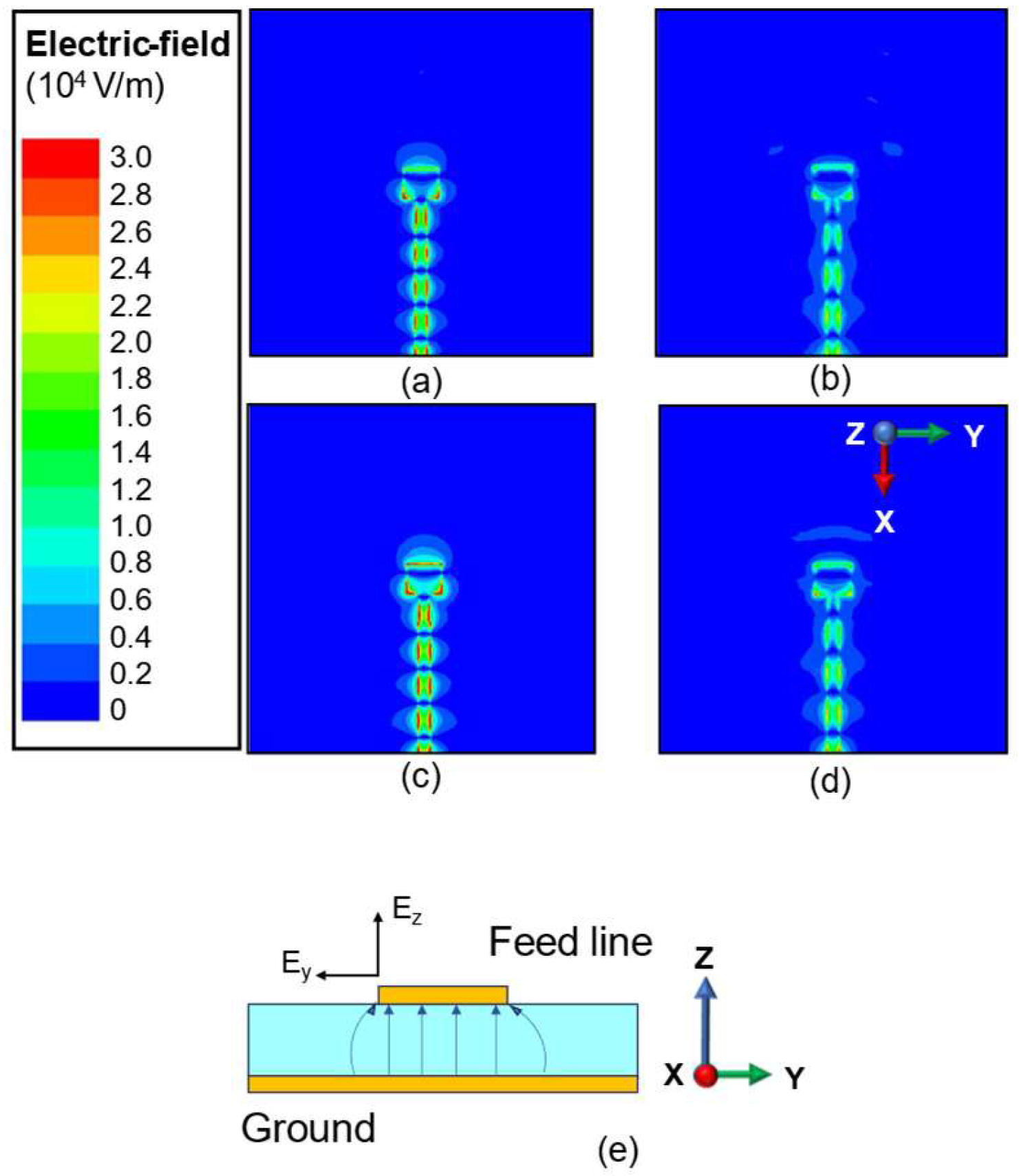
This section uses Ansys HFSS 2021 R1 (Canonsburg, PA, USA) software to analyze the electric field.
Figure 3 describes the electric-field distribution on the upper surface of the microstrip antenna. The electric field intensity of the four images has a minimum value of 0 V/m and a maximum value of 3 × 10
4 V/m. The electric field distribution of the quartz-substrate hemispherical lens antenna is shown in
Figure 3a. The electric-field distribution of the PCB-substrate hemispherical lens antenna is presented in
Figure 3b. The electric-field distribution of the quartz-substrate extended hemispherical lens is shown in
Figure 3c. The electric-field distribution of the PCB-substrate extended hemispherical lens is presented in
Figure 3d. By electric-field analysis, it is found that the electric field of the quartz-substrate antenna is more concentrated than that of the PCB-substrate antenna. The electric field is focused on the metal patch, with a small amount of scattering around the periphery. The electric-field intensity on the PCB antenna metal patch is comparatively lower, while the surrounding electric field exhibits a more pronounced intensity. The propagation direction of the electromagnetic waves is along the negative X-axis. At the edge of the microstrip line, the electric field can be decomposed into E
z and E
y, as shown in
Figure 3e. The E
z of the quartz-substrate antenna is higher than that of the PCB-substrate antenna, whereas the E
y of the quartz-substrate antenna is lower than that of the PCB-substrate antenna. The reduction in E
y in the quartz-substrate antenna weakens the surface wave loss, which in turn enhances the radiation efficiency and gain of the antenna. This phenomenon suggests that the presence of surface waves diminishes the antenna gain along the Z-axis. At the feed line of the quartz substrate, there are approximately 4.5 half-wavelengths of electromagnetic waves, as shown in
Figure 3a,c, while the feed line of the PCB substrate exhibits about 4 half-wavelengths, as presented in
Figure 3b,d. This difference arises from the higher dielectric constant of quartz (Dk = 3.75) compared to PCB (Dk = 2.2), which results in a shorter equivalent wavelength for the transmission line on the quartz substrate. At this time, the electromagnetic waves form a standing wave state on the transmission line.
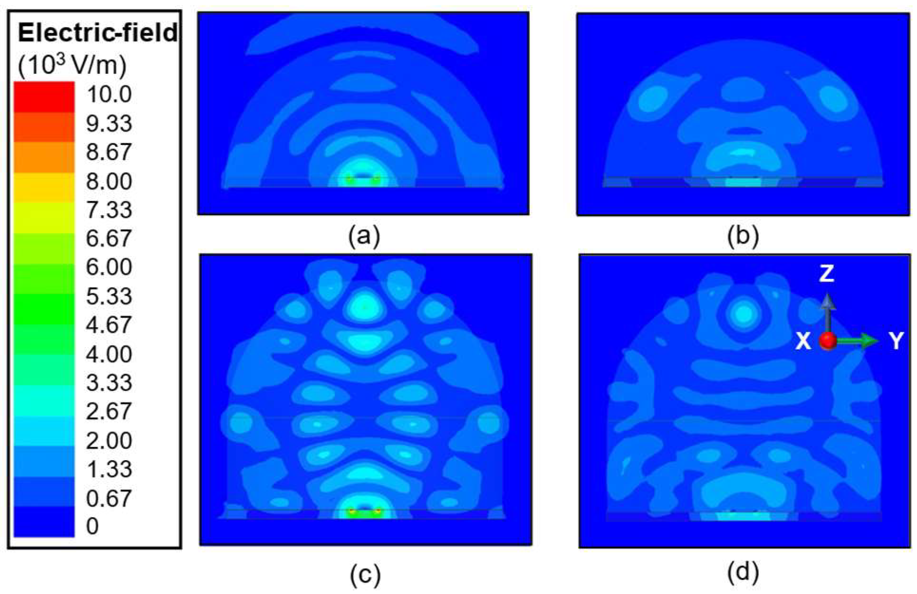
Figure 4 shows the electric-field distribution in the YOZ plane of the ILA. The maximum is 1 × 10
4 V/m and the minimum is 0. The electric-field distribution of the quartz-substrate hemispheric lens is presented in
Figure 4a. The electric-field distribution of the PCB-substrate hemispheric lens is presented in
Figure 4b.
Figure 4c shows the electric-field distribution of the quartz-substrate extended hemispherical lens.
Figure 4d depicts the electric-field distribution of the PCB-substrate extended hemispherical lens. The electric field of the quartz-substrate lens antenna is concentrated on the middle metal patch, and the lens part has a small amount of electric-field intensity. Although the electric field of the PCB substrate is also concentrated on the middle metal patch, the electric-field intensity suddenly changes at both ends of the dielectric interface; that is, the electric-field intensity is discontinuous.
To facilitate the analysis of the radiation characteristics, the authors expanded the simulation area and observed the far-field electric-field behavior of the lens antenna. The upper and lower limits of the electric field strength are 0.1 × 10
3 V/m, respectively.
Figure 5a shows the electric-field distribution of the comparative microstrip antenna. The electric field radiates a quasi-spherical wavefront uniformly along the average direction of the antenna. This wavefront gradually attenuates with the distance it propagates.
Figure 5b,c describes the electric-field distribution characteristics of the quartz substrate hemispheric lens and the PCB substrate hemispheric lens. When the hemispheric lens is installed, the electromagnetic wavefront does not change significantly and is still a quasi-spherical wave. It can be inferred that the antenna directivity of the hemispheric lens is not significantly improved. However, the PCB substrate reflects more inside the lens than the quartz substrate, causing the lateral component of the electric field to increase and the energy response radiated in the expected direction to weaken.
Figure 5d,e depicts the electric-field characteristics of the quartz-substrate extended hemispheric lens antenna and the PCB-substrate extended hemispheric lens antenna. Adding an extended hemispherical lens after the electromagnetic wave is reflected and focused inside the lens converts it from a quasi-spheric into a plane wavefront. The plane wavefront exhibits higher directivity, with a reduction in propagation attenuation as the distance increases. Upon the installation of an extension lens, the antenna beam is further collimated, resulting in enhanced directivity and an improved normal gain response. In addition, the electric-field intensity in the average direction of the quartz-substrate antenna is higher than that of the PCB-substrate antenna. This is also caused by the different materials of the substrate and lens, which causes more reflections, more lateral energy, and weakened average energy. Placing a hemispherical lens at an optimal distance from the surface of a microstrip antenna can shape the radiated energy to resemble a plane wavefront, thereby enhancing the gain. However, if the lens is positioned too close to the antenna substrate, the radiated wave will tend toward a spherical wavefront, resulting in a loss of focus and a reduction in the gain along the Z-axis.
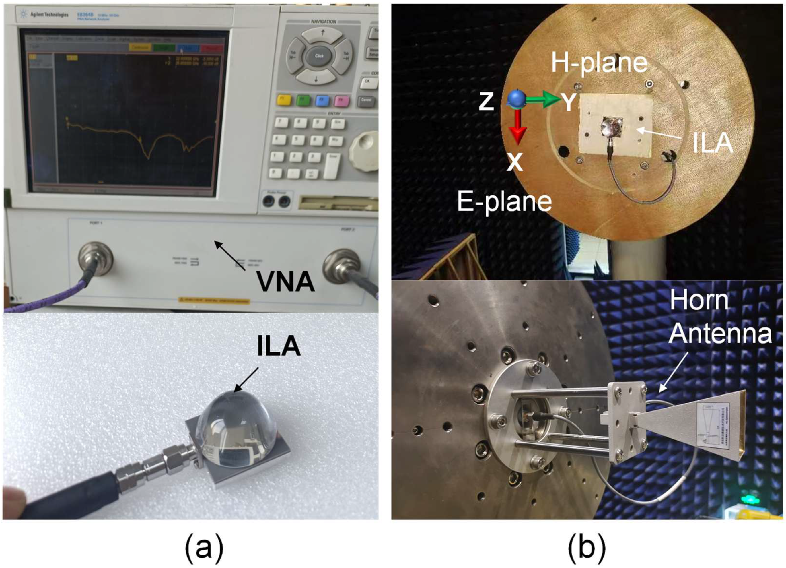
Figure 6a shows the measurement setup of the ILA, with the Vector Network Analyzer (VNA) and the ILA sample connected to the connector.
Figure 6b presents the measurement setup in the darkroom. One side is a lens antenna and the other is a standard horn antenna.
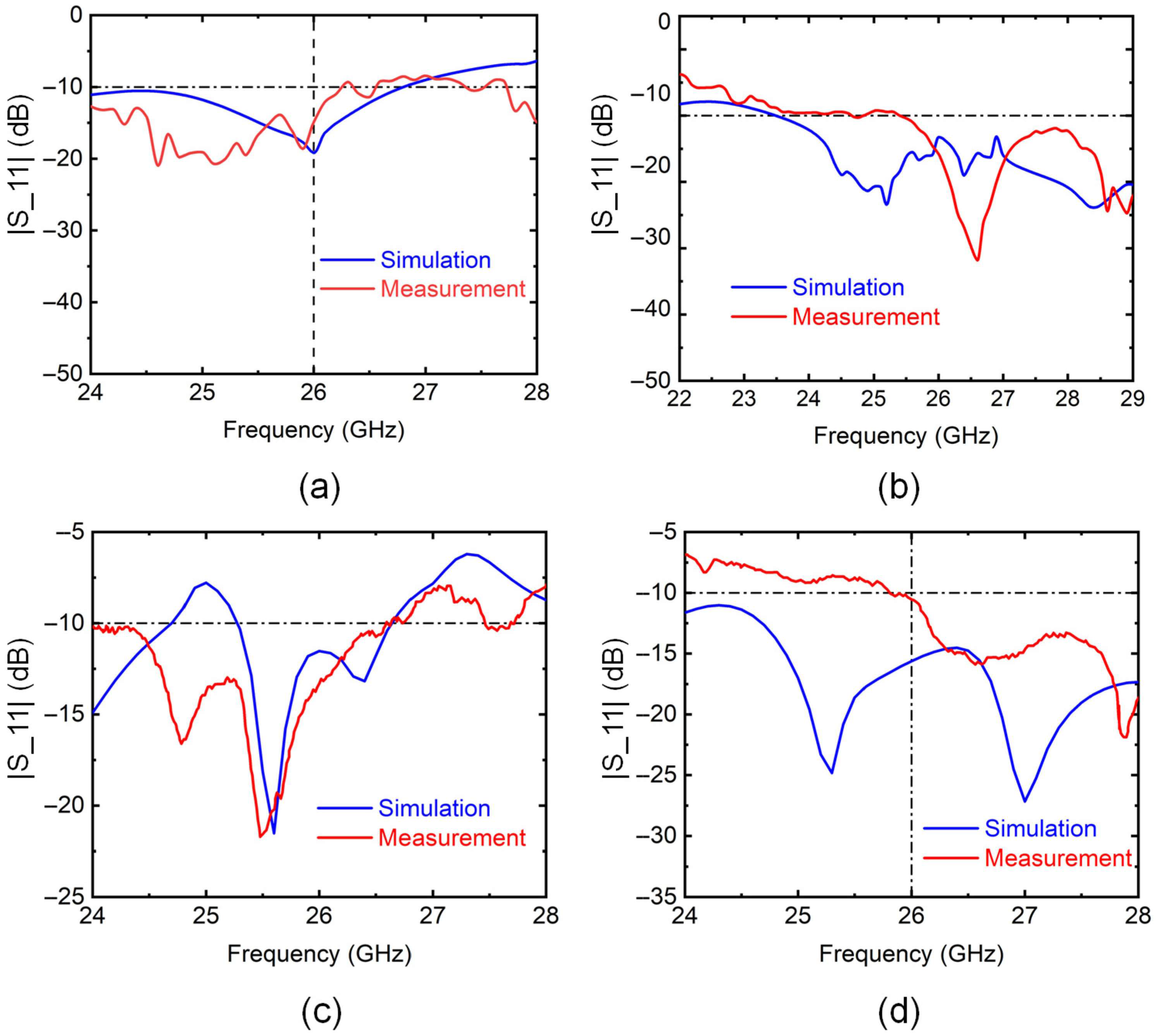
Figure 7a shows the |S_11| simulated and measured value of the quartz-substrate hemispheric lens.
Figure 7b illustrates the |S_11| simulated and measured value of the PCB-substrate hemispheric lens.
Figure 7c describes the |S_11| value of the quartz-substrate extended hemispheric lens.
Figure 7d depicts the |S_11| value of the PCB-substrate extended hemispheric lens. The quartz-substrate microstrip antenna is designed for operation at a frequency of 26 GHz. However, when the substrate material is substituted with PCB, a change in the impedance of the antenna occurs. This alteration in impedance results in a variation in |S_11|. Despite these changes, both antenna configurations meet the performance requirements at the 26 GHz operating frequency. The discrepancy between the actual measurements and the simulation results can be attributed to errors inherent in the machining of the quartz lens, as well as deviations arising during the bonding process of the quartz to the substrate.
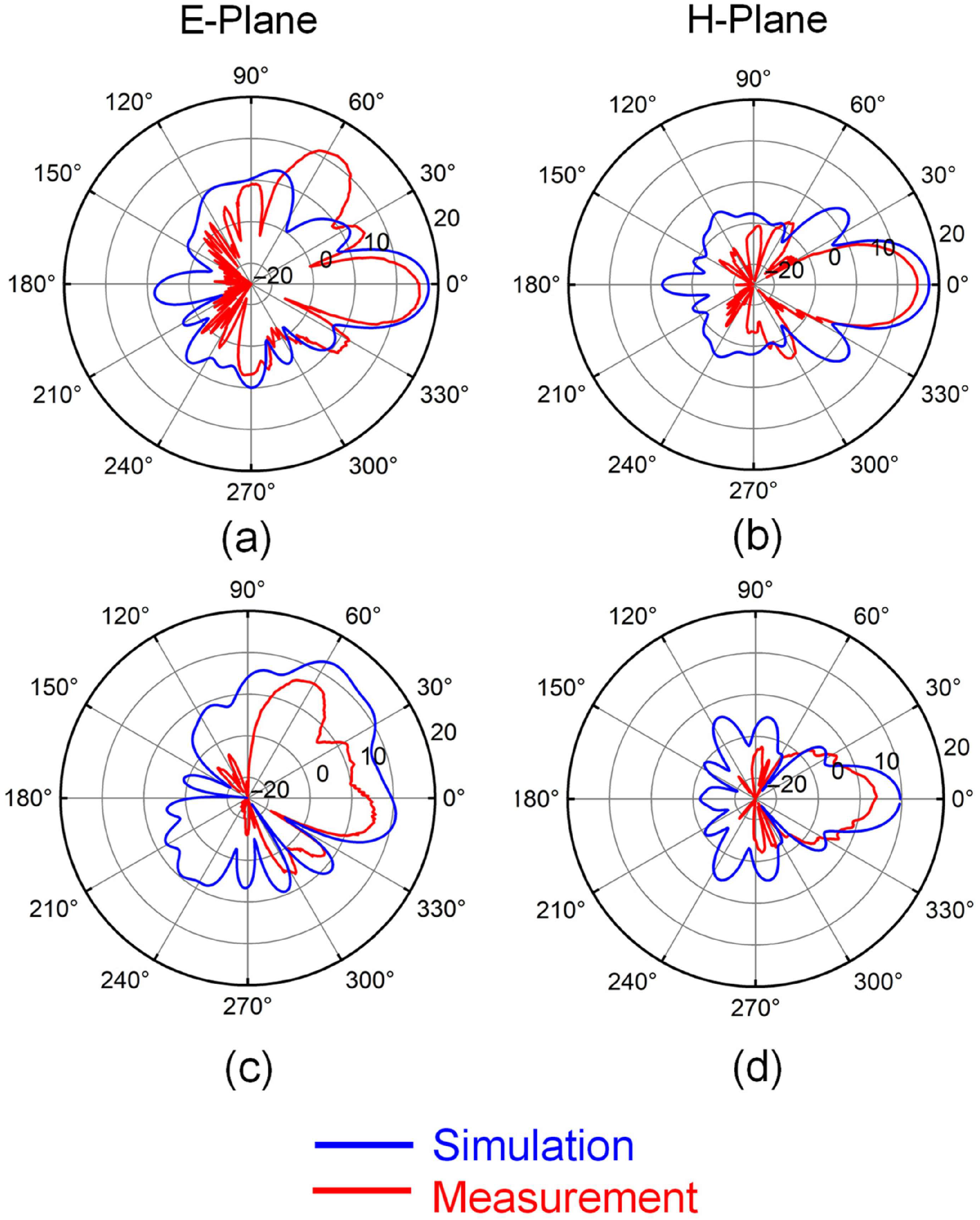
Figure 8a shows the E-Plane radiation pattern of the quartz-substrate hemispheric lens.
Figure 8b describes the H-plane radiation pattern of the quartz-substrate hemispheric lens.
Figure 8c depicts the E-plane radiation pattern of the PCB-substrate hemispheric lens.
Figure 8d presents the H-Plane pattern of the PCB-substrate hemispherical lens. The peak gain of the quartz-substrate hemispherical lens antenna is on the Z-axis. However, the E-Plane main lobe of the PCB-substrate hemispheric lens decreases and the side lobe increases. The gain of the Z-axis is significantly lower than that of the quartz substrate, from 8.54 dBi to 6.16 dBi. This is due to the presence of surface waves in the PCB substrate, which increases the number of miscellaneous modes in the antenna, causing the side lobes of the radiation pattern to rise and the gain of the main lobe to decrease. This is consistent with the results of the analysis of the abovementioned electric-field distribution. The electric field is concentrated on the metal patch, and the far-field radiation pattern of the antenna will have a concentrated main lobe and fewer side lobes. If the electric-field intensity on the antenna surface is dispersed, the side lobes of the far-field pattern will increase, and the gain of the main lobe will decrease. The measured gain value is slightly reduced, but the radiation pattern is consistent with the simulated value. This may be related to a machining error in the quartz lens. The substrate inside the lens processed this time needs to be uniform enough, resulting in certain deviations in the propagation path of the electromagnetic waves.
Figure 9a describes the E-Plane radiation pattern of the quartz-substrate extended hemispheric lens.
Figure 9b shows the H-Plane radiation pattern of the quartz-substrate extended hemispheric lens.
Figure 9c presents the E-Plane radiation pattern of the PCB-substrate extended hemispheric lens.
Figure 9d illustrates the H-Plane radiation pattern of the PCB-substrate extended hemispheric lens. According to the simulation results, the peak gain of the quartz-based extended lens antenna is on the Z-axis, and the peak gain is 17.68 dBi. The measured peak gain of the quartz-substrate hemispheric lens on the E-Plane is 15.49 dBi, and the peak gain on the H-Plane is 14.93 dBi, slightly lower than the simulated value. In addition, the side lobes near the main lobe also decrease slightly. The gain of the measured value around 180° decreases; that is, the front-to-back ratio of the measured antenna increases. This is because the substrate and metal materials in the measured scene lose part of their energy, reducing the received energy of the horn antenna. The measured and simulated results exhibit a high degree of consistency. The maximum average gain of the PCB-substrate extended lens antenna is limited to 10 dBi. However, the peak gain of the extended lens antenna surpasses that of the hemispherical lens. This can be attributed to the principle of geometric optics, which dictates that the convex surface of the hemispherical lens is positioned at a certain distance from the microstrip antenna. This separation allows the electromagnetic wave to propagate through the lens, undergo focusing, and subsequently radiate. This process aids in converting the spherical wavefront into an approximate planar wavefront, thereby enhancing the antenna’s radiation performance. The energy of the plane wavefront is more concentrated, which increases the antenna’s gain. In addition, it can also be seen that the side lobe of the PCB-substrate extended hemispherical lens is also more extensive than that of the quartz-substrate lens, and the corresponding main lobe gain is reduced. This is also due to surface waves; the electric field on the substrate surface has a specific transverse direction.
Table 1 presents a summary of related works from recent years. The antenna proposed in this paper is capable of maintaining both a compact size and high gain.


