
A Survey of Machine and Deep Learning Techniques in Analog Integrated Circuit Layout Synthesis


Abstract
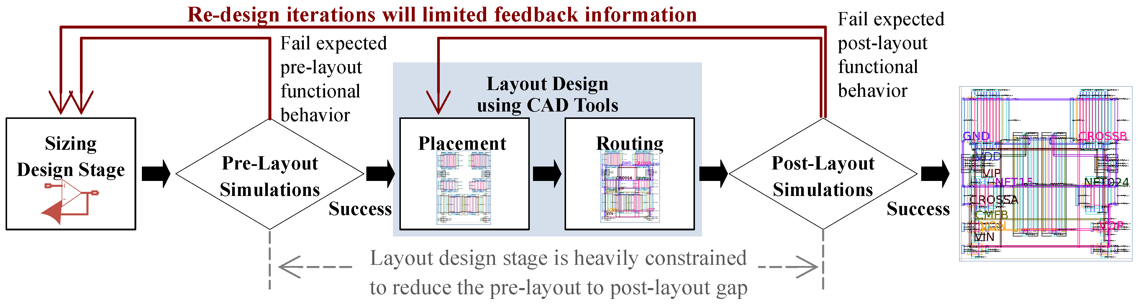
1. Introduction
2. Placement
2.1. A Summary of Traditional Automatic Approaches
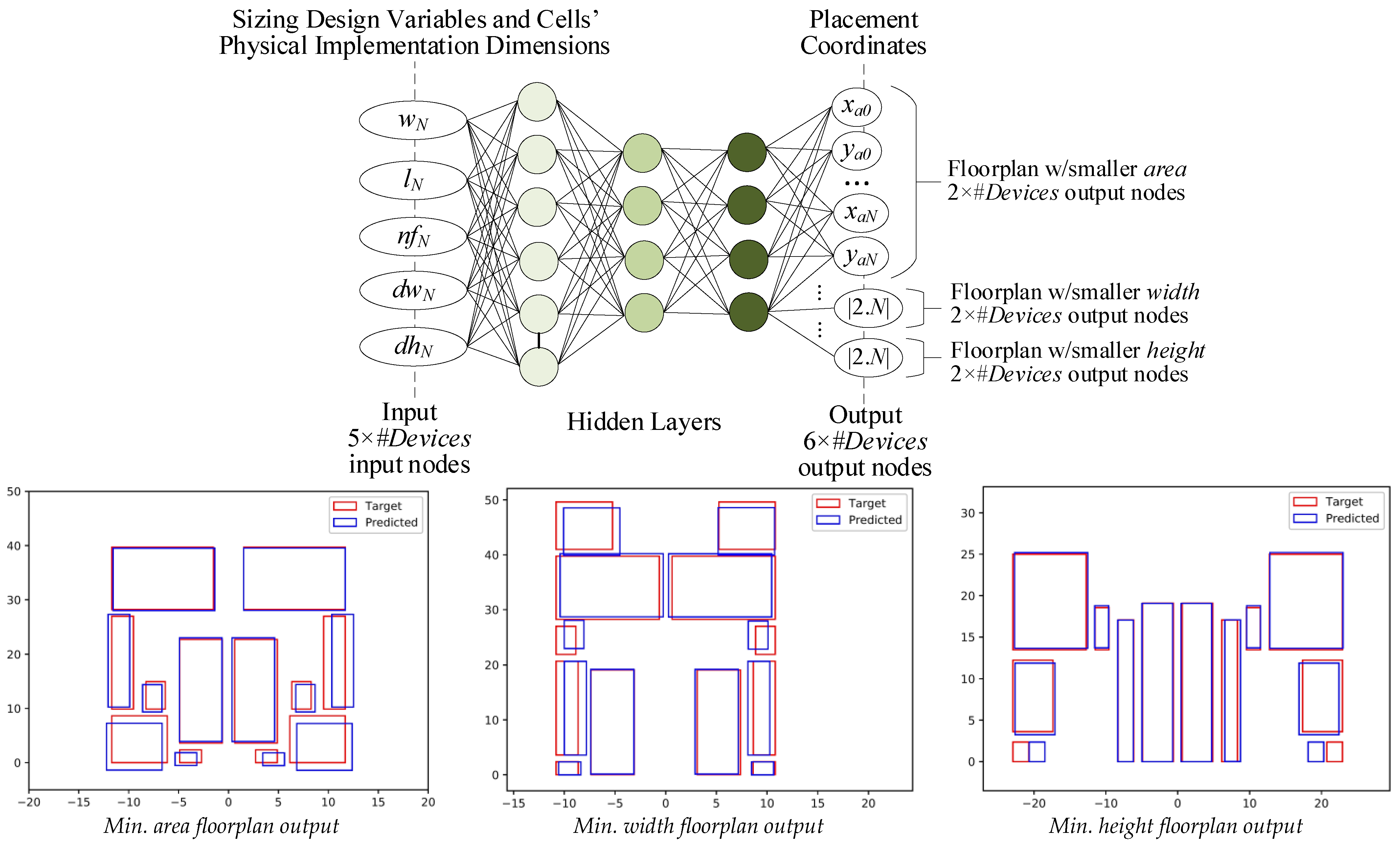
2.2. M/DL Advances: Neural Network-Based
2.3. M/DL Advances: Reinforcement Learning-Based
3. Routing
3.1. A Summary of Traditional Automatic Approaches
3.2. M/DL Advances
4. Post-Layout Performance Prediction
4.1. Traditional Performance-Driven Layout Generation Tools
4.2. Direct Transfer Learning from Pre- to Post-Layout
4.3. M/DL Advances: Classification-Based Approaches
4.4. M/DL Advances: Regression-Based Approaches
5. Discussion and Future Research Directions
6. Conclusions
Funding
Conflicts of Interest
Abbreviations
| AI | Artificial Intelligence |
| ANN | Artificial Neural Network |
| B*-Tree | Binary Tree |
| BO | Bayesian Optimization |
| CAD | Computer-Aided Design |
| CNN | Convolutional Neural Network |
| DL | Deep Learning |
| EBL | Electron-Beam Lithography |
| EDA | Electronic Design Automation |
| GAN | Generative Adversarial Network |
| IC | Integrated Circuit |
| LDE | Layout-Dependent Effect |
| MDP | Markov Decision Process |
| M/DL | Machine and Deep Learning |
| MLP | Multi-Layer Perceptron |
| O-tree | Ordered Tree |
| PDK | Process Design Kit |
| PM | Phase Margin |
| R-GCN | Relational Graph Convolutional Neural Network |
| RL | Reinforcement Learning |
| SA | Simulated Annealing |
| SoC | System-on-a-Chip |
| SP | Sequence Pair |
| TCG | Transitive Closure Graph |
| VAE | Variational Autoencoder |
References
- Fayazi, M.; Colter, Z.; Afshari, E.; Dreslinski, R. Applications of Artificial Intelligence on the Modeling and Optimization for Analog and Mixed-Signal Circuits: A Review. IEEE TCAS-I 2021, 68, 2418–2431. [Google Scholar] [CrossRef]
- Mina, R.; Jabbour, C.; Sakr, G. A Review of Machine Learning Techniques in Analog Integrated Circuit Design Automation. Electronics 2022, 11, 435. [Google Scholar] [CrossRef]
- Maji, S.; Budak, A.F.; Poddar, S.; Pan, D.Z. Toward End-to-End Analog Design Automation with ML and Data-Driven Approaches (Invited Paper). In Proceedings of the 29th Asia and South Pacific Design Automation Conference (ASP-DAC), Incheon, Republic of Korea, 22–25 January 2024. [Google Scholar] [CrossRef]
- Wang, C.; Yang, F.; Zhu, K. AI-Enabled Layout Automation for Analog and RF IC: Current Status and Future Directions. In Proceedings of the IEEE International Symposium on Radio-Frequency Integration Technology (RFIT), Chengdu, China, 28–30 August 2024. [Google Scholar] [CrossRef]
- Graeb, H. (Ed.) Analog Layout Synthesis: A Survey of Topological Approaches; Springer: New York, NY, USA, 2011. [Google Scholar] [CrossRef]
- Lin, P.-H.; Chang, Y.-W.; Hung, C.-M. Recent research development and new challenges in analog layout synthesis. In Proceedings of the Asia and South Pacific Design Automation Conference (ASP-DAC), Macao, China, 25–28 January 2016. [Google Scholar] [CrossRef]
- Zhang, L.; Raut, R.; Jiang, Y.; Kleine, U. Placement Algorithm in Analog-Layout Designs. IEEE Trans. Comput. Aided Des. Integr. Circuits Syst. 2006, 25, 1889–1903. [Google Scholar] [CrossRef]
- Martins, R.; Póvoa, R.; Lourenço, N.; Horta, N. Current-flow and current-density-aware multi-objective optimization of analog IC placement. Integr. VSLI 2016, 55, 295–306. [Google Scholar] [CrossRef]
- Martins, R.; Lourenço, N.; Póvoa, R.; Horta, N. Shortening the Gap between Pre- and Post-Layout Analog IC Performance by Reducing the LDE-induced Variations with Multi-Objective Simulated Quantum Annealing. Eng. Appl. Artif. Intell. 2021, 98, 104102. [Google Scholar] [CrossRef]
- Pang, Y.; Balasa, F.; Lampaert, K.; Cheng, C.-K. Block placement with symmetry constraints based on the o-tree nonslicing representation. In Proceedings of the ACM/IEEE Design Automation Conference, Los Angeles, CA, USA, 5–9 June 2000. [Google Scholar]
- Balasa, F.; Maruvada, S.; Krishnamoorthy, K. Efficient solution space exploration based on segment trees in analog placement with symmetry constraints. In Proceedings of the IEEE/ACM International Conference on Computer-Aided Design (ICCAD), San Jose, CA, USA, 10–14 November 2002. [Google Scholar] [CrossRef]
- Balasa, F.; Maruvada, S.C.; Krishnamoorthy, K. Using Red-Black Interval Trees in Device-Level Analog Placement with Symmetry Constraints. In Proceedings of the Asian and South Pacific—Design Automation Conference (ASP-DAC), Kitakyushu, Japan, 24 January 2003. [Google Scholar] [CrossRef]
- Maruvada, S.; Berkman, A.; Krishnamoorthy, K.; Balasa, F. Deterministic skip lists in analog topological placement. In Proceedings of the 6th International Conference on ASIC (ASICON), Shanghai, China, 24–27 October 2005. [Google Scholar] [CrossRef]
- Zhang, L.; Shi, C.-J.; Jiang, Y. Symmetry-aware placement with transitive closure graphs for analog layout design. In Proceedings of the IEEE/ACM 2008 Asia and South Pacific Design Automation Conference, Seoul, Republic of Korea, 21–24 March 2008. [Google Scholar] [CrossRef]
- Lin, J.-M.; Wu, G.-M.; Chang, Y.-W.; Chuang, J.-H. Placement with symmetry constraints for analog layout design using TCG-S. In Proceedings of the IEEE/ACM Asia and South Pacific Design Automation Conference, Shanghai, China, 21 January 2005. [Google Scholar] [CrossRef]
- Lin, P.H.; Chang, Y.W.; Lin, S.C. Analog Placement Based on Symmetry-Island Formulation. IEEE Trans. Comput. Des. Integr. Circuits Syst. 2009, 28, 791–804. [Google Scholar] [CrossRef]
- Wu, I.P.; Ou, H.C.; Chang, Y.W. QB-Trees: Towards an Optimal Topological Representation and Its Applications to Analog Layout Designs. In Proceedings of the Design Automation Conference, Austin, TX, USA, 5–9 June 2016. [Google Scholar] [CrossRef]
- Balasa, F.; Lampaert, K. Symmetry within the sequence-pair representation in the context of placement for analog design. IEEE Trans. Comput. Aided Des. Integr. Circuits Syst. (TCAD) 2000, 19, 721–731. [Google Scholar] [CrossRef]
- Koda, S.; Kodama, C.; Fujiyoshi, K. Linear programming-based cell placement with symmetry constraints for analog IC layout. IEEE Trans. Comput. Aided Des. Integr. Circuits Syst. 2007, 26, 659–668. [Google Scholar] [CrossRef]
- Tam, Y.-C.; Young, Y.; Chu, C. Analog placement with symmetry and other placement constraints. In Proceedings of the 2006 IEEE/ACM International Conference on Computer Aided Design, San Jose, CA, USA, 5–9 November 2006. [Google Scholar] [CrossRef]
- Krishnamoorthy, K.; Maruvada, S.; Balasa, F. Topological placement with multiple symmetry groups of devices for analog layout design. In Proceedings of the IEEE International Symposium on Circuits and Systems (ISCAS), New Orleans, LA, USA, 27–30 May 2007. [Google Scholar] [CrossRef]
- Patyal, A.; Pan, P.-C.; Asha, K.A.; Chen, H.-M.; Chi, H.-Y.; Liu, C.-N. Analog placement with current flow and symmetry constraints using pcp-sp. In Proceedings of the ACM/ESDA/IEEE Design Automation Conference (DAC), San Francisco, CA, USA, 24–28 June 2018. [Google Scholar] [CrossRef]
- Jangkrajarng, N.; Bhattacharya, S.; Hartono, R.; Shi, R. IPRAIL—Intellectual property reuse-based analog IC layout automation. Integr. VSLI 2003, 36, 237–262. [Google Scholar] [CrossRef]
- Pan, P.C.; Chin, C.Y.; Chen, H.M.; Chen, T.C.; Lee, C.C.; Lin, J.C. A Fast Prototyping Framework for Analog Layout Migration with Planar Preservation. IEEE Trans. Comput. Des. Integr. Circuits Syst. 2015, 34, 1373–1386. [Google Scholar] [CrossRef]
- Martins, R.; Lourenço, N.; Horta, N. LAYGEN II: Automatic analog ICs layout generator based on a template approach. In Proceedings of the 14th annual conference on Genetic and evolutionary, Philadelphia, PA, USA, 7–11 July 2012. [Google Scholar] [CrossRef]
- Wu, P.H.; Lin, M.P.H.; Chen, T.C.; Yeh, C.F.; Li, X.; Ho, T.Y. A Novel Analog Physical Synthesis Methodology Integrating Existent Design Expertise. IEEE Trans. Comput. Des. Integr. Circuits Syst. 2015, 34, 199–212. [Google Scholar] [CrossRef]
- He, R.; Zhang, L. Artificial neural network application in analog layout placement design. In Proceedings of the Canadian Conference on Electrical and Computer Engineering, St. John’s, NL, Canada, 3–6 May 2009. [Google Scholar] [CrossRef]
- Guerra, D.; Canelas, A.; Póvoa, R.; Horta, N.; Lourenço, N.; Martins, R. Artificial Neural Networks as an Alternative for Automatic Analog IC Placement. In Proceedings of the SMACD 2019—16th International Conference on Synthesis, Modeling, Analysis and Simulation Methods and Applications to Circuit Design, Lausanne, Switzerland, 15–18 July 2019. [Google Scholar] [CrossRef]
- Gusmao, A.; Passos, F.; Povoa, R.; Horta, N.; Lourenco, N.; Martins, R. Semi-Supervised Artificial Neural Networks towards Analog IC Placement Recommender. In Proceedings of the 2020 IEEE International Symposium on Circuits and Systems (ISCAS), Seville, Spain, 12–14 October 2020. [Google Scholar] [CrossRef]
- Gusmão, A.; Póvoa, R.; Horta, N.; Lourenço, N.; Martins, R. DeepPlacer: A Custom Integrated OpAmp Placement Tool Using Deep Models. Appl. Soft Comput. 2022, 115, 108188. [Google Scholar] [CrossRef]
- Gusmão, A.; Horta, N.; Lourenço, N.; Martins, R. Scalable and Order Invariant Analog Integrated Circuit Placement with Attention-Based Graph-to-Sequence Deep Models. Expert Syst. Appl. 2022, 207, 117954. [Google Scholar] [CrossRef]
- Bahdanau, D.; Cho, K.; Bengio, Y. Neural machine translation by jointly learning to align and translate. In Proceedings of the 3rd International Conference on Learning Representations, 2015 International Conference on Learning Representations, San Diego, CA, USA, 7–9 May 2015; Available online: https://arxiv.org/abs/1409.0473v7 (accessed on 30 June 2025).
- Hochreiter, S.; Schmidhuber, J. Long Short-Term Memory. Neural Comput. 1997, 9, 1735–1780. [Google Scholar] [CrossRef]
- Xu, B.; Lin, Y.; Tang, X.; Li, S.; Shen, L.; Sun, N.; Pan, D.Z. WellGAN: Generative-adversarial-network-guided well generation for analog/mixed-signal circuit layout. In Proceedings of the 2019 56th ACM/IEEE Design Automation Conference (DAC), Las Vegas, NV, USA, 2–6 June 2019. [Google Scholar]
- Zhu, K.; Chen, H.; Liu, M.; Tang, X.; Shi, W.; Sun, N.; Pan, D.Z. Generative-adversarial-network-guided well-aware placement for analog circuits. In Proceedings of the 27th Asia and South Pacific Design Automation Conference (ASP-DAC), Taipei, Taiwan, 17–20 January 2022. [Google Scholar] [CrossRef]
- Ahmadi, M.; Zhang, L. Analog Layout Placement for FinFET Technology Using Reinforcement Learning. In Proceedings of the IEEE International Symposium on Circuits and Systems (ISCAS), Daegu, Republic of Korea, 22–28 May 2021. [Google Scholar] [CrossRef]
- Basso, D.; Bortolussi, L.; Videnovic-Misic, M.; Habal, H. Fast ML Driven Analog Circuit Layout using Reinforcement Learning and Steiner Trees. In Proceedings of the 20th International Conference on Synthesis, Modeling, Analysis and Simulation Methods and Applications to Circuit Design (SMACD), Volos, Greece, 2–5 July 2024. [Google Scholar] [CrossRef]
- Basso, D.; Bortolussi, L.; Videnovic-Misic, M.; Habal, H. Effective Analog ICs Floorplanning with Relational Graph Neural Networks and Reinforcement Learning. In Proceedings of the Design, Automation and Test in Europe Conference, Lyon, France, 31 March–2 April 2025. [Google Scholar]
- Hajijafari, M.; Ahmadi, M.; Zhao, Z.; Zhang, L. Fogging-effect-aware mixed-signal IC placement with reinforcement learning. In Proceedings of the IEEE International Symposium on Circuits and Systems (ISCAS), Austin, TX, USA, 27 May–1 June 2022. [Google Scholar] [CrossRef]
- Sadrafshari, M.; Dobre, O.; Zhang, L. Reinforcement-Learning-Based Foggy-Aware Optimal Placement Method for Analog and Mixed-Signal Circuits. In Proceedings of the IEEE International Symposium on Circuits and Systems (ISCAS), Singapore, 19–22 May 2024. [Google Scholar] [CrossRef]
- Martins, R.; Lourenço, N. Analog Integrated Circuit Routing Techniques: An Extensive Review. IEEE Access 2023, 11, 35965–35983. [Google Scholar] [CrossRef]
- Owen, B.; Duncan, R.; Jantzi, S.; Ouslis, C.; Rezania, S.; Martin, K. BALLISTIC: An analog layout language. In Proceedings of the IEEE 1995 Custom Integrated Circuits Conference, Santa Clara, CA, USA, 1–4 May 1995. [Google Scholar] [CrossRef]
- Sampath, H.; Vemuri, R. MSL: A High-Level Language for Parameterized Analog and Mixed-Signal Layout Generators. In Proceedings of the IFIP International Conference on Very Large Scale Integration (VLSI-SoC), Darmstadt, Germany, 1–3 December 2003. [Google Scholar]
- Chang, E.; Han, J.; Bae, W.; Wang, Z.; Narevsky, N.; NikoliC, B.; Alon, E. Bag2: A process-portable framework for generator-based ams circuit design. In Proceedings of the IEEE Custom Integrated Circuits Conference (CICC), San Diego, CA, USA, 8–11 April 2018. [Google Scholar] [CrossRef]
- Han, J.; Bae, W.; Chang, E.; Wang, Z.; Nikolić, B.; Alon, E. LAYGO: A Template-and-Grid-Based Layout Generation Engine for Advanced CMOS Technologies. IEEE Trans. Circuits Syst. I Regul. Pap. (TCAS-I) 2021, 68, 1012–1022. [Google Scholar] [CrossRef]
- Bhattacharya, S.; Jangkrajarng, N.; Hartono, R.; Shi, R. Correct by-construction layout-centric retargeting of large analog designs. In Proceedings of the 41st Design Automation Conference, San Diego, CA, USA, 7–11 June 2004. [Google Scholar]
- Lourenço, N.; Vianello, M.; Guilherme, J.; Horta, N. LAYGEN—Automatic Layout Generation of Analog ICs from Hierarchical Template Descriptions. In Proceedings of the Ph.D. Research in Microelectronics and Electronics (PRIME), Otranto, Italy, 12–15 June 2006. [Google Scholar] [CrossRef]
- Unutulmaz, A.; Dundar, G.; Fernandez, F. A template router. In Proceedings of the European Conference on Circuit Theory and Design (ECCTD), Linkoping, Sweden, 29–31 August 2011. [Google Scholar] [CrossRef]
- Rijmenants, J.; Litsios, J.; Schwarz, T.; Degrauwe, M. ILAC: An automated layout tool for analog CMOS circuits. IEEE J. Solid-State Circuits 1989, 24, 417–425. [Google Scholar] [CrossRef]
- Zhang, L.; Kleine, U.; Jiang, Y. An Automated Design Tool for Analog Layouts. IEEE Trans. Very Large Scale Integr. (VLSI) Syst. 2006, 14, 881–894. [Google Scholar] [CrossRef]
- Yilmaz, Y.; Dundar, G. Analog Layout Generator for CMOS Circuits. IEEE Trans. Comput. Aided Des. Integr. Circuits Syst. 2009, 28, 32–45. [Google Scholar] [CrossRef]
- Malavasi, E.; Sangiovanni-Vincentelli, A. Area routing for analog layout. IEEE Trans. Comput. Aided Des. Integr. Circuits Syst. 1993, 12, 1186–1197. [Google Scholar] [CrossRef]
- Rijmenants, J.; Schwarz, T.; Litsios, J.; Zinszner, R. ILAC: An automated layout tool for analog CMOS circuits. In Proceedings of the IEEE 1988 Custom Integrated Circuits Conference, Rochester, NY, USA, 16–19 May 1988. [Google Scholar] [CrossRef]
- Cohn, J.; Garrod, J.; Rutenbar, R.; Carley, L. KOAN/ANAGRAM II: New Tools for Device-Level Analog Placement and Routing. IEEE J. Solid State Circuits 1991, 26, 330–342. [Google Scholar] [CrossRef]
- Chen, H.; Liu, M.; Xu, B.; Zhu, K.; Tang, X.; Li, S.; Lin, Y.; Sun, N.; Pan, D.Z. MAGICAL: An Open- Source Fully Automated Analog IC Layout System from Netlist to GDSII. IEEE Des. Test 2021, 38, 19–29. [Google Scholar] [CrossRef]
- Ou, H.-C.; Chien, H.-C.; Chang, Y.-W. Non-uniform multilevel analog routing with matching constraints. IEEE Trans. Comput. Aided Des. Integr. Circuits Syst. 2014, 33, 1942–1954. [Google Scholar] [CrossRef]
- Martins, R.; Lourenco, N.; Horta, N. Routing analog ICs using a multiobjective multi-constraint evolutionary approach. Analog Integr. Circuits Signal Process. 2014, 78, 123–135. [Google Scholar] [CrossRef]
- Martins, R.; Lourenço, N.; Canelas, A.; Horta, N. Electromigration-aware analog Router with multilayer multi-port terminal structures. Integr. VLSI 2014, 47, 532–547. [Google Scholar] [CrossRef]
- Martins, R.; Lourenço, N.; Canelas, A.; Horta, N. Electromigration-aware and IR-drop avoidance routing in analog multiport terminal structures. In Proceedings of the Design, Automation & Test in Europe Conference & Exhibition (DATE), Dresden, Germany, 24–28 March 2014. [Google Scholar] [CrossRef]
- Zhu, K.; Liu, M.; Lin, Y.; Xu, B.; Li, S.; Tang, X.; Sun, N.; Pan, D.Z. Geniusroute: A new analog routing paradigm using generative neural network guidance. In Proceedings of the IEEE/ACM International Conference on Computer-Aided Design (ICCAD), Westminster, CO, USA, 4–7 November 2019. [Google Scholar] [CrossRef]
- Peneda, D.; Azevedo, F.; Lourenço, N.; Horta, N.; Martins, R. Effective Routing Probability Maps via Convolutional Neural Networks for Analog IC Layout Automation. In Proceedings of the 20th International Conference on Synthesis, Modeling, Analysis and Simulation Methods and Applications to Circuit Design (SMACD), Volos, Greece, 2–5 July 2024. [Google Scholar] [CrossRef]
- Liao, H.; Dong, Q.; Dong, X.; Zhang, W.; Zhang, W.; Qi, W.; Fallon, E.; Kara, L.B. Attention Routing: Track assignment detailed routing using attention-based reinforcement learning. In Proceedings of the ASME 2020 International Design Engineering Technical Conferences and Computers and Information in Engineering Conference, Virtual, 17–19 August 2020. [Google Scholar]
- Liao, H.; Dong, Q.; Qi, W.; Fallon, E.; Kara, L. Track-Assignment Detailed Routing Using Attention based Policy Model with Supervision. In Proceedings of the ACM/IEEE 2nd Workshop on Machine Learning for CAD (MLCAD), Reykjavik, Iceland, 16–20 November 2020. [Google Scholar] [CrossRef]
- Chen, H.; Hsu, K.-C.; Turner, W.J.; Wei, P.-H.; Zhu, K.; Pan, D.Z.; Ren, H. Reinforcement learning guided detailed routing for custom circuits. In Proceedings of the International Symposium on Physical Design, New York, NY, USA, 26–29 March 2023. [Google Scholar] [CrossRef]
- Yeh, Y.H.; Chen, S.Y.H.; Chen, H.M.; Tu, D.Y.; Fang, G.Q.; Kuo, Y.C.; Chen, P.Y. DPRoute: Deep Learning Framework for Package Routing. In Proceedings of the 28th Asia and South Pacific Design Automation Conference, Tokyo, Japan, 16–19 January 2023. [Google Scholar]
- Xu, P.; Li, J.; Ho, T.-Y.; Yu, B.; Zhu, K. Performance-Driven Analog Layout Automation: Current Status and Future Directions (Invited Paper). In Proceedings of the 29th Asia and South Pacific Design Automation Conference (ASP-DAC), Incheon, Republic of Korea, 22–25 January 2024. [Google Scholar] [CrossRef]
- Choudhury, U.; Sangiovanni-Vincentelli, A. Automatic generation of parasitic constraints for performance-constrained physical design of analog circuits. IEEE Trans. Comput. Aided Des. Integr. Circuits Syst. 1993, 12, 208–224. [Google Scholar] [CrossRef]
- Gielen, G.; Lampaert, K. Direct Performance-Driven Placement of Mismatch-sensitive Analog Circuits. In Proceedings of the 32nd Design Automation Conference, San Francisco, CA, USA, 12–16 June 1995. [Google Scholar] [CrossRef]
- Lampaert, K.; Gielen, G.; Sansen, W. A performance-driven placement tool for analog integrated circuits. IEEE J. Solid State Circuits 1995, 30, 773–780. [Google Scholar] [CrossRef]
- Li, Y.; Lin, Y.; Madhusudan, M.; Sharma, A.; Xu, W.; Sapatnekar, S.; Harjani, R.; Hu, J. Exploring a Machine Learning Approach to Performance Driven Analog IC Placement. In Proceedings of the IEEE Computer Society Annual Symposium on VLSI (ISVLSI), Limassol, Cyprus, 6–8 July 2020. [Google Scholar] [CrossRef]
- Pan, P.-C.; Huang, H.-W.; Huang, C.-C.; Patyal, A.; Chen, H.-M.; Yang, T.-Y. On Closing the Gap Between Pre-simulation and Post-simulation Results in Nanometer Analog Layouts. In Proceedings of the 15th International Conference on Synthesis, Modeling, Analysis and Simulation Methods and Applications to Circuit Design (SMACD), Prague, Czech Republic, 2–5 July 2018. [Google Scholar] [CrossRef]
- Wang, Z.; Hu, W.; Zhou, J.; Zhang, W.; Wang, R.; Zhang, J.; Dou, D.; Ye, Z.; Wang, Y. Building Post-layout Performance Model of Analog/RF Circuits by Fine-tuning Technique. In Proceedings of the 23rd International Symposium on Quality Electronic Design (ISQED), Santa Clara, CA, USA, 6–7 April 2022. [Google Scholar] [CrossRef]
- Wang, Z.; Hu, W.; Yin, S.; Wang, R.; Zhang, J.; Wang, Y.; Ye, Z. Building a post-layout simulation performance model with global mapping model fusion technique. Tsinghua Sci. Technol. 2022, 27, 512–525. [Google Scholar] [CrossRef]
- Wang, Z.; Ye, Z.; Zhou, J.; Liu, X.; Wang, Y. A Two-step Fine-tuning Assisted Layout Sizing Scheme for Analog/RF Circuits. In Proceedings of the IEEE International Symposium on Circuits and Systems (ISCAS), Singapore, 19–22 May 2024. [Google Scholar] [CrossRef]
- Li, Z.; Carusone, A. An Open-Source AMS Circuit Optimization Framework Based on Reinforcement Learning—From Specifications to Layouts. IEEE Access 2024, 12, 150032–150045. [Google Scholar] [CrossRef]
- Liu, M.; Zhu, K.; Gu, J.; Shen, L.; Tang, X.; Sun, N.; Pan, Z. Towards Decrypting the Art of Analog Layout: Placement Quality Prediction via Transfer Learning. In Proceedings of the Design Automation and Test in Europe Conference, Grenoble, France, 9–13 March 2020. [Google Scholar] [CrossRef]
- Chang, C.-C.; Pan, J.; Xie, Z.; Li, Y.; Lin, Y.; Hu, J.; Chen, Y. Fully Automated Machine Learning Model Development for Analog Placement Quality Prediction. In Proceedings of the Asia and South Pacific Design Automation Conference (ASP-DAC), Tokyo, Japan, 16–19 January 2023. [Google Scholar]
- KHakhamaneshi, K.; Werblun, N.; Abbeel, P.; Stojanovic, V. BagNet: Berkeley Analog Generator with Layout Optimizer Boosted with Deep Neural Networks. In Proceedings of the International Conference on Computer-Aided Design, Westminster, CO, USA, 4–7 November 2019. [Google Scholar] [CrossRef]
- Liu, M.; Zhu, K.; Tang, X.; Xu, B.; Shi, W.; Sun, N.; Pan, D.Z. Closing the design loop: Bayesian optimization assisted hierarchical analog layout synthesis. In Proceedings of the 57th ACM/IEEE Design Automation Conference (DAC), San Francisco, CA, USA, 20–24 July 2020. [Google Scholar] [CrossRef]
- Martins, R. Closing the Gap Between Electrical and Physical Design Steps with an Analog IC Placement Optimizer Enhanced with Machine-Learning-Based Post-Layout Performance Regressors. Electronics 2024, 13, 4360. [Google Scholar] [CrossRef]
- Almeida, C.; Oliveira, M.; Martins, R. On the Exploration of Convolutional Variational Autoencoders for Analog Integrated Circuit Post-Placement Performance Regression. In Proceedings of the International Conference on Synthesis, Modeling, Analysis and Simulation Methods and Applications to Circuit Design (SMACD), Istanbul, Turkey, 7–10 July 2025. [Google Scholar]
- Golzan, M.; Nasiri, H.; Ngatched, T.; Popuri, K.; Zhang, L. Advanced Performance Estimation of Analog Layouts Using Convolutional Neural Networks. In Proceedings of the IEEE 20th International Conference on Intelligent Computer Communication and Processing (ICCP), Cluj-Napoca, Romania, 17–19 October 2024. [Google Scholar] [CrossRef]
- Chan, W.-T.; Ho, P.-H.-; Kahng, A.; Saxena, P. Routability optimization for industrial designs at sub-14nm process nodes using machine learning. In Proceedings of the International Symposium on Physical Design, New York, NY, USA, 19–22 March 2017. [Google Scholar]
- Tabrizi, A.F.; Darav, N.K.; Xu, S.; Rakai, L.; Bustany, I.; Kennings, A.; Behjat, L. A machine learning framework to identify detailed routing short violations from a placed netlist. In Proceedings of the 55th ACM/ESDA/IEEE Design Automation Conference (DAC), San Francisco, CA, USA, 24–28 June 2018. [Google Scholar] [CrossRef]
- Yu, T.C.; Fang, S.Y.; Chiu, H.S.; Hu, K.S.; Tai, P.H.Y.; Shen, C.C.F.; Sheng, H. Pin accessibility prediction and optimization with deep learning-based pin pattern recognition. In Proceedings of the 56th ACM/IEEE Design Automation Conference, Las Vegas, NV, USA, 2–6 June 2019. [Google Scholar]
- Yu, T.C.; Fang, S.Y.; Chiu, H.S.; Hu, K.S.; Tai, P.H.Y.; Shen, C.C.F.; Sheng, H. Lookahead placement optimization with cell library-based pin accessibility prediction via active learning. In Proceedings of the International Symposium on Physical Design, New York, NY, USA, 20–23 September 2020. [Google Scholar] [CrossRef]
- Liang, R.; Xiang, H.; Pandey, D.; Reddy, L.; Ramji, S.; Nam, G.-J.; Hu, J. DRC hotspot prediction at sub-10nm process nodes using customized convolutional network. In Proceedings of the International Symposium on Physical Design, New York, NY, USA, 20–23 September 2020. [Google Scholar] [CrossRef]
- Gandhi, U.; Bustany, I.; Swartz, W.; Behjat, L. A reinforcement learning-based framework for solving physical design routing problem in the absence of large test sets. In Proceedings of the ACM/IEEE Workshop on Machine Learning for CAD, Canmore, AB, Canada, 3–4 September 2019. [Google Scholar] [CrossRef]


| Topology | OpAmp1 | OpAmp2 | OpAmp3 | Scalable | Order Invariant | |
|---|---|---|---|---|---|---|
| Node | umc130 | tsmc65 | ams350 | umc65 | ||
| DeepPlacer [30] test error | 0.74 | 0.86 | 0.84 | Undefined | No | No |
| Graph2Seq [31] test error | 0.67 | 1.00 | 0.82 | 0.87 | Yes | Yes |
| Runtime (s) | Empty Space (%) | HPWL (µm) | |||||||
|---|---|---|---|---|---|---|---|---|---|
| SA | RL | RL + SA | SA | RL | RL + SA | SA | RL | RL + SA | |
| OTA-1 | 2.69 * | 25.70 | 3.60 | 16.58 | 12.14 * | 14.02 | 75.60 | 73.57 | 72.44 * |
| OTA-2 | 1.76 * | 35.86 | 3.42 | 14.38 | 10.19 * | 13.61 | 136.09 | 135.06 | 127.16 * |
| Bias | 5.86 | 28.74 | 2.77 * | 14.97 | 14.30 * | 14.90 | 236.44 | 220.50 * | 249.24 |
| Tool | Year | Key Specification | Tech. | Base Code |
|---|---|---|---|---|
| He [27] | 2009 | ANN’s neurons used a discrete space where devices can be placed | n/s | Java 1.6 |
| Guerra [28] | 2019 | ANN used for knowledge mining of legacy floorplans | 130 nm | Python |
| Ahmadi [36] | 2021 | RL approach for placement on advanced FinFET technologies | 18 nm | Python |
| WellGAN [35] | 2022 | Exploration of GANs for well-aware guided placement | 40 nm | C++ and Python |
| DeepPlacer [30] | 2022 | ANN evaluated by a topological constraint satisfaction loss function | 65–350 nm | Python |
| Graph2Seq [31] | 2022 | Graph-structured input in a scalable attention-based encoder–decoder model | 65–350 nm | Python |
| Basso [37] | 2024 | RL performs the moves of the underlying SP topological representation | n/s | Python |
| Sadrafshari [40] | 2024 | RL performs the moves of the underlying B*-tree representation | 10 nm | Python |
| Basso [38] | 2025 | R-GCN used as an encoder of the circuit, device, and geometric constraints | n/s | Python |
| Topology | Schematic | Post-Layout | ||
|---|---|---|---|---|
| Expert Designer | Traditional Path-Finding Routing | Assisted by Routing Probability Maps [60] | ||
| Gain (dB) | 38.20 | 37.47 | 43.60 | 37.36 |
| PM (°) | 64.66 | 72.46 | 29.97 | 76.40 |
| Noise (µVrms) | 110.5 | 223.7 | 292.7 | 224.8 |
| Offset (mV) | n/a | 0.88 | 2.49 | 0.39 |
| Tool | Year | Key Specification | Tech. | Base Code |
|---|---|---|---|---|
| GeniusRoute [59] | 2019 | Routing probability maps generated by a VAE and used to guide a path-finding algorithm | 40 nm | Python and C++ |
| REINFORCE [62,63] | 2020 | RL that solves the track-assignment problem | 16 nm | Python |
| DPRoute [65] | 2023 | RL that solves the net ordering problem | n/s | Python |
| Chen [64] | 2023 | RL-guided rip-up and rerouting scheme | FinFET | Python and C++ |
| Peneda [61] | 2024 | Routing probability maps generated by a CNN trained on large amounts of synthetically generated data | 65 nm | Python |
| Tool | Year | Key Specification | Tech. | Base Code |
|---|---|---|---|---|
| BagNet [78] | 2019 | ANN model acting as an oracle to select the most promising solution | 45 nm | n/s |
| Liu [79] | 2020 | Net weights used as layout-related data and Bayesian optimization applied to optimize them | 40 nm | C++ and Python |
| Chang [77] | 2023 | CNN used to classify floorplan solutions as “good/bad” | n/s | n/s |
| Wang [74] | 2024 | Transfer learning from pre- to post-layout within an evolutionary algorithm-based synthesis | 130–180 nm | n/s |
| Li [75] | 2024 | Transfer learning from pre- to post-layout within RL-based synthesis | 130–180 nm | Python |
| Ponderous [80] | 2024 | Post-placement performance regression pipeline using (x, y) placement coordinates | 65 nm | Java and Python |
| Golzan [82] | 2024 | CNN used to predict the offset performance directly from floorplan | 40 nm | Python |
| Almeida [81] | 2025 | Convolutional VAEs and an ensemble of MLPs to estimate post-placement performance | 65 nm | Python |
Disclaimer/Publisher’s Note: The statements, opinions and data contained in all publications are solely those of the individual author(s) and contributor(s) and not of MDPI and/or the editor(s). MDPI and/or the editor(s) disclaim responsibility for any injury to people or property resulting from any ideas, methods, instructions or products referred to in the content. |
© 2025 by the author. Licensee MDPI, Basel, Switzerland. This article is an open access article distributed under the terms and conditions of the Creative Commons Attribution (CC BY) license (https://creativecommons.org/licenses/by/4.0/).
Share and Cite
Martins, R.M.F. A Survey of Machine and Deep Learning Techniques in Analog Integrated Circuit Layout Synthesis. Microelectronics 2025, 1, 2. https://doi.org/10.3390/microelectronics1010002
Martins RMF. A Survey of Machine and Deep Learning Techniques in Analog Integrated Circuit Layout Synthesis. Microelectronics. 2025; 1(1):2. https://doi.org/10.3390/microelectronics1010002
Chicago/Turabian StyleMartins, Ricardo M. F. 2025. "A Survey of Machine and Deep Learning Techniques in Analog Integrated Circuit Layout Synthesis" Microelectronics 1, no. 1: 2. https://doi.org/10.3390/microelectronics1010002
APA StyleMartins, R. M. F. (2025). A Survey of Machine and Deep Learning Techniques in Analog Integrated Circuit Layout Synthesis. Microelectronics, 1(1), 2. https://doi.org/10.3390/microelectronics1010002