1. Introduction
Modern Power Management Integrated Circuits (PMICs) include several high-speed DC-DC converters, requiring a fast response time and ultra-low power capabilities, especially for healthcare/wearable applications. The use of common synchronous controllers would require a high-speed clock signal (>100 MHz) that dissipates a large amount of energy, which may not be suitable for battery-based systems.
In these contexts, asynchronous circuits are promising to tackle problems such as the electromagnetic interference, power consumption, performance, and modularity of digital circuits. Therefore, asynchronous circuits seem to offer great advantages for circuit design, and several examples have demonstrated advantages of lower energy per computation and better electromagnetic emission spectrum compared to synchronous circuits [
1,
2,
3].
Nevertheless, asynchronous circuits are rather more complex to design compared to synchronous ones and the hazards, i.e., race conditions, deadlocks, and any deviation from the specified circuit behavior due to non-ideal Boolean gates transitions, are the main challenges of designing asynchronous circuits.
To avoid hazards, a delay model must be used which accurately captures the physical circuit behavior, and the circuit’s interaction with its environment must also be accurately modeled. For this reason, since asynchronous circuits do not use clocks, synchronization must be achieved in a different way. One of the main paradigms in asynchronous circuits is distributed control. This means that each unit synchronizes only with those units for which the synchronization is relevant and at the time when the synchronization may take place. For this reason, asynchronous blocks incorporate explicit signals to implement some handshake protocols with their neighbors [
4,
5,
6,
7].
From the previous considerations and by using a delay model based on a handshake protocol, a simple procedure for designing a robust high-speed asynchronous controller useful for DC-DC converters is presented here. The asynchronous core was synthesized using Workcraft© [
8,
9], a plugin-based development system that, by integrating external tools such as Petrify [
10], can synthesize an asynchronous network if it is described using a Signal Transition Graph (STG) [
11]. Furthermore, to ensure hazard-free implementation even in the case of non-persistent input signals, efficient “sanitization circuits” that implement the handshake protocol were presented. Finally, common combinational circuits were included to implement the functions present in the state diagram transitions.
The rest of the paper is organized as follows.
Section 2 describes the design example in which the proposed methodology was applied. The parts that realize the asynchronous controller are analyzed in
Section 3; thereafter, the simulation results are shown in
Section 4. Final considerations and future developments are addressed, including the scan capability of the asynchronous controller, to conclude the paper.
2. Generic Buck-Boost Control
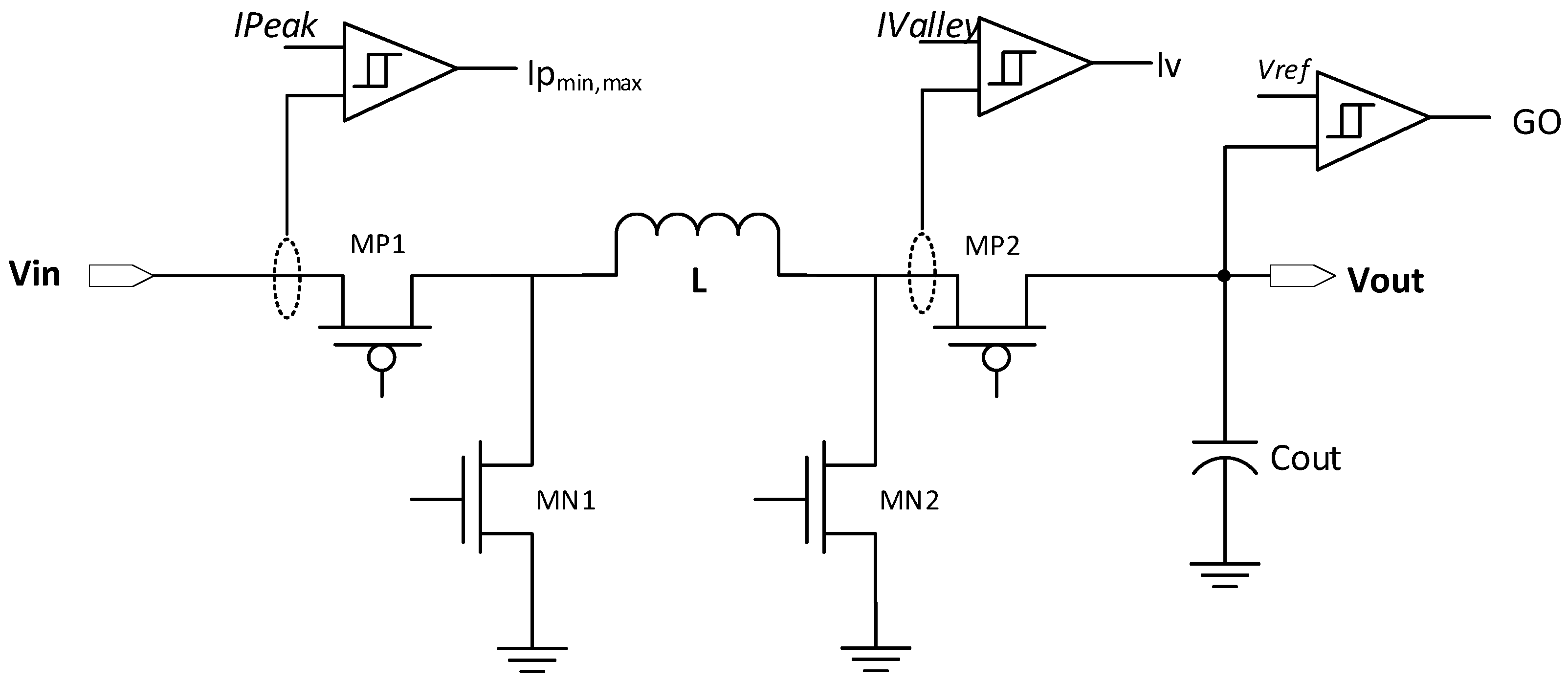
The proposed design methodology was applied to implement an asynchronous controller for a generic buck-boost dc-dc converter whose schematic is depicted in
Figure 1. To avoid subharmonic instabilities, normally IPeak and IValley require more complex slope compensation circuits, which are not considered in this work, as they only change the switching frequency and duty cycle of the converter.
Using a notation like that in [
12],
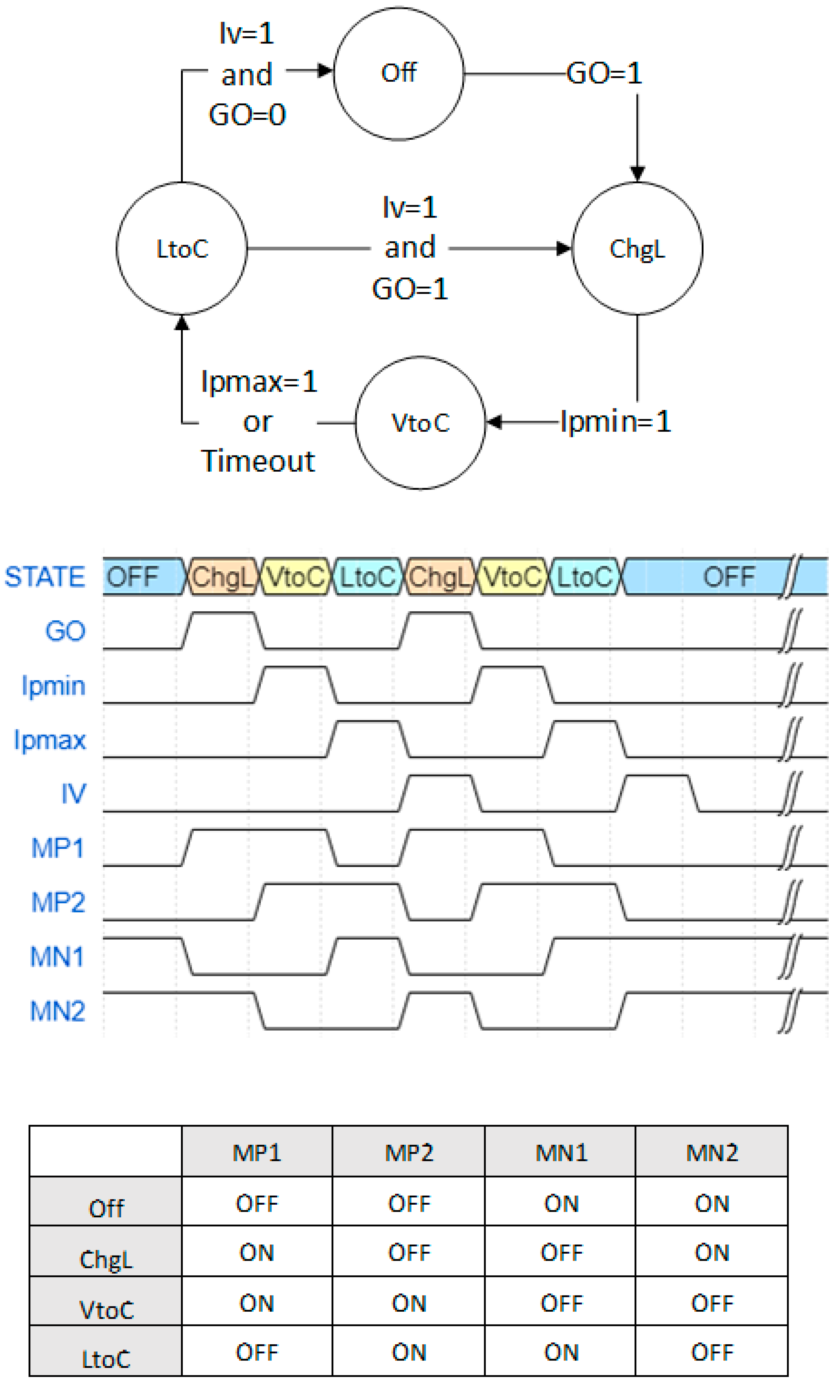
Figure 2 shows the state diagram of the controller (and its ideal timing transitions) where the functions of each state can be summarized as follows:
Off: The initial state and inductor current discharged to Iv (valley level) with Iv > 0 and the off phase lasting for a minimum amount of time (set by intrinsic analog circuits delays) in the continuous mode (CCM) or Iv = 0 and the off phase lasting for a non-minimum amount of time in discontinuous mode (DCM). The off state is exited (and ChgL state is entered) when GO = 1, which occurs sometime after having entered the Off state (DCM) or immediately (CCM).
ChgL: The charge of the inductor until the current reaches the value Ipmin; it is set to zero and the ChgL phase lasts for a minimum amount of time (set by intrinsic analog circuits delays) in the buck condition or set to a positive value and the ChgL phase lasts for a non-minimum amount of time in the boost condition.
VtoC: In the buck mode, there is a further charge of the inductor until the current reaches the value Ipmax set to a positive value, while in the boost mode, the inductor current discharges to the value Iv. In both cases, however, the VtoC phase lasts no more than a certain timeout duration and is then exited.
LtoC: The discharge of the inductor until the current reaches the value Iv. If the current has already reached Iv during the VtoC phase, the LtoC phase has a minimum duration (set by intrinsic analog circuit delays).
3. Proposed Asynchronous Design Methodology
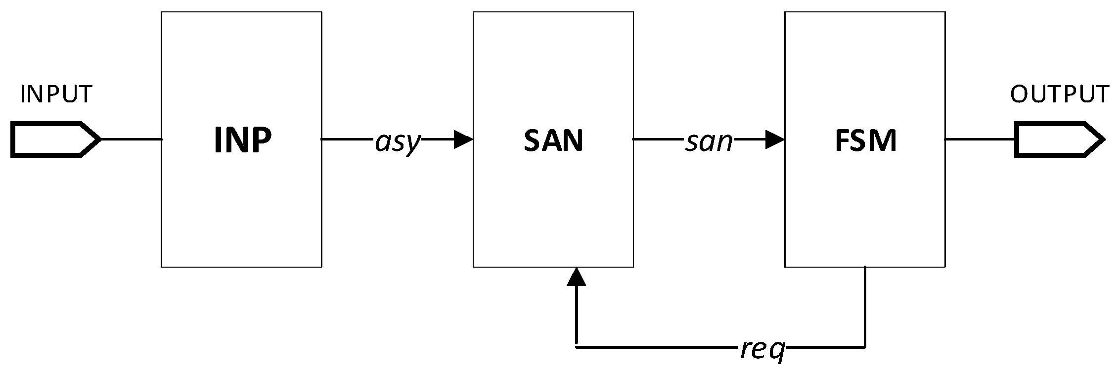
The approach for designing the buck-boost controller is to divide the overall circuit into three sub-blocks, as shown in
Figure 3, where the primary (asynchronous) inputs, the primary outputs, the asy signals which implement the transition conditions of the state diagram of
Figure 2, and the san/req signals which implement the handshake protocol appear. An analysis of each block is provided in the following subsections.
3.1. Finite State Machine Block (FSM)
The FSM block represents the core of the controller, and it implements the true asynchronous machine. As already mentioned, its implementation is based on the use of Workcraft© tool which can synthesize a hazard-free asynchronous circuit if a consistent Signal Transition Graph (STG) is given. An STG is a graphical description of the behavior of an asynchronous circuit based on causal relations between input and output signals. To have a hazard-free circuit, this modeling must guarantee several properties such as deadlock freeness, input properness, and output persistency. All these properties are verified by a suite of tools, including PUNF, MPSAT, PCOMP, and MP2DOT, that provide the verification and synthesis flows based on Petri net and are used by Workcraft© as backends.
The construction of the STG is closely related to the state diagram of
Figure 2, keeping in mind the handshake paradigm on which Workcraft’s automatic synthesis is based [
13]. Basically, in a system without a clock, handshake protocols enable synchronization of asynchronous components through signals (commonly called req and ack) which indicates the completion of a set of instructions.
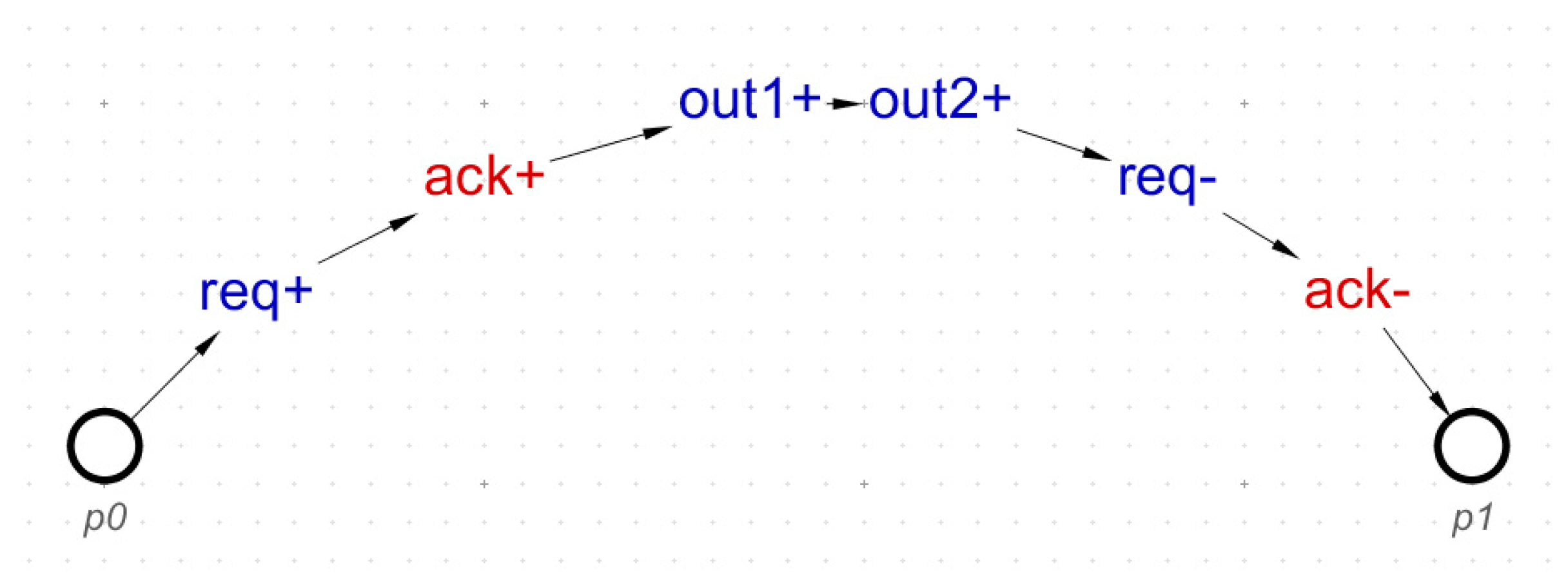
Typically, an STG which models a state transition can be drawn in Workcraft© as depicted in
Figure 4:
For a useful comparison with a synchronous state machine, it is interesting to note that the req signals give an explicit indication of the “current state” and that the output update occurs after the transition between states has been satisfied (i.e., in the “next state”, like Mealy machine).
Figure 5 shows the circuit synthesized by Workcraft© starting from STG that describes the state diagram of
Figure 2 and referring to a proprietary 90 nm technology library. The input signals a, b, c, d, and e represent the transition conditions, as explained later. The circuit also includes the asynchronous reset (rst_n) inserted via the initialization analyzer, which is another built-in utility of the tool, to ensure proper startup of the circuit by providing a known and stable logical value to all nodes in the network.
Observe that the circuit shows several inverters with a dashed line inside. According to the Workcraft’s notation, these inverters have “zero delay” so to honor the “hazard-free” property. Basically, Workcraft’s synthesizer searches for complex gates, in the reference technology library, with complemented inputs (thus considering only one propagation delay in its timing evaluations) and, in the absence of these library cells, it inserts a zero-delay inverter in front of these gates. Satisfaction of this property can, however, be achieved by adding extra efforts during the layout to ensure that the propagation delay of these inverters is much less than the propagation delay of the gate (complex) following them.
3.2. Sanitizer Block (SAN)
The SAN block of
Figure 3 implements the handshake protocol with the finite state machine, ensuring the correct sequence of input to the FSM and thus avoiding the “violation of the environment”, as it is named in Workcraft©.
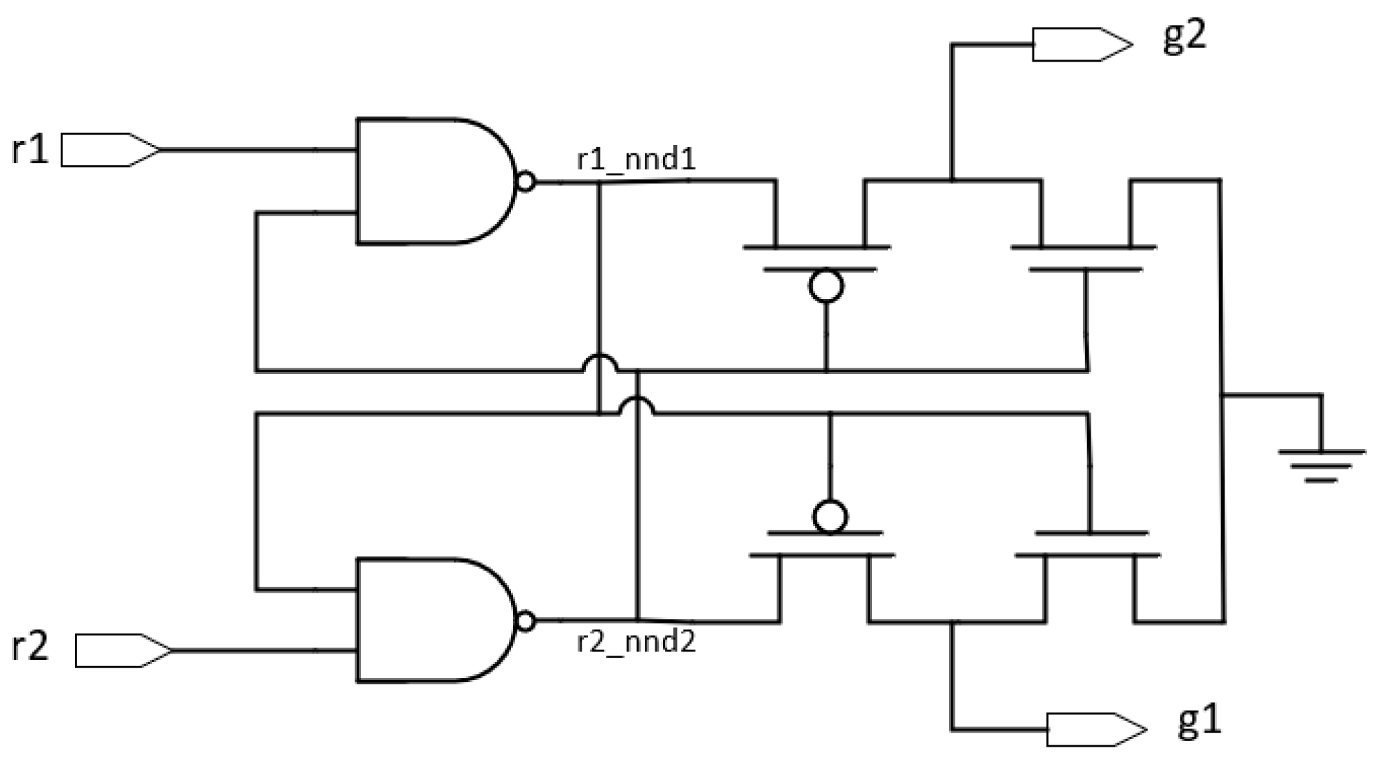
It contains several analog-to-asynchronous (A2A) elements that are arbitration primitives specifically designed to increase the resilience and efficiency in the asynchronous circuits. The fundamental component of these circuits is the mutual exclusion element (MUTEX) [
14,
15], whose circuit is given in
Figure 6.
It consists of a Set–Reset latch followed by an metastability filter that guarantees a fast output signal resolution in case of a simultaneous positive edge from both inputs.
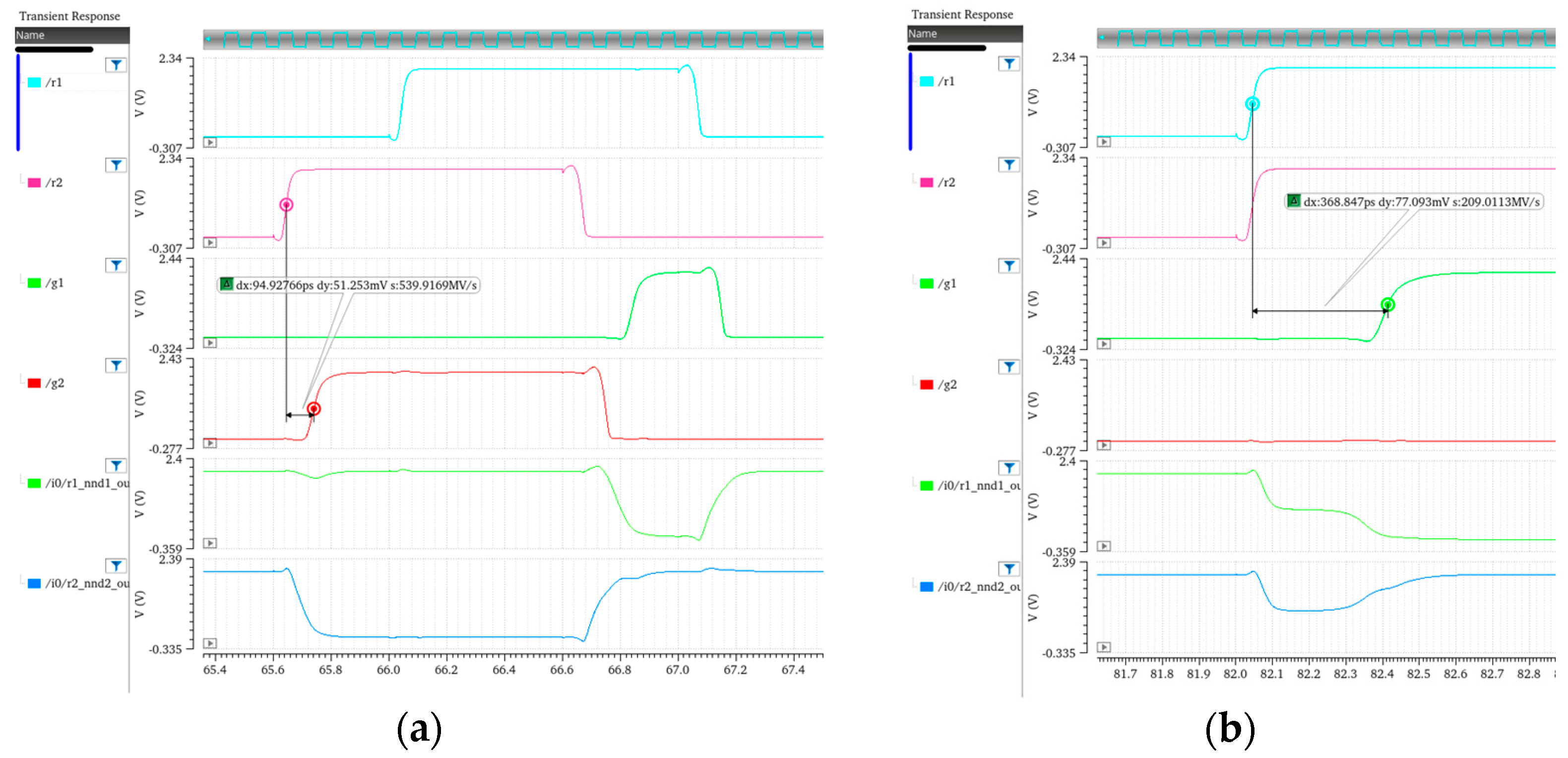
Figure 7 shows the simulation results of the adopted MUTEX considering all possible input transitions. Specifically, non-concurrent input transitions are shown in
Figure 7a, and an input-to-output delay of about 95 ps is measured assuming an input slope of 50 ps.
Figure 7b reports the critical case in which both inputs go high at the same time; from inspection of the figure, it is worth noting that the inner nodes (r1_nnd1 and r2_nnd2) tend to fall and when they reach the logic threshold of the inverters, and these latter resolve (randomly) the outputs’ value in less than 200 ps, leading to an overall input-to-output delay of about 370 ps.
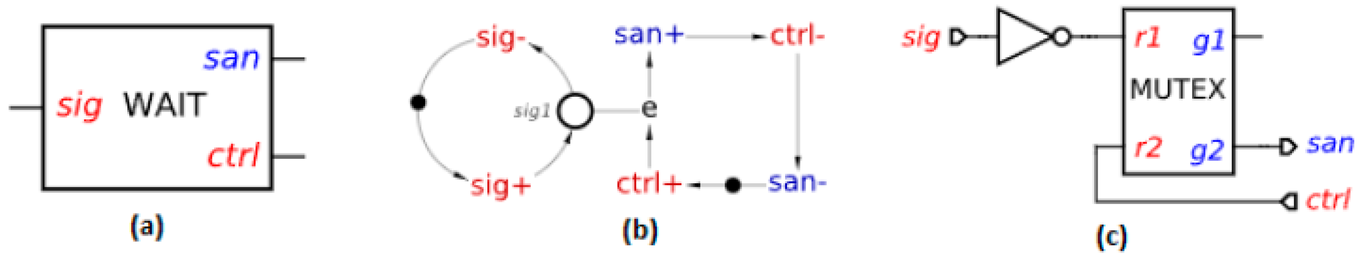
Our controller needs a number of A2A elements equal to the number of inputs of the FSM block. More specifically, we need five WAIT circuits, whose block diagram, Signal Transition Graph, and its implementation are given in
Figure 8.
Basically, it controls an asynchronous handshake ctrl/san for a non-persistent input (sig). According to the STG of
Figure 8b, this element provides a sanitized output (san = 1) if both the ctrl and async input (sig) are high. If ctrl = 0, then san drops to zero and sig is unconstrained and is allowed to switch between 0 and 1 without the output san changing.
Note that we used two WAIT blocks with a common request (req_de) to manage the transitions LtoC- > Off and LtoC- > ChgL because the signals d and e are mutually exclusive and cannot be contemporarily high. For independent inputs, a more complex A2A circuit, called WaitX [
16], must be used. Basically, this circuit, which includes several MUTEX elements and C-elements [
17] (another fundamental cell used in the asynchronous designs), is an element that arbitrates between two non-persistent inputs (sig1, sig2), producing, if enabled by the ctrl signal, only one san output depending on which of the two input signals arrives first.
Others analog-to-asynchronous elements can be used to efficiently design an overall asynchronous circuit; many of these elements are available in [
8].
3.3. Input Block (INP)
The asy signals in
Figure 3 represent the transition conditions in the state diagram and they are implemented into the INP block according to the functions reported in
Figure 2 and rewritten here:
In our case, this block is very simple, including only a few logic gates. Note that any glitches in the asy signals do not reach the FSM circuit because the SAN block decouples the asynchronous machine from the asynchronous and non-persistent input signals.
4. Simulation Results
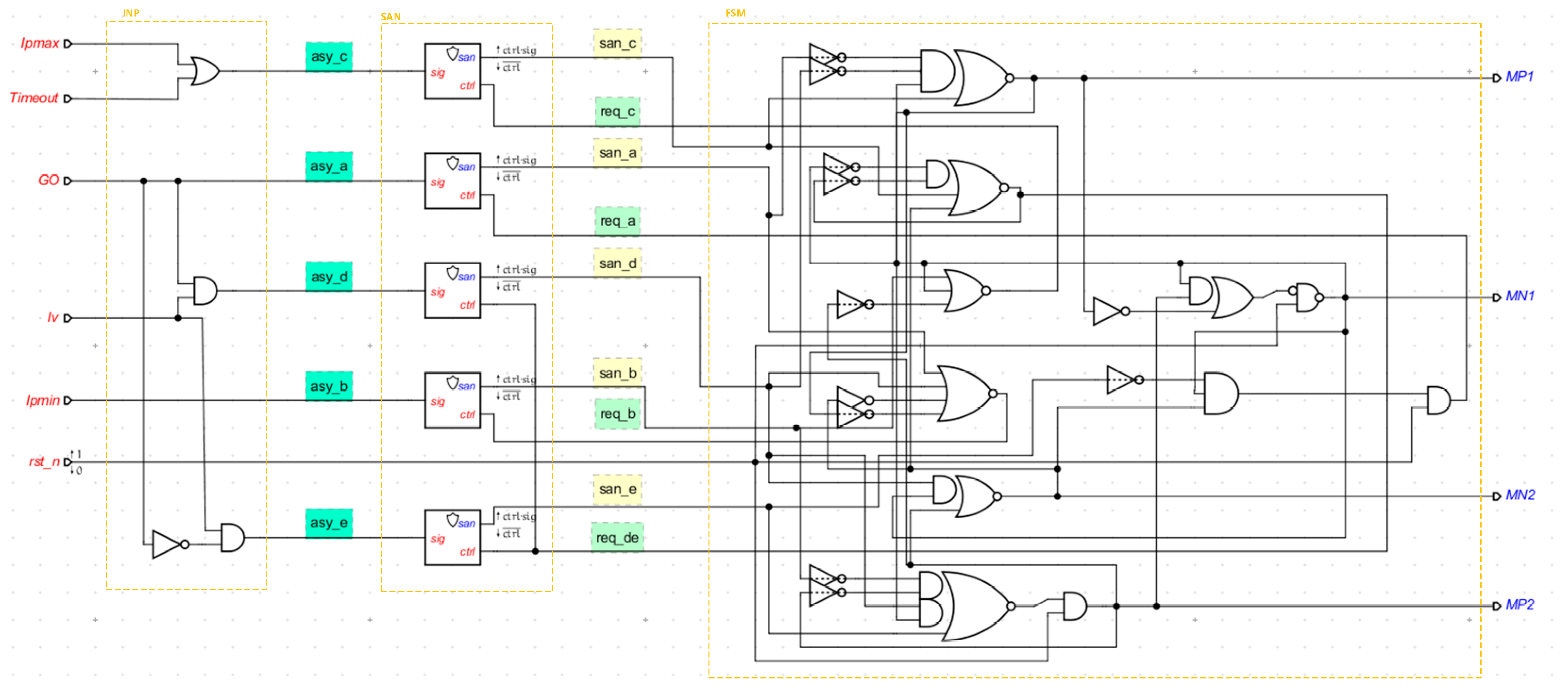
The overall designed controller is shown in
Figure 9, where the blocks described above are highlighted.
The Verilog netlist was extracted from Workcraft and the schematic was created by the Cadence environment in order to run Spectre simulations.
The controller was simulated standalone, stimulating the inputs through a System Verilog (SV) testcase.
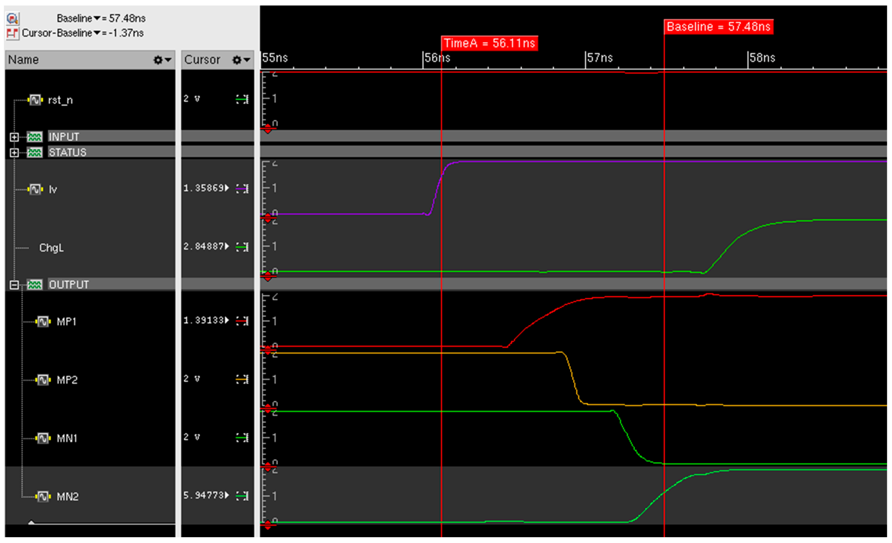
Figure 10 shows the correct evolution of the state diagram of
Figure 2 by changing the input every 10 ns and assuming a realistic rise time of about 700 ps.
Note that the worst input-to-state transition delay (Iv & GO- > ChgL) is about 1.65 ns and occurs when all output signals change, as detailed in
Figure 11.
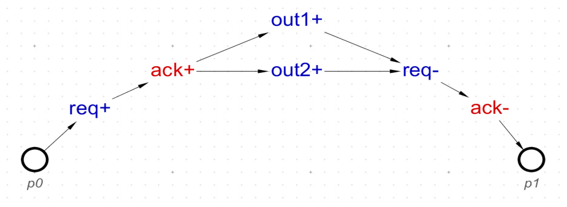
As expected, when Iv goes high, outputs MP1, MP2, MN1 and MN2 toggle in sequence and then the ChgL state signal will be enabled. Obviously, the order in which the output signals are switched must be carefully chosen to avoid any cross-conduction from the power supply to the ground; in this case, it would be better to turn the on switches off first and only then turn the off ones on. However, if the design cannot tolerate any output mismatch, the STG must be redesigned as in
Figure 12, where a parallel connection is adopted.
This design approach ensures simultaneous switching of outputs but increases the number and complexity of the used gates.
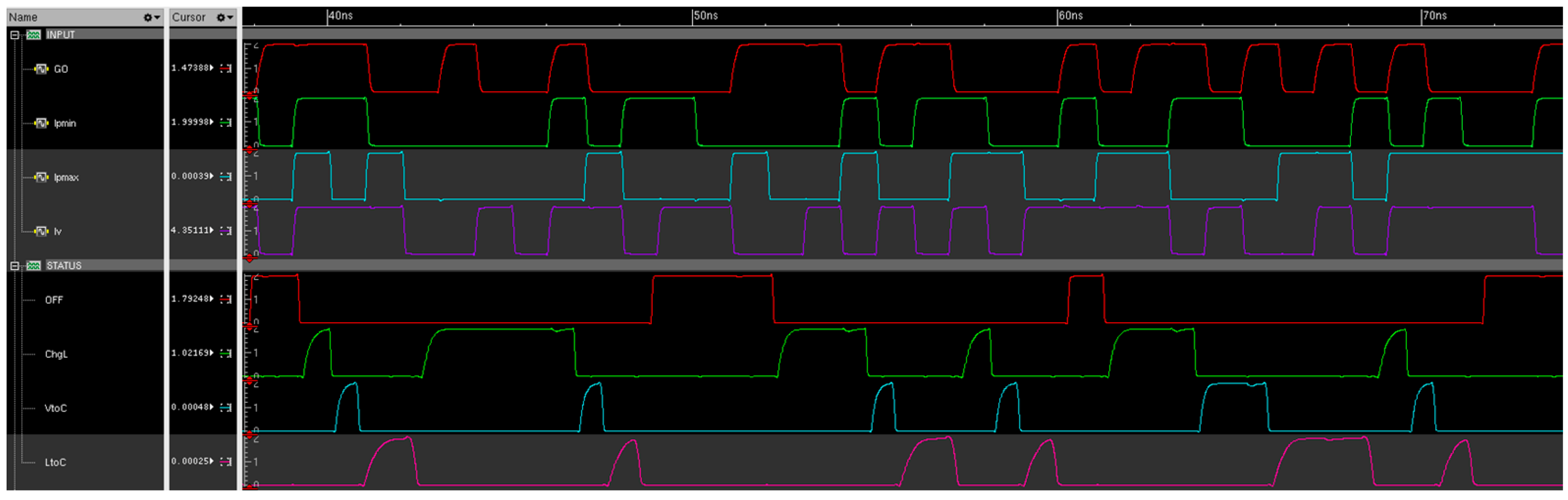
To verify the robustness of the implementation, another SV testcase in which all inputs switch randomly every 1 ns was executed, and the result is shown in
Figure 13. It is easy to see that the controller evolves correctly according to its state diagram, detecting only the enabled asynchronous input and masking all others. The non-overlapping of the state signals also confirms the correct operation.
5. Conclusions
A new and simple procedure for designing high-speed asynchronous controllers useful for DC-DC converters was presented in this paper. The method uses the Workcraft© synthesis tool to implement the asynchronous core of the system and defines the design strategies to implement the other circuits to achieve an efficient and robust asynchronous circuit.
The design example was designed to control a generic buck-boost converter, and simulation results (using a proprietary 90-nm technology) demonstrated the validity of the proposed approach, showing a time response between input and output of less than 1.4 ns and proper functionality for random, non-persistent asynchronous input signals. Note that an equivalent speed result can be achieved by implementing a synchronous controller clocked @700 MHz with a huge dynamic power consumption.
The literature reports many comparisons of energy efficiency between asynchronous and synchronous circuits [
18,
19] demonstrating energy savings of more than 50%, although this percentage is highly dependent on the specific design and application.
Two asynchronous controllers, designed following the discussed methodology, were successfully implemented in the PMIC MAX20362 to realize a very fast controller and arbiter for an SIMO (single input multiple output) buck-boost converter.
The proposed approach seems to also be able to include a scan test circuit with a modest increase in resources and by designing elementary mutex and c-elements with scanning capabilities. This aspect is currently under investigation.
Author Contributions
Writing—original draft preparation, R.M. and A.M.; writing—review and editing, R.M. and A.M. All authors have read and agreed to the published version of the manuscript.
Funding
This research received no external funding.
Institutional Review Board Statement
Not applicable.
Informed Consent Statement
Not applicable.
Data Availability Statement
The original contributions presented in this study are included in the article. Further inquiries can be directed to the corresponding author(s).
Conflicts of Interest
The authors are from Company Analog Devices. The authors declare no conflicts of interest.
References
- Furber, S.B.; Garside, J.D.; Riocreux, P.; Temple, S.; Day, P.; Liu, J.; Paver, N.C. AMULET2e: An asynchronous embedded controller. Proc. IEEE 1999, 87, 243–256. [Google Scholar] [CrossRef]
- Kessels, J.; Marston, P. Designing asynchronous standby circuits for a low-power pager. Proc. IEEE 1999, 87, 257–267. [Google Scholar] [CrossRef]
- Nielsen, L.S.; Sparso, J. Designing asynchronous circuits for low power: An IFIR filter bank for a digital hearing aid. Proc. IEEE 1999, 87, 268–281. [Google Scholar] [CrossRef]
- Zhu, J.; Ding, G.; Song, B.; Zhang, F. An Adaptive Delay Error Asynchronous Circuit Design Based on Bundled-Data Handshake Protocol. In Proceedings of the 7th International Forum on Electrical Engineering and Automation (IFEEA), Hefei, China, 25–27 September 2020. [Google Scholar]
- Peeters, A.; de Wit, M. Asynchronous circuit design using Handshake Solutions. In Proceedings of the IEEE International SOC Conference, Newport Beach, CA, USA, 17–20 September 2008. [Google Scholar]
- Oliveira, D.L.; Bompean, D.; Faria, L.; Curtinhas, T.; Alles, N. Design of Asynchronous Digital Systems using Two-Phase Bundled-Data Protocol. In Proceedings of the VI Andean Region International Conference, Cuenca, Ecuador, 7–9 November 2012. [Google Scholar]
- Yun, K.Y.; Beerel, P.A.; Arceo, J. High-performance two-phase micropipeline building blocks: Double edge-triggered latches and burst-mode select and toggle circuits. IEE Proc. Circ. Dev. Sys. 1996, 143, 282–288. [Google Scholar] [CrossRef]
- Workcraft. Available online: https://workcraft.org (accessed on 1 January 2024).
- Sokolov, D.; Khomenko, V.; Yakovlev, A.; Lloyd, D. Design and Verification of Speed-Independent Circuits with Arbitration in WORKCRAFT. In Proceedings of the 24th IEEE International Symposium on Asynchronous Circuits and Systems, Vienna, Austria, 13–16 May 2018; pp. 30–31. [Google Scholar]
- Petrify. Available online: https://www.cs.upc.edu/~jordicf/petrify (accessed on 1 January 1999).
- Kushnerov, A.; Bystrov, S. Signal Transition Graphs for Asynchronous Data Path Circuits. Mod. Anal. Inf. Sys. 2023, 30, 170–186. [Google Scholar] [CrossRef]
- Fernandez, D.; Madrenas, J.; Alarcon, E. An asynchronous finite state machine controller for integrated buck-boost power converters in wideband signal-tracking applications. In Proceedings of the 2008 IEEE International Symposium on Circuits and Systems (ISCAS), Seattle, WA, USA, 18–21 May 2008; pp. 2210–2213. [Google Scholar]
- Peeters, A.M.G. Single-Rail Handshake Circuits. Ph.D. Thesis, Eindhoven University of Technology, Eindhoven, The Netherlands, 1996. [Google Scholar]
- Swathi, R.; Srinivas, M.B. All Digital Duty Cycle Correction Circuit in 90nm based on mutex. In Proceedings of the IEEE Computer Society Annual Symposium on VLSI, Tampa, FL, USA, 13–15 May 2009; pp. 258–262. [Google Scholar]
- Zhang, Y.; Heck, L.S.; Moreira, M.T.; Zar, D.; Breuer, M.A.; Calazans, N.L.; Beerel, P.A. Testable MUTEX Design. IEEE Trans. Circ. Syst. I 2016, 63, 1188–1199. [Google Scholar] [CrossRef]
- Khomenko, V.; Sokolov, D.; Mokhov, A.; Yakovlev, A. WAITX: An Arbiter for Non-persistent Signals. In Proceedings of the 2017 23rd IEEE International Symposium on Asynchronous Circuits and Systems (ASYNC), San Diego, CA, USA, 21–24 May 2017; pp. 33–40. [Google Scholar]
- Emmert, J.M.; VanDewerker, S.A. EMC: Efficient Muller C-Element Implementation for High Bit-width Asynchronous Applications. In Proceedings of the 2021 IEEE International Midwest Symposium on Circuits and Systems (MWSCAS), Lansing, MI, USA, 9–11 August 2021; pp. 816–819. [Google Scholar]
- Akgun, O.C.; Leblebici, Y. Energy Efficiency Comparison of Asynchronous and Synchronous Circuits Operating in the Sub-Threshold Regime. J. Low Power Electron. 2008, 4, 320–336. [Google Scholar] [CrossRef]
- Pandey, B.; Yadav, J.; Singh, Y.K.; Swarnkar, P. Energy efficiency of asynchronous and synchronous VLSI circuit on 40nm and 90 nm FPGA. In Proceedings of the International Conference on Energy Efficient Technologies for Sustainability, Nagercoil, India, 10–12 April 2013. [Google Scholar]
| Disclaimer/Publisher’s Note: The statements, opinions and data contained in all publications are solely those of the individual author(s) and contributor(s) and not of MDPI and/or the editor(s). MDPI and/or the editor(s) disclaim responsibility for any injury to people or property resulting from any ideas, methods, instructions or products referred to in the content. |
© 2024 by the authors. Licensee MDPI, Basel, Switzerland. This article is an open access article distributed under the terms and conditions of the Creative Commons Attribution (CC BY) license (https://creativecommons.org/licenses/by/4.0/).
