1. Introduction
Among the design flow steps, the verification phase has become increasingly important and has grown in complexity: this is especially true for non-volatile memories (NVMs) such as NOR Flash or equivalent technology.
The NVM macrocells being verified by the presented flow range from 128 KB up to >4 MB memory, and operate within a wide voltage range (e.g., 1.2 V supply and up to ~15 V internal nets). On the analog side, they may have one or more memory cell arrays with a complex periphery (row/column decoding), read/write management, test management, several charge pumps, digital-to-analog converters (DACs), internal current/voltage references, oscillators, and so forth. The digital blocks include finite state machines, microcontrollers, registers, read-only memories (ROMs), and random-access memories (RAMs). The interaction of all parts must be verified with extreme confidence before proceeding to industrialization [
1].
Such designs, in fact, require a comprehensive list of verifications with up to 200 full-chip simulation patterns (excluding pure digital simulations, which may sum to many tens of thousands). Analog simulation tools, though highly accurate, are insufficient to achieve fast performance, early debugging, and wide coverage in such a complex environment: that is why co-simulations (also analog mixed-mode simulations, AMSs) must be used, based on the interaction of digital and analog simulation tools [
2].
However, a number of full transistor-level simulations (i.e., completely analog verifications) are still mandatory to extract crucial data such as accurate timings and power consumption. Normally, the approach to these simulations is different from the pure AMS approach because they require a different environment (netlist, input stimuli, etc.). The presented methodology unifies the various simulation types (from fully digital to full transistor) in a comprehensive and flexible environment.
4. The Complete Co-Simulation Environment
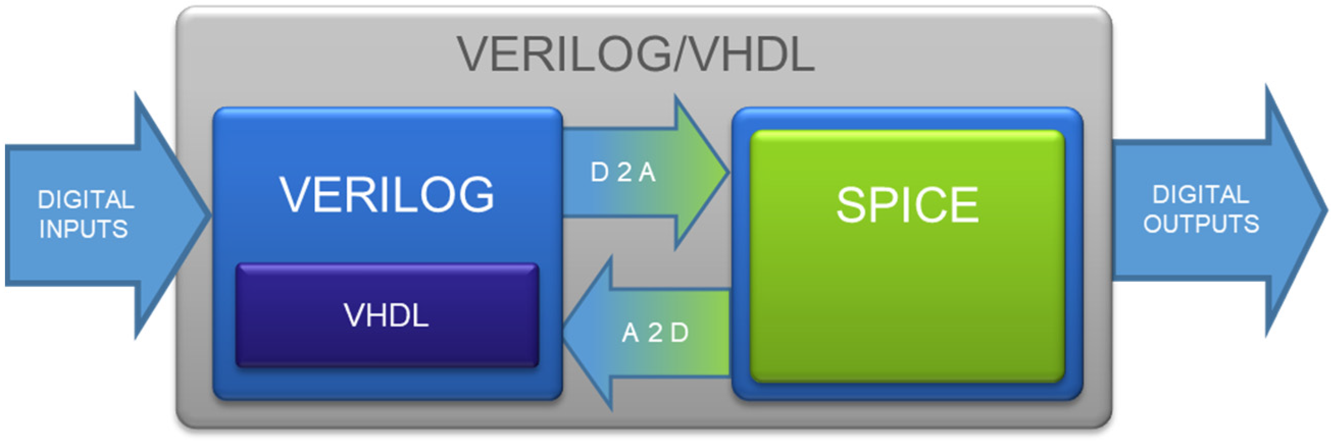
Having presented the basic architecture of the co-simulation scheme, it is time to explore the various environment options, based on verification purposes (mainly, accuracy and performance). The starting point is again the scheme of
Figure 11, redrawn as shown below in
Figure 16.
This general-purpose scheme is applicable for any AMS verification environment with a transistor-level part (SPICE) managed by the analog simulator and a digital part (RTL) managed by the digital simulator. Input stimuli are provided in digital format (such as .tcl commands), and both analog and digital outputs are normally available. This is a sort of ideal combination in which the analog circuitry is solved with very high accuracy and the digital one is managed with the highest speed; starting from this, it is possible to build the two other combinations for the extreme cases of fully digital and fully analog verifications.
4.1. Fully Digital Environment
To perform a huge set of functional verifications which cover many combinations of input sequences and/or digital states (e.g., registers contents), the best choice is a fully digital environment where the analog blocks are either modeled by some RTL language (like System Verilog) or described at high level by a more or less detailed behavioral model [
5]. The easy replacement of the whole analog part may lead to the situation shown in
Figure 17 (where BEH stands for the digital behavioral model block).
This solution provides the widest coverage: the analog details are lost (e.g., internal voltages/currents, power consumption, transition timings) but, thanks to the computational speed of pure digital simulations, the amount of stimuli/states combinations is in the range of thousands. This is extremely important for the careful verification of RTL codes, ROM algorithms, settings, and timings in all combinations, even randomized combinations.
As mentioned in
Section 3.4.3, after the RTL code is complete, the logic is synthesized at gate level and the process of Place&Route is performed to optimize area occupation, propagation delays, and gate density; then, the RTL can be replaced with an extracted Verilog netlist (which is also back-annotated with the capacitive loads) for better simulation confidence.
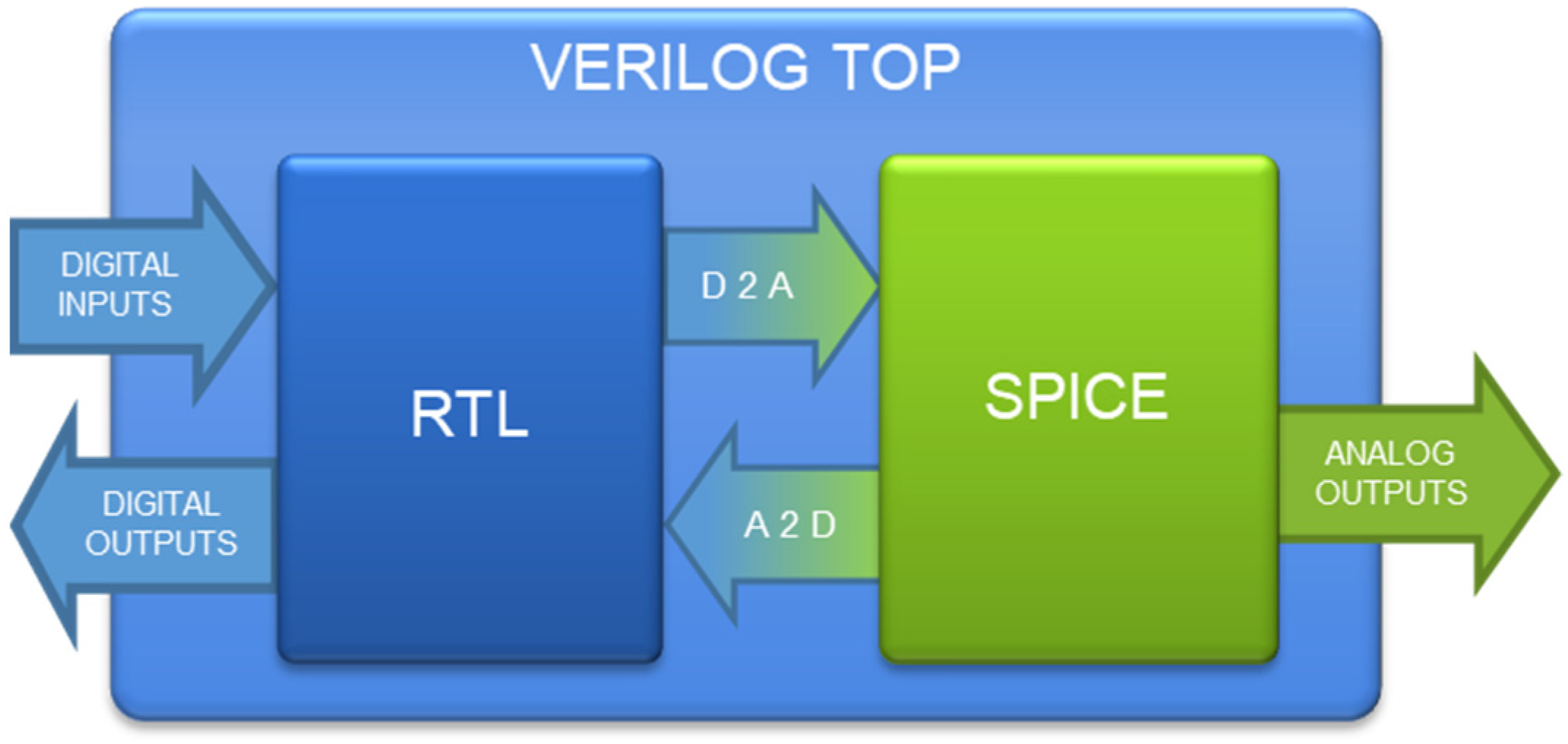
4.2. Fully Analog Environment
On the other hand, the highest accuracy can only be achieved using a fully analog environment (wherein everything is placed at the transistor-level, including digital blocks, with no modeling at all); that is the only way to extract a complete picture of voltages, currents, timings, and power in any combination of process corners, voltage supply, and temperature (PVT) [
6]. This implies that such simulations are highly detailed but very slow.
In general, the fully analog environment is quite modified compared to the ones shown so far, which are based on a Verilog top and contain a selection of RTL, behavioral or SPICE blocks inside. The scheme is illustrated in
Figure 18.
Here, there is at least one big difference: the input stimuli cannot be described as digital sequences, but in a SPICE-like transient format (such as .pwl). As an example, to set a signal Input1 from low to high level at t = 100 ns and back to low after 200 ns, in .tcl format, the command sequence is similar to the following:
Meanwhile, in SPICE format, with Gnd = low (0 V) and Vdd = high, the sequence is more similar to the following:
which is less readable and hardly editable.
In addition to this, the simulation environment must be rewritten and the whole flow is different: the poor reuse of existing files is possible, with a loss of time and resources and a risk of misalignment against the other environments.
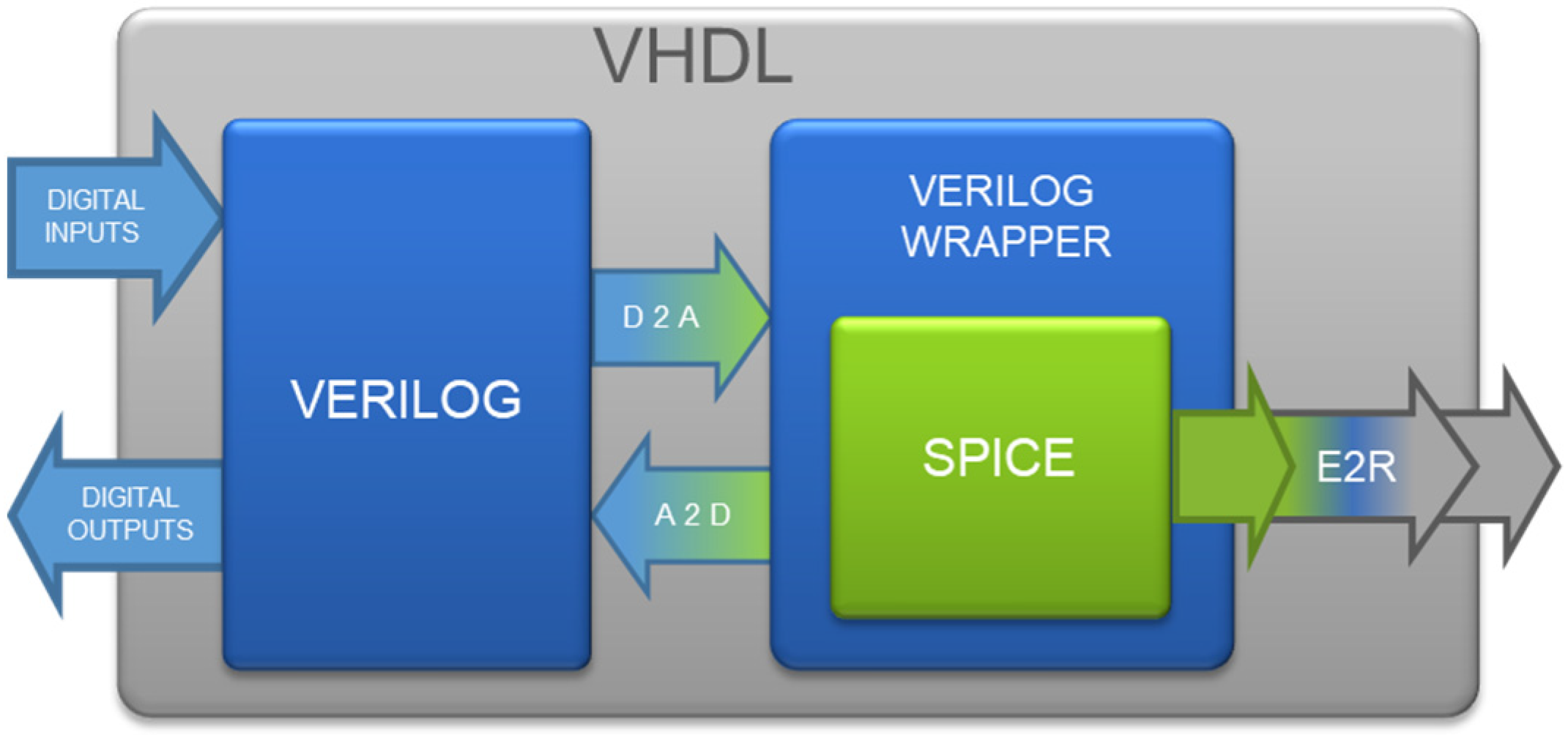
4.3. Fully Analog Environment with Verilog Top
There is a simple and effective solution to the problems mentioned above. As stated in 3.4.2, encapsulating SPICE blocks inside a Verilog top does not at all alter the connectivity and propagation of analog nets; then, it is possible to place the analog blocks of
Figure 18 in the same Verilog top used in the existing AMS environment (
Figure 16).
In order to allow the full reuse of input stimuli in digital format, the only small update which is required is the generation of D/A (input) and A/D (output) converters in the Verilog top itself; this way, the SPICE blocks have full connectivity to the external digital boundary.
As shown in
Figure 19, the final scheme shares the digital-on-top approach with the AMS scheme, allowing for the complete compatibility of simulation features. The transition from one environment to the other is easy, straightforward, and more reliable.
4.4. Interchangeability of the Environments
The tools allow for the easy replacement of alternative “views” for subcircuits (analog or digital model); using the configuration file vcsAD.init, it is possible to choose according to the specific needs of each simulation, as follows:
use_spice -cell top_analog for transistor-level topview
use_verilog -module chargepump.sv for System Verilog model
use_verilog -module oscillator.sv for System Verilog model
Therefore, tuning the trade-off between accuracy and performance is just a matter of simulation purpose. Usually, the verification environments are kept separated and run in sequence: first, the large number of mixed-mode simulations, then the smaller quantity of fully analog ones. Fully digital simulations are not normally run by analog designers and are made available just for quick checks or verification of the behavioral model coherence.
4.5. Selection Criteria
The choice is based on experience as well as coverage requirements; as an example, an operation of programming a word in the NVM array can be performed in a large variety of parameter combinations, such as address (row/column) of the word, previous content, programming efficiency, voltage levels, and pulse duration.
Therefore, what normally happens is that, starting from a verification plan which may include several hundreds (or more) of different digital simulation patterns, a subset is selected to run the mixed-mode simulations (usually in the range of 150–200 for NVMs), and then, a shorter list (from 20 to 40) is chosen for fully analog simulations.
In a fully digital environment, it is feasible to test most combinations (including the ones which are properly modeled for analog behaviors), checking the effect of the parameters on the simulation’s outcome.
In a mixed-mode environment instead, a limited number of sample cases is used (e.g., min. and max. voltage level, extreme PVT corners, with cells that require more attempts to be programmed, and so on); this is obviously due to the duration of each simulation, which may range from hours to 1 or 2 days. Other kinds of more complex simulations, like the erasing of a page, will often need up to 3–4 weeks to be completed.
Finally, in a fully analog testbench, the list of simulations is shortened to the typical functionality cases and some worst cases, such as highest consumption or slowest reading access. The duration of a full-transistor simulation is up to >2X the equivalent AMS one.
5. Stimuli and Testbenches Generation Methods
AMS simulations are mainly used to find issues that are not detectable when using digital simulations: mostly, such issues can be related to analog circuits that are not properly modeled in fully digital simulations. Digital simulations, on the other hand, are thousands of times faster than AMS simulations; therefore, they can perform huge numbers of basic operations, playing with randomness in operation sequences, addresses, and data, exploring all possible features in the device under test (DUT) and aiming to achieve the best verification coverage.
It is impractical to run the same testbenches used in digital simulations for AMS simulations; therefore, AMS testbenches are generally quite different from the ones used for digital simulations. However, some common libraries can be shared for the basic procedures, when developing testbenches for digital and AMS simulations; indeed, the signal sequences sent to the devices, as well as the signal setup and hold with respect to the clocks, are the same in both the analog and digital environments.
This gives the advantage that the basic operations are performed using the same elementary bricks. Moreover, if the same procedures are shared between the two environments, the update and maintenance are faster and safer.
Our testbenches for AMS are built using those common libraries: in some cases, the mixed-signal testbench can simply be a lighter version of the digital one (e.g., by reducing the loop number parameter from thousands to one or two).
Two main scenarios have been explored and implemented: one is based on the interactive shell of VCS digital simulator, ucli (which is a tcl shell), and the other one is based on a fully Verilog/System Verilog-based environment.
5.1. Interactive Approach
This approach has been widely used for several years, and it is basically applied to the environment shown in
Figure 16.
Testbenches are a collection of tcl files, which are, in general, labeled depending on the device function they are used to test, are sourced at VCS tcl-ucli interface, and reuse the basic libraries that implement the basic operations developed with the same tcl language.
The basic operations inside the libraries are, in general, parametric tcl procedures, such as the following:
proc prog_data { address data } {...}.
The tcl testbench can force digital inputs, read digital outputs, read analog inputs, and sample the internal signals in the design on both the analog and the digital side using the proper commands.
The capability of reading back the outputs and sniffing the internal signals provides the possibility of implementing automatic checks on both the analog and the digital side; since, in AMS simulation, the more time-consuming engine is the analog one, the overhead of such checks is negligible with respect to the overall simulation time, while being extremely efficient compared to direct visual checks by the user.
Another advantage of this approach is the capability of interactive debugging of the testbench itself, using the VCS tcl-ucli interface.
Using this approach, there is a great benefit in the speed of the AMS scheme, because the start-up phase (also known as power-on-reset, POR) can be executed only once and reused for the next simulations. When the analog voltages are ramping up at POR, the simulation can be very slow; moreover, during this phase, the memory trimmings and configurations are loaded as well, so skipping it in subsequent simulations greatly reduces the simulation time.
Sometimes, it is possible to face issues when specific tcl commands are customized for one digital simulator and not supported by another one. In this case, it is necessary to replace those commands by hand-adapting the syntax, which is a nuisance.
5.2. Batch Approach
The complexity of NVM memory designs is continuously growing: an alternative methodology to the interactive approach is provided by testbenches written in Verilog/System Verilog languages. System Verilog also offers a more accurate style for modeling, and stimuli sequences are more readable and reusable. In addition, associative arrays, assertions/checkers, and concurrency provide an added value in terms of quality and compatibility [
6].
It is not the scope of this article to go into detail about Verilog and System/Verilog capabilities: it is enough to mention that the approach has been used for digital full-chip and AMS environments in 18 nm technology.
An additional Verilog testbench level must be added, which encloses the TOP_VERILOG that becomes the DUT, as shown in
Figure 20. This time, AMS verifications are run in the
Synopsys XA-VCS environment, while fully digital verifications make use of the
Cadence simulation tool.
Although the two environments are different, the testbench structures are shared between fully digital top simulations and AMS simulations: only the core code of the testbench needs to be modified by limiting the number of the DUT input sequences, in order to have a reasonable duration of AMS simulations.
Also, in this approach, a collection of elementary procedures/commands has been developed to perform the basic operations; as an example, a Verilog task could be as follows:
function [31:0] get_configuration;
input [17:0] conf_add;
begin
{…}
get_configuration = read_data;
end
endfunction
All the tasks are, in general, placed in a specific file or package which is included or declared using the include or import directives.
Thanks to the concurrency, it is easy to parallelize and build more complex stimuli with an enhanced ease of use.
The same System Verilog assertions used for digital full-chip simulations can be reused in the AMS digital side, improving the quality of simulations without affecting the simulation runtime. In addition, other assertions can be built for the analog side of AMS using the real numbers features that have been introduced in System Verilog.
When writing assertions or checks on signals, it is recommended to use (when possible) not internal block signals but internal pins, to be sure that the name is also preserved in the gate-level netlist; this allows for the reusability of the assertion/check approach for back-annotated AMS simulations which use SDF files.
One major difference with respect to the interactive approach is that Verilog/System Verilog testbenches are run in batch mode (compiled first, then executed) so the user loses interactivity with the simulator, which is very useful in the early debug phase.
6. Conclusions
As can be seen from the common Verilog top presented in
Section 4, from an external point of view, all the verification environments look the same: they have the same pinout and internal structures, which, whether digital or analog, generate the same outputs after the same input sequences.
In other words, there is a smooth and seamless transition from fully digital simulations (RTL logic + BEH analog), through mixed-mode ones (RTL logic + SPICE analog), to fully analog verifications (wherein everything is transistor-level).
This allows for the efficient and flexible reuse of input stimuli and other required files (e.g., array contents, configurations, and output checks).
By keeping most environment features in common, verification designers can easily exchange data, stimuli, and results, thus enhancing debug capabilities and reducing simulation time. The comparison between behavioral models and their analog counterparts is also easily achieved for the easier debug and maintenance of the models themselves.
The presented approach has been adopted for the last decade on tens of projects in different technology nodes with very good results and is currently under continuous evolution and enhancement.


