
Silicon Radiation Detector Technologies: From Planar to 3D


Abstract
1. Introduction
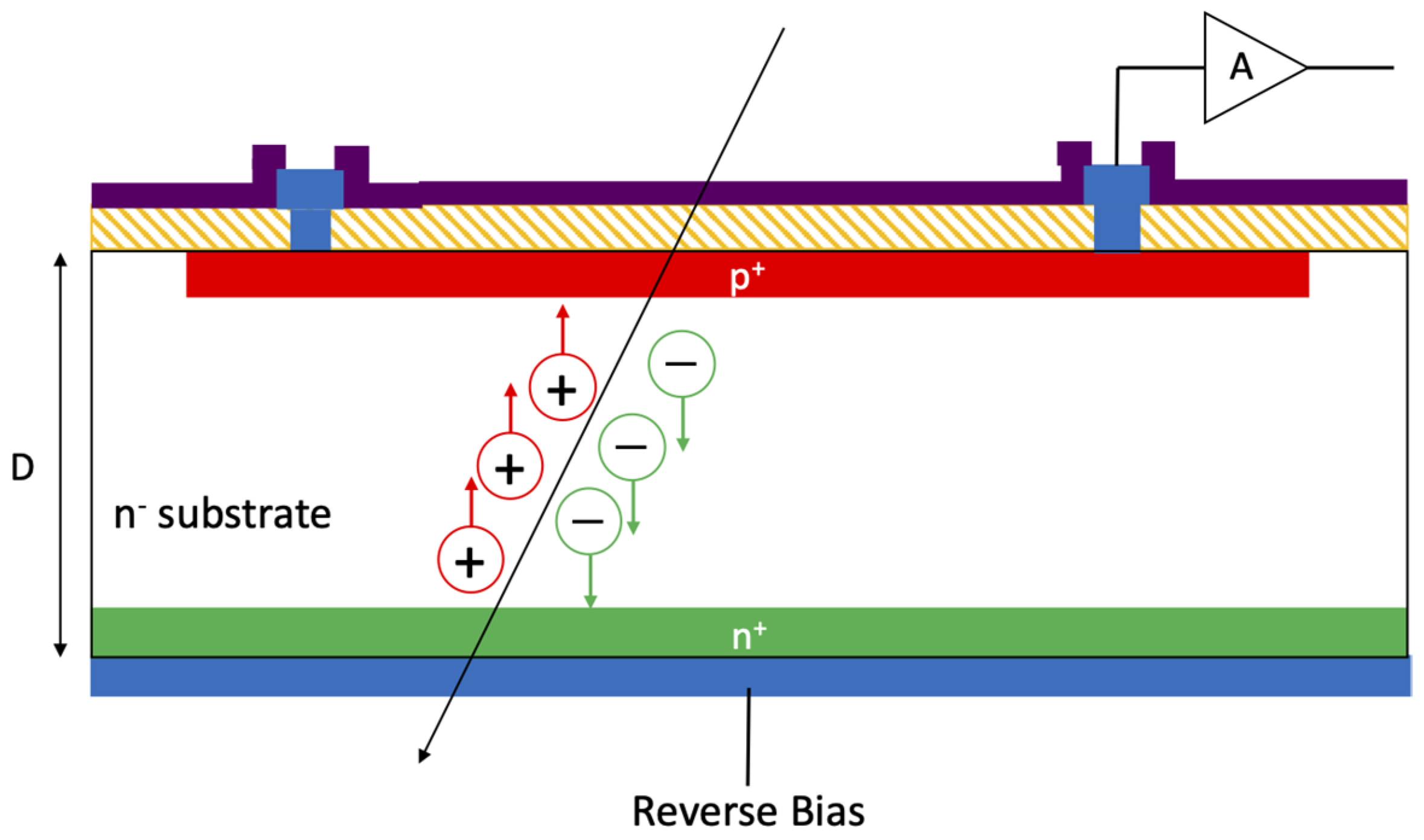
2. Basic Principles and Requirements
- Very low leakage currents. Besides affecting power dissipation, the leakage current plays a critical role in the detector noise, so it should be minimized. A value < 1 nA/cm2 is normally assumed as a target. The leakage current is mainly caused by thermal generation in the depleted bulk, so the carrier lifetimes should be high enough, calling for high-purity material and ultra-clean processing, as well as for an optimized layout, often including guard rings [5].
- Large breakdown voltage. In certain cases, detectors require extremely high voltage to operate effectively. This may be due to factors such as thick substrates, the necessity to achieve high electric fields for velocity saturation, or radiation damage. Specifications often require the breakdown voltage to exceed several hundreds of volts. The use of guard rings is also useful in this respect [6].
- Radiation hardness. This is especially the case of detectors used in HEP experiments at particle colliders, where the fluences can be as large as ~1016 1-MeV equivalent neutrons per square cm (neq/cm2). Displacement damage to the silicon lattice is here the main issue, with three main consequences [7]: (i) increase in leakage current (linear with fluence); (ii) change in the effective space-charge concentration, leading to an increase in depletion voltage at large fluences; (iii) charge carrier trapping, which represents the factor ultimately limiting the detector performance at fluences beyond~1015 neq/cm2. In addition, ionization damage effects [8] are caused by charged particles but also by high-energy photons (X- and γ-rays), with total ionizing doses that can largely exceed 1 Grad in applications at particle colliders and at Free Electron Laser facilities [9]. The consequences are the build-up of positive charge in the oxides and of interface states, which affect the isolation between n+ regions, the parasitic capacitance between adjacent regions (with impact on noise), the electric fields at the surface (with impact on breakdown voltage) and surface generation/recombination (with impact on leakage current and charge collection in case radiation is absorbed near the surface).
- In silicon detectors, the minimum feature sizes are not too small (~micrometers). Proximity lithography is mainly used, sometimes with double-side alignment. The overall device dimensions can be very large (up to tens of square centimeters) and the specifications often require the total number of defects to be very small, so that yield is certainly a major concern in detector fabrication.
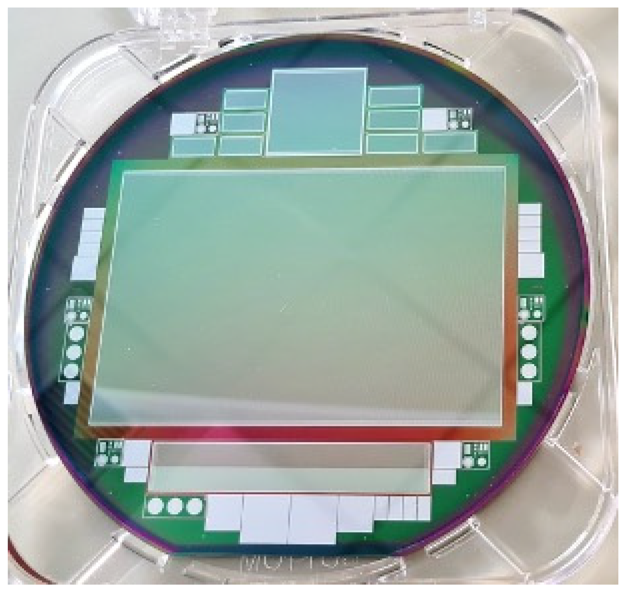
3. Fabrication Technologies
3.1. Starting Material
- Neutron-transmutation-doped (NTD) substrates [11] are obtained from the irradiation of high-purity p-type silicon with fast neutrons, yielding n-type material with high-resistivity up to 5 kΩ cm. NTD wafers feature the lowest non-uniformities in the doping concentration, down to 5%, which is important for some types of detectors (e.g., drift detectors).
- Czochralski (CZ), Magnetic Czochralski (MCZ) and epitaxial wafers have also been recently used for the fabrication of silicon detectors in HEP applications. In fact, these types of substrates have a high concentration of oxygen, in the range of 1017–1018 cm−3, which was found to be beneficial in terms of radiation hardness of the detectors, since it lowers the increase in the effective space charge concentration at high radiation fluences, thus reducing the depletion voltage [12].
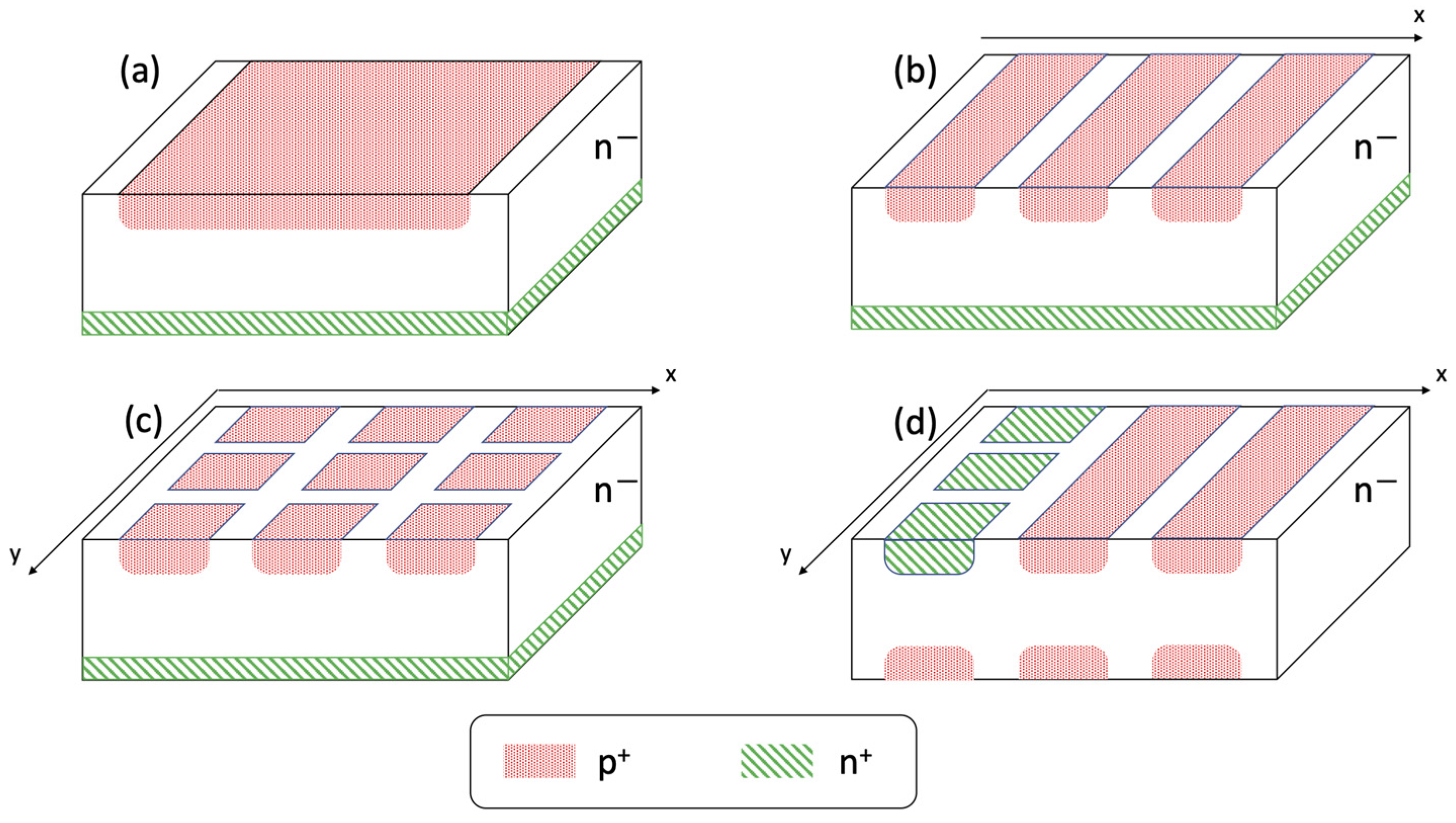
3.2. Planar Technology
3.2.1. Common Detector Types
3.2.2. Technological Aspects
- -
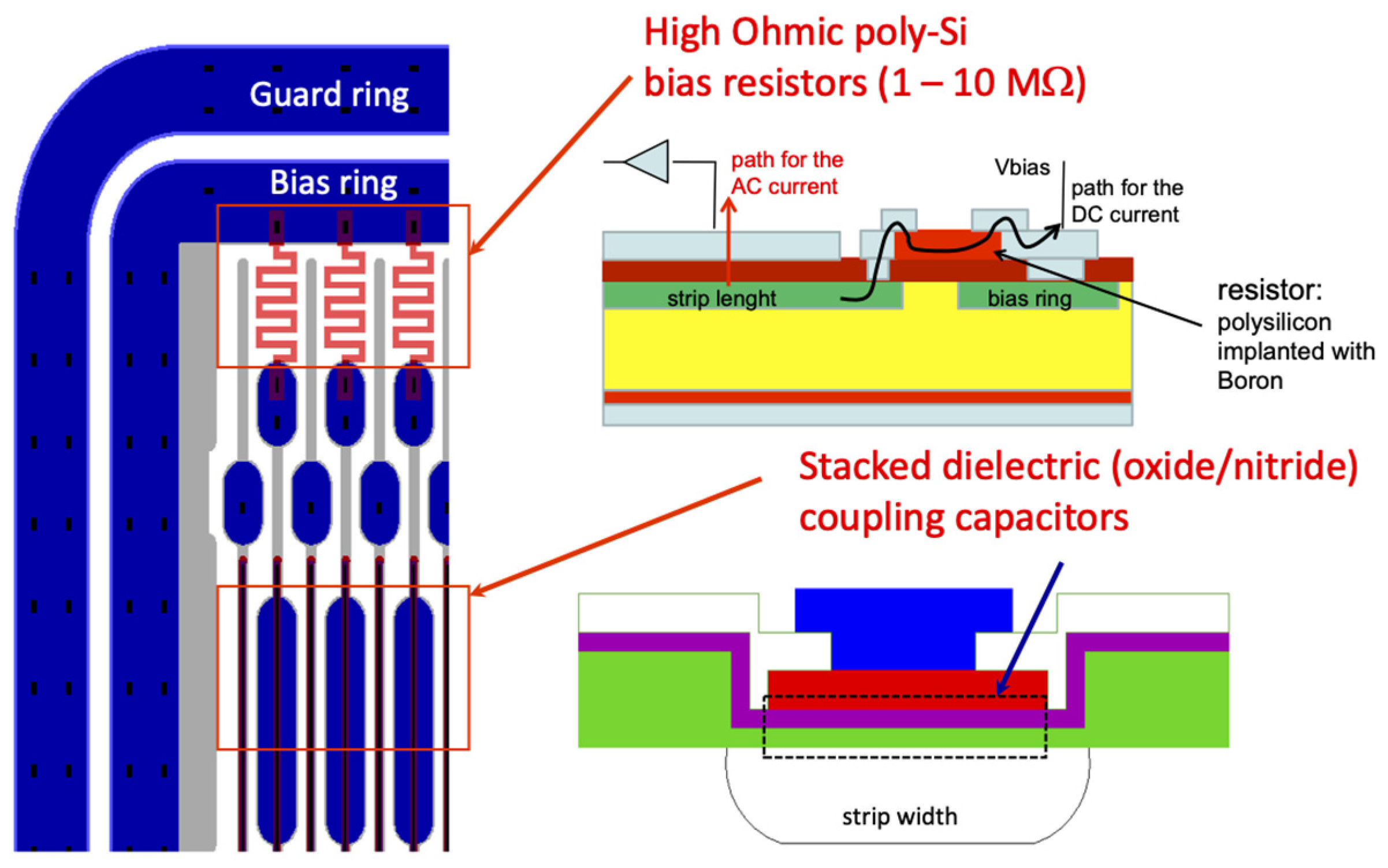
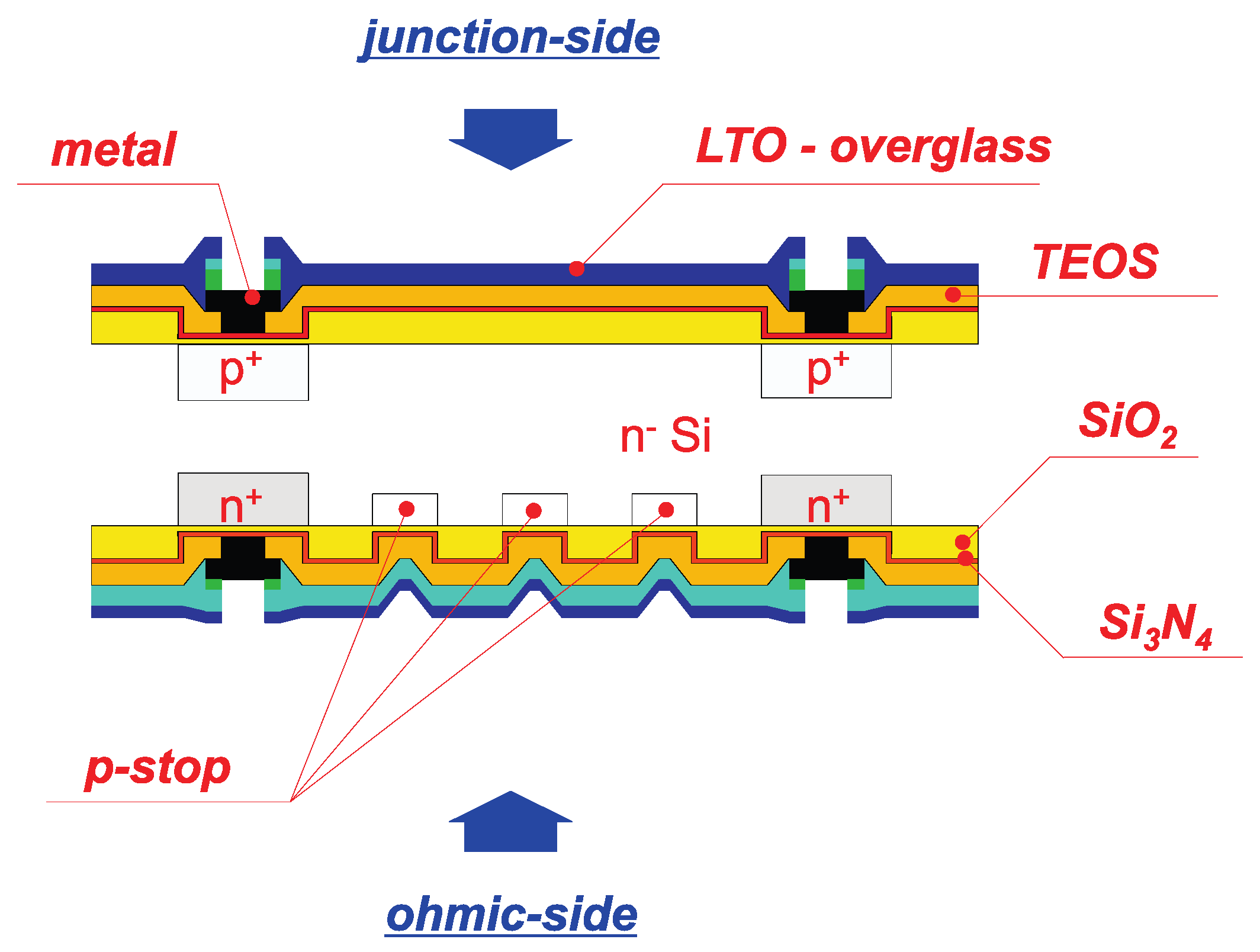
- Only one thermal oxidation step is initially performed at high temperature (~1000 °C) to passivate the silicon surface, creating an effective protection against contamination and mechanical damage and reducing the interface states that are responsible for surface leakage currents. Further oxide layers are then obtained by chemical vapor deposition (CVD), which can be performed at lower temperatures; as an example, the decomposition of the vapor produced from a liquid source, tetraethylorthosilicate (TEOS), is used in a low-pressure (LP) CVD system at about 800 °C (). If a silicon dioxide film is required over aluminum metallization (e.g., for final passivation), the deposition has to be performed at a temperature below the silicon–aluminum eutectic point (577 °C). For this purpose, low-temperature oxides (LTOs) can be deposited from the reaction between silane and oxygen at temperatures between 300 and 500 °C in an LPCVD system (). As an alternative, oxide layers can also be deposited by plasma-enhanced CVD (PECVD) at a typical temperature of 300 °C (. CVD reactions at relatively low temperatures (from ~600 to ~800 °C) are also used for the deposition of poly-Si and silicon nitride;
- -
- the doping of junctions and ohmic contacts is preferably performed by ion implantation, so as to keep the temperature low. The annealing step is also performed at a low temperature (600–700 °C), which is enough for the implant damage recovery, although it does not allow for a full electrical activation of the dopant atoms.
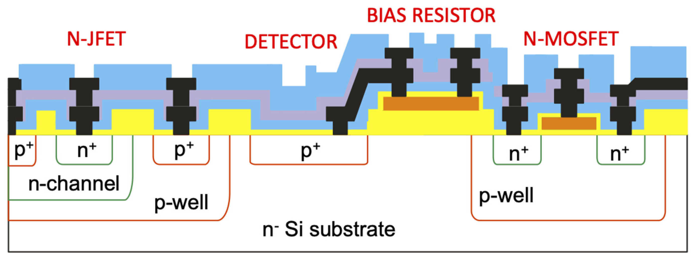
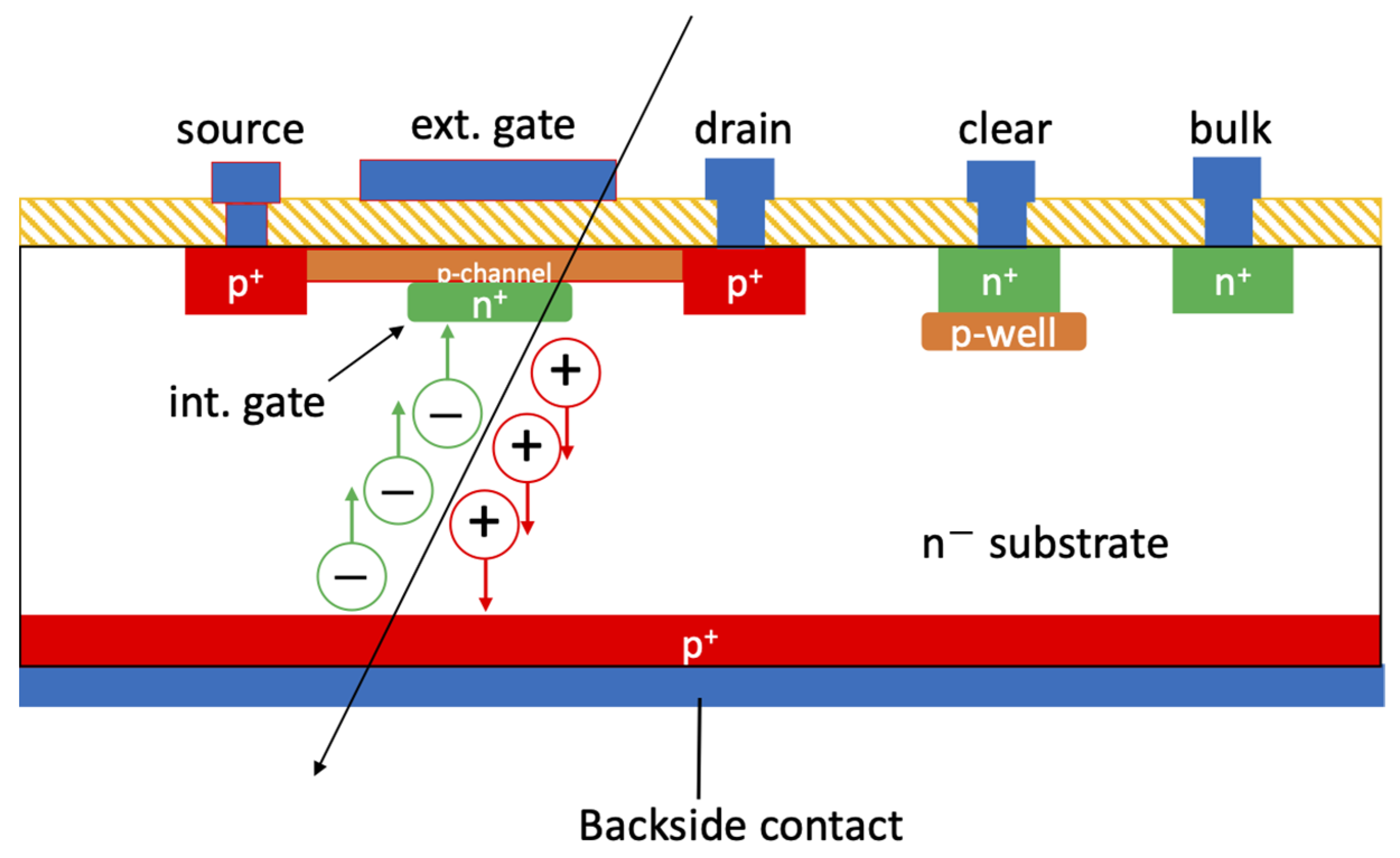
3.2.3. Integrated Transistors
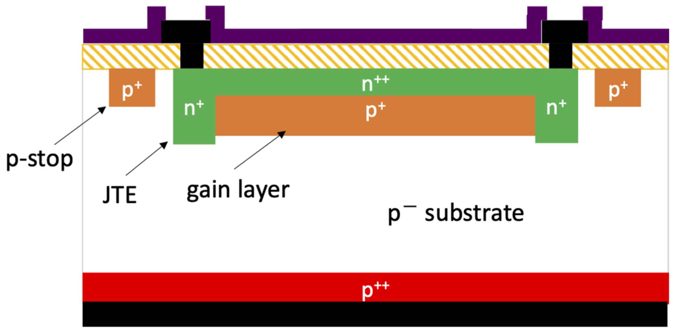
3.2.4. Avalanche-Based Detectors
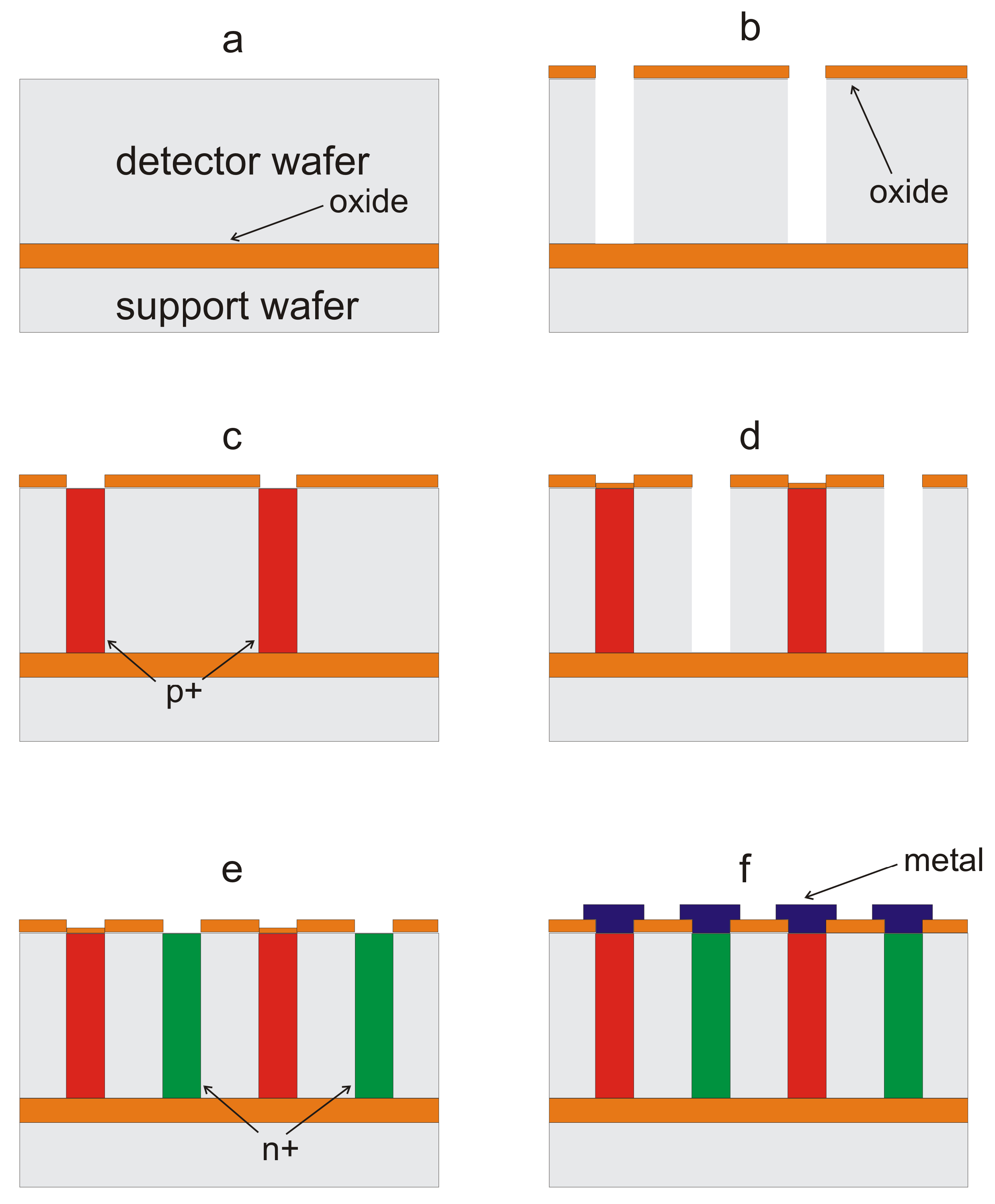
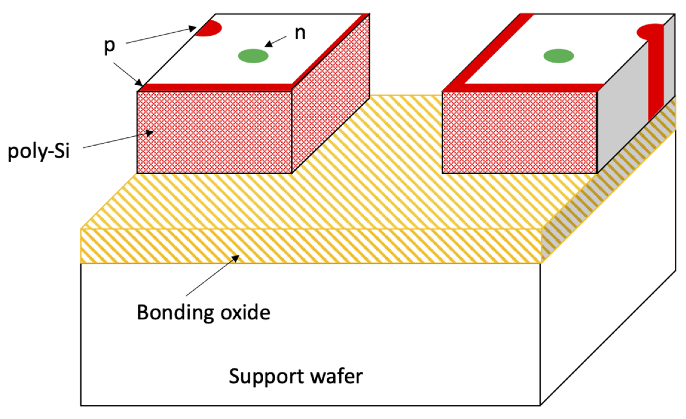
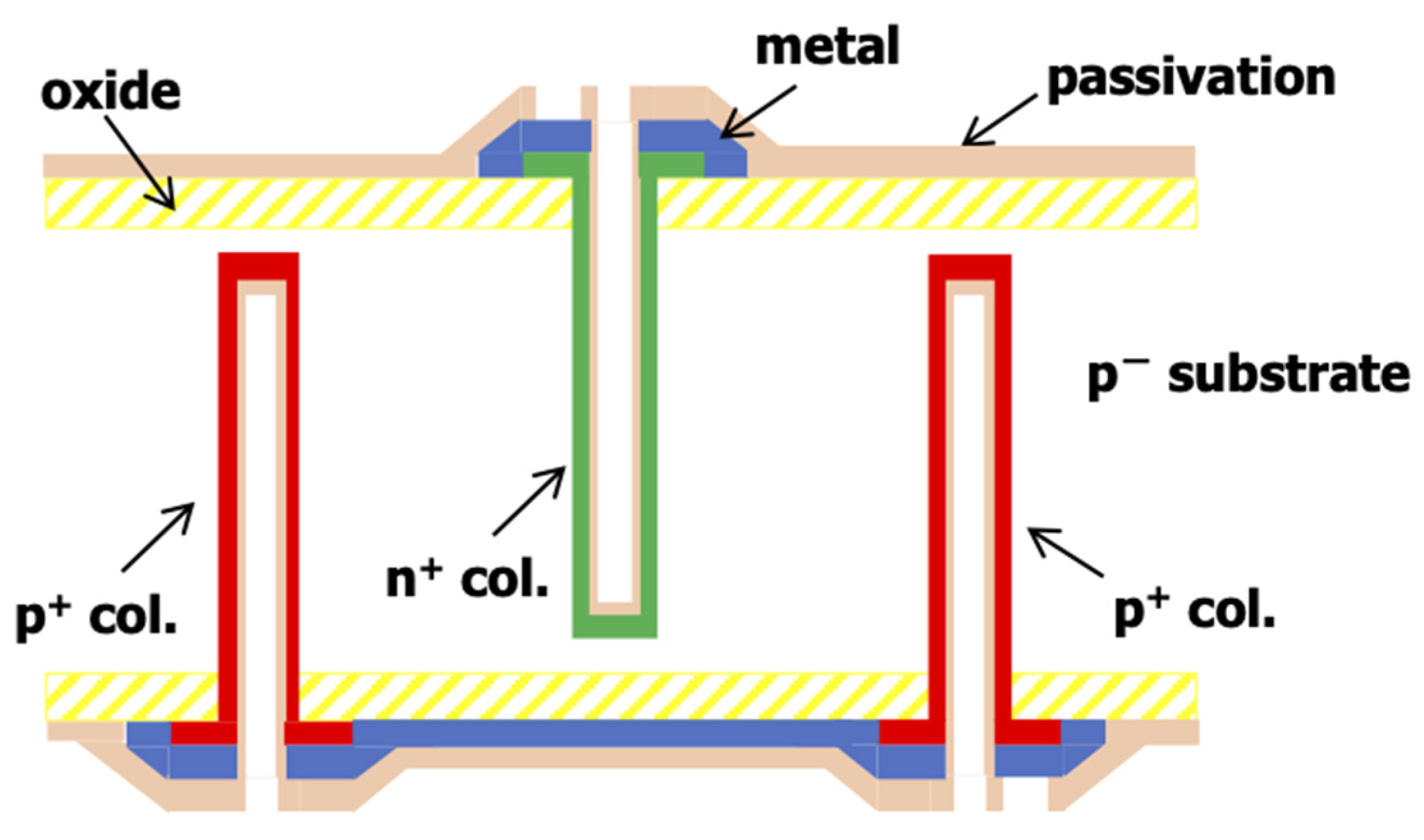
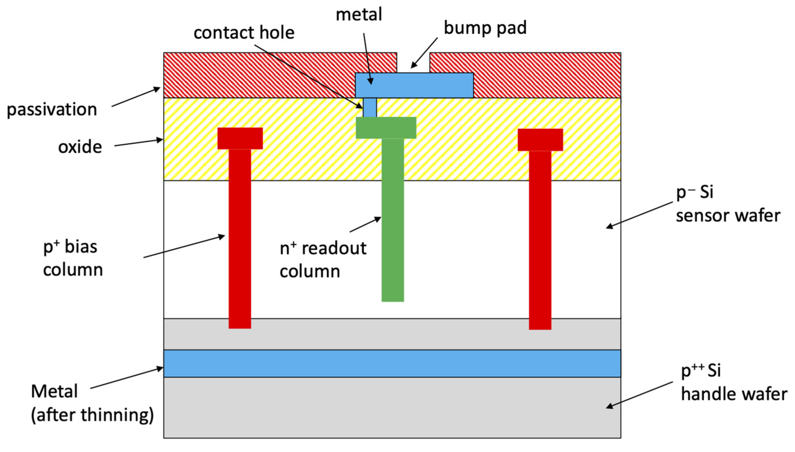
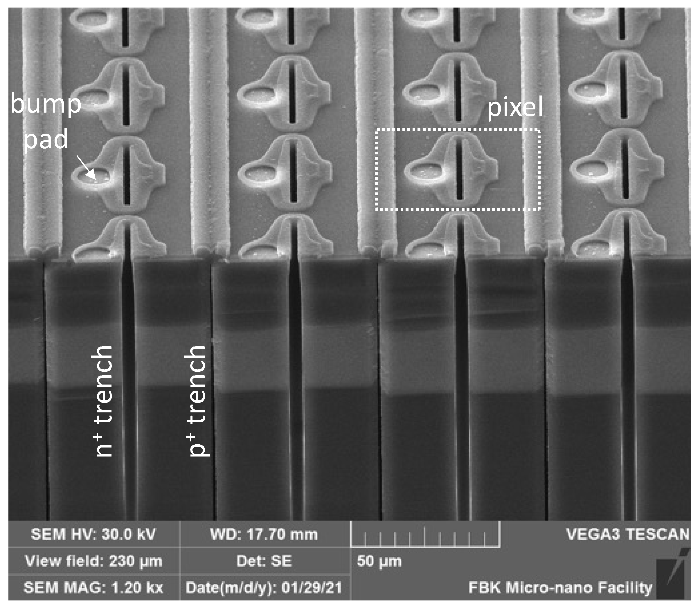
3.3. 3D Technology
- (i)
- The full depletion voltage is much lower: before irradiation, a 3D detector can be efficiently operated at a bias of just a few Volts, and even after irradiation up to very large fluences of the order of ~1016 neq/cm2, the required bias voltage is still limited to ~150 V. Since the leakage current after irradiation can become very large, the related reduction in the power dissipation is very important;
- (ii)
- The time response is much faster: the total signal duration is typically below 1 ns, with rise times below 100 ps, leading to outstanding results in the timing resolution (a few tens of ps);
- (iii)
- Charge-trapping effects, which represent the most important limitation to the signal efficiency after large irradiation fluences, can be strongly attenuated, making 3D detectors the most radiation-hard silicon detectors;
- (iv)
- The extension of the dead region at the detector periphery, which in planar detectors is typically a few hundreds of micrometers, can be minimized to just a few μm by using deep trench terminations, the so-called “active edges”;
- (v)
- Three-dimensional structures with high aspect-ratio cavities filled by proper converter materials (e.g., 6LiF or 10B) can be used for thermal neutron detection and imaging with high efficiency, up to ~50%, owing to the increased surface area of the silicon sensors where the neutron converter material is deposited [81,82,83,84];
- (vi)
- Very small detection volumes can be accurately defined in 3D structures, as requested for microdosimetry in synchrotron and particle therapy and space radiation protection [85].
4. Conclusions
Author Contributions
Funding
Institutional Review Board Statement
Informed Consent Statement
Data Availability Statement
Acknowledgments
Conflicts of Interest
References
- Knoll, G.F. Radiation Detection and Measurement, 4th ed.; Wiley: New York, NY, USA, 2010. [Google Scholar]
- Lutz, G. Semiconductor Radiation Detectors–Device Physics, 2nd ed.; Springer: Berlin/Heidelberg, Germany, 2007. [Google Scholar]
- Marco-Hernández, R. Overview of CMOS sensors for future tracking detectors. Instruments 2020, 4, 36. [Google Scholar] [CrossRef]
- Ramo, S. Currents induced by electron motion. Proc. IRE 1939, 27, 584–585. [Google Scholar] [CrossRef]
- Goulding, F.S.; Hansen, W.L. Leakage current in semiconductor junction radiation detectors and its influence on energy-resolution characteristics. Nuclear Instrum. Methods 1961, 12, 249–262. [Google Scholar] [CrossRef]
- Da Rold, M.; Bacchetta, N.; Bisello, D.; Paccagnella, A.; Dalla Betta, G.F.; Verzellesi, G.; Verdini, P.G. Study of breakdown effects in silicon multiguard structures. IEEE Trans. Nucl. Sci. 1999, 46, 1215–1223. [Google Scholar] [CrossRef]
- Moll, M. Displacement Damage in Silicon Detectors for High Energy Physics. IEEE Trans. Nucl. Sci. 2018, 65, 1561–1582. [Google Scholar] [CrossRef]
- Ma, T.P.; Dressendorfer, P.V. Ionizing Radiation Effects in MOS Devices and Circuits, 1st ed.; Wiley: New York, NY, USA, 1989. [Google Scholar]
- Zhang, J.; Fretwurst, E.; Klanner, R.; Pintilie, I.; Schwandt, J.; Turcato, M. Investigation of X-ray induced radiation damage at the Si-SiO2 interface of silicon sensors for the European XFEL. J. Instrum. 2012, 7, C12012. [Google Scholar] [CrossRef]
- Von Ammon, W.; Herzer, H. The production and availability of high resistivity silicon for detector applications. Nuclear Instrum. Methods 1984, 226, 94–102. [Google Scholar] [CrossRef]
- Dreier, P. High resistivity silicon for detector applications. Nuclear Instrum. Methods 1990, 288, 272–277. [Google Scholar] [CrossRef]
- Lindström, G.; Moll, M.; Fretwurst, E. The RD48 Collaboration. Radiation hardness of silicon detectors–A challenge from high energy physics. Nuclear Instrum. Methods A 2001, 426, 1–15. [Google Scholar] [CrossRef]
- Seidel, S. Silicon strip and pixel detectors for particle physics experiments. Phys. Rep. 2019, 828, 1–34. [Google Scholar] [CrossRef]
- Landi, G.; Landi, G.E. Silicon micro-strip detectors. Encyclopedia 2021, 1, 1076–1083. [Google Scholar] [CrossRef]
- Straver, J.; Toker, O.; Weilhammer, P.; Colledani, C.; Dulinski, W.; Turchetta, R.; Bosisio, L. One micron spatial resolution with silicon strip detectors. Nuclear Instrum. Methods A 1994, 348, 485–490. [Google Scholar] [CrossRef]
- Batignani, G.; Bosi, F.; Bosisio, L.; Conti, A.; Focardi, E.; Forti, F.; Giorgi, M.; Parrini, G.; Scarlini, E.; Tempesta, P.; et al. Double-sided readout silicon strip detectors for the ALEPH minivertex. Nuclear Instrum. Methods A 1989, 277, 147–153. [Google Scholar] [CrossRef]
- Unno, Y.; Abo, Y.; Affolder, A.; Allport, P.; Bloch, I.; Blue, A.; Fadeyev, V.; Fernandez-Tejero, J.; Gregor, I.; Haber, C.; et al. ATLAS17LS–A large-format prototype silicon strip sensor for long-strip barrel section of ATLAS ITk strip detector. Nuclear Instrum. Methods 2021, 989, 164928. [Google Scholar] [CrossRef]
- Bergauer, T.; Dragicevic, M.; König, A.; Hacker, J.; Bartl, U. First thin AC-coupled silicon strip sensors on 8-inch wafers. Nuclear Instrum. Methods 2016, 830, 473–479. [Google Scholar] [CrossRef]
- Riedler, P.; Anelli, G.; Antinori, F.; Badalà, A.; Bruno, G.; Burns, M.; Cali, I.; Campbell, M.; Caselle, M.; Ceresa, S.; et al. Production and Integration of the ALICE Silicon Pixel Detector. Nuclear Instrum. Methods 2007, 572, 128–131. [Google Scholar] [CrossRef]
- Pitzl, D.; Cartiglia, N.; Hubbard, B.; Hutchinson, D.; Leslie, J.; O’Shaughnessy, K.; Rowe, W.; Sadrozinski, H.-W.; Seiden, A.; Spencer, E.; et al. Type inversion in silicon detectors. Nuclear Instrum. Methods 1992, 311, 98–104. [Google Scholar] [CrossRef]
- Affolder, A.; Allport, P.; Casse, G. Charge Collection Efficiency measurements of heavily irradiated segmented n-in-p and p-in-n silicon detectors for use at the Super-LHC. IEEE Trans. Nucl. Sci. 2009, 56, 765–770. [Google Scholar] [CrossRef]
- Affolder, A.; Allport, P.; Casse, G. Charge collection efficiencies of planar silicon detectors after reactor neutron and proton doses up to 1.6 × 10¹⁶ neq cm−2. Nuclear Instrum. Methods 2010, 612, 470–473. [Google Scholar] [CrossRef]
- Hügging, F.; Gößling, C.; Klaiber-Lodewigs, J.; Wüstenfeld, J.; Wunstorf, R. Prototype performance and design of the ATLAS pixel sensors. Nucl. Instrum. Methods 2001, 465, 77–82. [Google Scholar] [CrossRef]
- Allkofer, Y.; Amsler, C.; Bortoletto, D.; Chiochia, V.; Cremaldi, L.; Cucciarelli, S.; Dorokhov, A.; Hörmann, C.; Horisberger, R.; Kim, D.; et al. Design and performance of the silicon sensors for the CMS barrel pixel detector. Nucl. Instrum. Methods 2008, 584, 25–41. [Google Scholar] [CrossRef]
- Rossi, L.; Fischer, P.; Rohe, T.; Wermes, N. Pixel Detectors–From Fundamentals to Applications, 1st ed.; Springer: Berlin-Heidelberg, Germany, 2006. [Google Scholar]
- Battaglia, M.; Da Viá, C.; Bortoletto, D.; Brenner, R.; Campbell, M.; Collins, P.; Dalla Betta, G.-F.; Demarteau, M.; Denes, P.; Graafsma, H.; et al. R&D paths of pixel detectors for vertex tracking and radiation imaging. Nucl. Instrum. Methods 2013, 716, 29–45. [Google Scholar]
- Gatti, E.; Rehak, P. Semiconductor drift chamber-an application of a novel charge transport scheme. Nucl. Instrum. Methods 1984, 225, 608–614. [Google Scholar] [CrossRef]
- Gatti, E.; Rehak, P.; Walton, J. Silicon drift chambers-first results and optimum processing of the signal. Nucl. Instrum. Methods 1984, 226, 129–141. [Google Scholar] [CrossRef]
- Rehak, P.; Gatti, E.; Longoni, A.; Kemmer, J.; Holl, P.; Klanner, R.; Lutz, G.; Wylie, A. Semiconductor drift chambers for position and energy measurements. Nucl. Instrum. Methods 1985, 235, 224–234. [Google Scholar] [CrossRef]
- Hartmann, R.; Strüder, L.; Kemmer, J.; Lechner, P.; Fries, O.; Lorenz, E.; Mirzoyan, R. Ultrathin entrance windows for silicon drift detectors. Nucl. Instrum. Methods 1997, 387, 250–254. [Google Scholar] [CrossRef]
- Segal, J.; Kenney, C.; Kowalski, J.M.; Blaj, G.; Rozario, L.; Hasi, J.; Dragone, A.; Caragiulo, P.; Rota, L. Thin-entrance window process for soft X-ray sensors. Front. Phys. 2021, 9, 618390. [Google Scholar] [CrossRef]
- Bertuccio, G.; Ahangarianabhari, M.; Graziani, C.; Macera, D.; Shi, Y.; Gandola, M.; Rachevski, A.; Rashevskaya, I.; Vacchi, A.; Zampa, G.; et al. X-ray Silicon Drift Detector–CMOS front-end system with high energy resolution at room temperature. IEEE Trans. Nucl. Sci. 2016, 63, 400–406. [Google Scholar] [CrossRef]
- Rehak, P.; Gatti, E.; Longoni, A.; Sampietro, M.; Holl, P.; Lutz, G.; Kemmer, J.; Prechtel, U.; Ziemann, T. Spiral silicon drift detectors. IEEE Trans. Nucl. Sci. 1989, 36, 203–209. [Google Scholar] [CrossRef]
- Rashevsky, A.; Bonvicini, V.; Vacchi, A.; Zampa, N.; Burger, P.; Beole, S.; Idzik, M.; Petta, C.; Randazzo, N. Silicon drift detector with a continuous implanted resistor as divider-drift electrode. Nucl. Instrum. Methods 1998, 409, 210–215. [Google Scholar] [CrossRef]
- Jiang, S.; Jia, R.; Tao, K.; Wu, Y.; Liu, S. High-resistance voltage dividers fabricated by thin polysilicon films in silicon drift detectors. J. Mater. Sci. Mater. Electron. 2019, 30, 6617–6627. [Google Scholar] [CrossRef]
- Kemmer, J. Fabrication of low noise silicon radiation detectors by the planar process. Nucl. Instrum. Methods 1980, 169, 499–502. [Google Scholar] [CrossRef]
- Kemmer, J.; Burger, P.; Henck, R.; Heijne, E. Performance and applications of passivated ion-implanted silicon detectors. IEEE Trans. Nucl. Sci. 1982, 29, 733–737. [Google Scholar] [CrossRef]
- Kemmer, J. Improvement of detector fabrication by the planar process. Nucl. Instrum. Methods 1984, 226, 89–93. [Google Scholar] [CrossRef]
- Holland, S. An IC compatible detector process. IEEE Trans. Nucl. Sci. 1989, 36, 283–289. [Google Scholar] [CrossRef]
- Dalla Betta, G.; Pignatel, G.; Verzellesi, G.; Boscardin, M. Si-PIN X-ray detector technology. Nucl. Instrum. Methods A 1997, 395, 344–348. [Google Scholar] [CrossRef]
- Caccia, M.; Evensen, L.; Hansen, T.E.; Horisberger, R.; Hubbeling, L.; Peisert, A.; Zalewska, A. A Si strip detector with integrated coupling capacitors. Nucl. Instrum. Methods 1987, 260, 124–131. [Google Scholar] [CrossRef]
- Dalla Betta, G.-F.; Boscardin, M.; Bosisio, L. A comparative evaluation of integrated capacitors for AC-coupled microstrip detectors. Nucl. Instrum. Methods A 1998, 411, 369–375. [Google Scholar] [CrossRef]
- Hietanen, I.; Lindgren, J.; Orava, R.; Tuuva, T.; Voutilainen, M.; Brenner, R.; Andersson, M.; Leinonen, K.; Ronkainen, H. Ion-implanted capacitively coupled silicon strip detectors with integrated polysilicon bias resistors processed on a 100 mm wafer. Nucl. Instrum. Methods A 1991, 310, 671–676. [Google Scholar] [CrossRef]
- Dalla Betta, G.-F.; Boscardin, M.; Bosisio, L.; Rachevskaia, I.; Zen, M.; Zorzi, N. Development of a fabrication technology for double-sided AC-coupled silicon microstrip detectors. Nucl. Instrum. Methods 2001, 460, 306–315. [Google Scholar] [CrossRef]
- Iwata, Y.; Ohsugi, T.; Fujita, K.; Kitabayashi, H.; Yamamoto, K.; Yamamura, K.; Unno, Y.; Kondo, T.; Terada, S.; Kohriki, T.; et al. Optimal p-stop pattern for the n-side strip isolation of silicon microstrip detectors. IEEE Trans. Nucl. Sci. 1998, 45, 303–309. [Google Scholar] [CrossRef]
- Richter, R. Strip detector design for ATLAS and HERA-B using two-dimensional device simulation. Nucl. Instrum. Methods 1996, 377, 412–421. [Google Scholar] [CrossRef]
- Piemonte, C. Device simulations of isolation techniques for silicon microstrip detectors made on p-type substrates. IEEE Trans. Nucl. Sci. 2006, 53, 1694–1705. [Google Scholar] [CrossRef]
- Holland, S. Properties of CMOS devices and circuits fabricated on high-resistivity, detector-grade silicon. IEEE Trans. Nucl. Sci. 1992, 39, 809–813. [Google Scholar] [CrossRef]
- Radeka, V.; Rahek, P.; Rescia, S.; Gatti, E.; Longoni, A.; Sampietro, M.; Bertuccio, G.; Holl, P.; Struder, L.; Kemmer, J. Implanted silicon JFET on completely depleted high-resistivity devices. IEEE Electron. Device Lett. 1989, 10, 91–94. [Google Scholar] [CrossRef]
- Rehak, P.; Rescia, S.; Radeka, V.; Gatti, E.; Longoni, A.; Sampietro, M.; Bertuccio, G.; Holl, P.; Strüder, L.; Kemmer, J.; et al. Feedback charge amplifier integrated on detector wafer. Nucl. Instrum. Methods A 1990, 288, 168–175. [Google Scholar] [CrossRef]
- Sampietro, M.; Fasoli, L.; Rehak, P.; Struder, L. Novel p-JFET embedded in silicon radiation detectors avoids preamplifier feedback resistor. IEEE Electron. Device Lett. 1995, 16, 208–210. [Google Scholar] [CrossRef]
- Dalla Betta, G.-F.; Boscardin, M.; Gregori, P.; Zorzi, N.; Pignatel, G.; Batignani, G.; Giorgi, M.; Bosisio, L.; Ratti, L.; Speziali, V.; et al. A fabrication process for silicon microstrip detectors with integrated front-end electronics. IEEE Trans. Nucl. Sci. 2002, 49, 1022–1026. [Google Scholar] [CrossRef]
- Dalla Betta, G.-F.; Batignani, G.; Boscardin, M.; Bosisio, L.; Gregori, P.; Pancheri, L.; Piemonte, C.; Ratti, L.; Verzellesi, G.; Zorzi, N. Monolithic integration of detectors and transistors on high-resistivity silicon. Nucl. Instrum. Methods A 2007, 579, 658–663. [Google Scholar] [CrossRef]
- Dalla Betta, G.-F.; Boscardin, M.; Fenotti, F.; Pancheri, L.; Piemonte, C.; Ratti, L.; Zorzi, N. Low noise Junction Field Effect Transistors in a silicon radiation detector technology. IEEE Trans. Nucl. Sci. 2006, 53, 3004–3012. [Google Scholar] [CrossRef]
- Bosisio, L.; Batignani, G.; Bettarini, S.; Boscardin, M.; Dalla Betta, G.-F.; Giacomini, G.; Piemonte, C.; Verzellesi, G.; Zorzi, N. Performance evaluation of radiation sensors with internal signal amplification based on the BJT effect. Nucl. Instrum. Methods 2006, 568, 217–223. [Google Scholar] [CrossRef]
- Rovati, L.; Bettarini, S.; Bonaiuti, M.; Bosisio, L.; Dalla Betta, G.-F.; Tyzhnevyi, V.; Verzellesi, G.; Zorzi, N. Alpha-particle detection based on the BJT detector and simple, IC-based readout electronics. J. Instrum. 2009, 4, P11010. [Google Scholar] [CrossRef]
- Kemmer, J.; Lutz, G. New detector concepts. Nucl. Instrum. Methods 1987, 253, 365–377. [Google Scholar] [CrossRef]
- Lutz, G. DEPFET development at the MPI semiconductor laboratory. Nuclear Instrum. Methods 2005, 549, 103–111. [Google Scholar] [CrossRef]
- Wolfel, S.; Herrmann, S.; Lechner, P.; Lutz, G.; Porro, M.; Richter, R.H.; Treis, J. A novel way of single optical photon detection: Beating the 1/f noise limit with ultra-high resolution DEPFET-RNDR devices. IEEE Trans. Nucl. Sci. 2007, 54, 1311–1318. [Google Scholar] [CrossRef]
- Lutz, G.; Lechner, P.; Porro, M.; Strüder, L.; De Vita, G. DEPFET sensor with intrinsic signal compression developed for use at the XFEL free electron laser radiation source. Nucl. Instrum. Methods 2010, 624, 528–532. [Google Scholar] [CrossRef]
- Andricek, L.; Bähr, A.; Lechner, P.; Ninkovic, J.; Richter, R.; Schopper, F.; Treis, J. DePFET–Recent developments and future prospects. Front. Phys. 2022, 10, 896212. [Google Scholar] [CrossRef]
- Giacomini, G. LGAD-Based Silicon Sensors for 4D Detectors. Sensors 2023, 23, 2132. [Google Scholar] [CrossRef]
- Cartiglia, N.; Staiano, A.; Sola, V.; Arcidiacono, R.; Cirio, R.; Cenna, F.; Ferrero, M.; Monaco, V.; Mulargia, R.; Obertino, M.; et al. Beam test results of a 16 ps timing system based on ultra-fast silicon detectors. Nucl. Instrum. Methods 2017, 850, 83–88. [Google Scholar] [CrossRef]
- McIntyre, R.J. Multiplication noise in uniform avalanche diodes. IEEE Trans. Electron. Dev. 1966, 13, 164–168. [Google Scholar] [CrossRef]
- Ferrero, M.; Arcidiacono, R.; Mandurrino, M.; Sola, V.; Cartiglia, N. An Introduction to Ultra-Fast Silicon Detectors, 1st ed.; CRC Press: Boca Raton, FL, USA, 2021. [Google Scholar]
- Pellegrini, G.; Fernández-Martínez, P.; Baselga, M.; Fleta, C.; Flores, D.; Greco, V.; Hidalgo, S.; Mandić, I.; Kramberger, G.; Quirion, D.; et al. Technology developments and first measurements of Low Gain Avalanche Detectors (LGAD) for high energy physics applications. Nucl. Instrum. Methods A 2014, 765, 12–16. [Google Scholar] [CrossRef]
- Giacomini, G. Fabrication of Silicon Sensors Based on Low-Gain Avalanche Diodes. Front. Phys. 2021, 9, 618621. [Google Scholar] [CrossRef]
- Cartiglia, N.; Arcidiacono, R.; Ferrero, M.; Mandurrino, M.; Sadrozinski, H.-F.; Sola, V.; Staiano, A.; Seiden, A. Timing layers: 4- and 5-dimensions tracking. Nucl. Instrum. Methods 2019, 924, 350–354. [Google Scholar] [CrossRef]
- Dall Betta, G.-F.; Pancheri, L.; Boscardin, M.; Paternoster, G.; Piemonte, C.; Cartiglia, N.; Cenna, F.; Bruzzi, M. Design and TCAD simulation of double-sided pixelated low gain avalanche detectors. Nucl. Instrum. Methods 2015, 796, 154–157. [Google Scholar] [CrossRef]
- Currás, E.; Carulla, M.; Vignali, M.C.; Duarte-Campderros, J.; Fernández, M.; Flores, D.; García, A.; Gómez, G.; González, J.; Hidalgo, S.; et al. Inverse Low Gain Avalanche Detectors. iLGADs) for precise tracking and timing applications. Nucl. Instrum. Methods A 2020, 958, 162545. [Google Scholar] [CrossRef]
- Giacomini, G.; Chen, W.; D’Amen, G.; Tricoli, A. Fabrication and performance of AC-coupled LGADs. J. Instrum. 2019, 14, P09004. [Google Scholar] [CrossRef]
- Mandurrino, M.; Arcidiacono, R.; Boscardin, M.; Cartiglia, N.; Dalla Betta, G.F.; Ferrero, M.; Ficorella, F.; Pancheri, L.; Paternoster, G.; Siviero, F.; et al. Tornago, M. Demonstration of 200-, 100-, and 50-mm pitch Resistive AC-coupled Silicon Detectors. RSD) with 100% fill-factor for 4D particle tracking. IEEE Electron. Device Lett. 2019, 40, 1780–1783. [Google Scholar] [CrossRef]
- Menzio, L.; Arcidiacono, R.; Borghi, G.; Boscardin, M.; Cartiglia, N.; Vignali, M.C.; Costa, M.; Dall Betta, G.-F.; Ferrero, M.; Ficorella, F.; et al. DC-coupled resistive silicon detectors for 4D tracking. Nucl. Instrum. Methods A 2022, 1041, 167374. [Google Scholar] [CrossRef]
- Paternoster, G.; Borghi, G.; Boscardin, M.; Cartiglia, N.; Ferrero, M.; Ficorella, F.; Siviero, F.; Gola, A.; Bellutti, P. Trench-Isolated low gain avalanche diodes. TI-LGADs. IEEE Electron. Device Lett. 2020, 41, 884–887. [Google Scholar] [CrossRef]
- Kramberger, G.; Baselga, M.; Cindro, V.; Fernández-Martínez, P.; Flores, D.; Galloway, Z.; Gorišek, A.; Greco, V.; Hidalgo, S.; Fadeyev, V.; et al. Radiation effects in Low Gain Avalanche Detectors after hadron irradiations. J. Instrum. 2015, 10, P07006. [Google Scholar] [CrossRef]
- Ferrero, M.; Arcidiacono, R.; Barozzi, M.; Boscardin, M.; Cartiglia, N.; Dalla Betta, G.; Galloway, Z.; Mandurrino, M.; Mazza, S.; Paternoster, G.; et al. Radiation resistant LGAD design. Nucl. Instrum. Methods 2019, 919, 16–26. [Google Scholar] [CrossRef]
- Li, M.; Fan, Y.; Jia, X.; Cui, H.; Liang, Z.; Zhao, M.; Yang, T.; Wu, K.; Li, S.; Yu, C.; et al. Effects of shallow carbon and deep N++ layer on the radiation hardness of IHEP-IME LGAD sensors. IEEE Trans. Nucl. Sci. 2022, 69, 1098–1103. [Google Scholar] [CrossRef]
- Andrä, M.; Zhang, J.; Bergamaschi, A.; Barten, R.; Borca, C.; Borghi, G.; Boscardin, M.; Busca, P.; Brückner, M.; Cartiglia, N.; et al. Development of low-energy X-ray detectors using LGAD sensors. J. Synchrotron. Rad. 2019, 26, 1226–1237. [Google Scholar] [CrossRef] [PubMed]
- Zhang, J.; Barten, R.; Baruffaldi, F.; Bergamaschi, A.; Borghi, G.; Boscardin, M.; Thattil, D. Development of LGAD sensors with a thin entrance window for soft X-ray detection. J. Instrum. 2022, 17, C11011. [Google Scholar] [CrossRef]
- Parker, S.I.; Kenney, C.J.; Segal, J. 3D-A proposed new architecture for solid-state radiation detectors. Nucl. Instrum. Methods A 1997, 395, 328–343. [Google Scholar] [CrossRef]
- Bellinger, S.L.; Fronk, R.G.; McNeil, W.J.; Sobering, T.J.; McGregor, D.S. Improved high efficiency stacked microstructured neutron detectors backfilled with nanoparticle 6LiF. IEEE Trans. Nucl. Sci. 2012, 59, 167–173. [Google Scholar] [CrossRef]
- Kok, A.; Kohout, Z.; Hansen, T.E.; Petersson, S.; Pospisil, S.; Rokne, J.; Vykydal, Z. Silicon sensors with pyramidal structures for neutron imaging. J. Instrum. 2014, 9, C04011. [Google Scholar] [CrossRef]
- Mendicino, R.; Dalla Betta, G.F. Three-Dimensional detectors for neutron imaging. Nucl. Instrum. Methods A 2018, 878, 129–140. [Google Scholar] [CrossRef]
- Povoli, M.; Kok, A.; Koybasi, O.; Getz, M.; O’Neill, G.; Roehrich, D.; Jansa, I.L. 3D silicon detectors for neutron imaging applications. J. Instrum. 2023, 18, C01056. [Google Scholar] [CrossRef]
- Tran, L.T.; Prokopovich, D.A.; Petasecca, M.; Lerch, M.L.F.; Kok, A.; Summanwar, A.; Hansen, T.-E.; Da Via, C.; Reinhard, M.I.; Rosenfeld, A.B. 3D radiation detectors: Charge collection characterisation and applicability of technology for microdosimetry. IEEE Trans. Nucl. Sci. 2014, 61, 1537–1543. [Google Scholar] [CrossRef]
- Da Vià, C.; Dalla Betta, G.F.; Parker, S. Radiation Sensors with Three-Dimensional Electrodes, 1st ed.; CRC Press: Boca Raton, FL, USA, 2019. [Google Scholar]
- Dalla Betta, G.-F.; Povoli, M. Progress in 3D silicon radiation detectors. Front. Phys. 2022, 10, 927690. [Google Scholar] [CrossRef]
- Laermer, F.; Franssila, S.; Sainiemi, L.; Kolari, K. Deep reactive Ion etching. In Handbook of Silicon Based MEMS Materials and Technologies, 2nd ed.; Tilli, M., Motooka, T., Airaksinen, V.-M., Franssila, S., Kröckel, M.P., Lindroos, V., Eds.; Elsevier Inc.: San Diego, CA, USA, 2015. [Google Scholar] [CrossRef]
- Kenney, C.; Parker, S.; Segal, J.; Storment, C. Silicon Detectors with 3-D Electrode Arrays: Fabrication and Initial Test Results. IEEE Trans. Nucl. Sci. 1999, 46, 1224–1236. [Google Scholar] [CrossRef]
- Christiansen, S.H.; Singh, R.; Gosele, U. Wafer direct bonding: From advanced substrate engineering to future applications in micro/nanoelectronics. IEEE 2006, 94, 2060–2106. [Google Scholar] [CrossRef]
- Kenney, C.; Parker, S.; Walckiers, E. Results from 3-D silicon sensors with wall electrodes: Near-cell-edge sensitivity measurements as a preview of active-edge sensors. IEEE Trans. Nucl. Sci. 2001, 48, 2405–2410. [Google Scholar] [CrossRef]
- Kenney, C.; Segal, J.; Westbrook, E.; Parker, S.; Hasi, J.; Da Via, C.; Watts, S.; Morse, J. Active-edge planar radiation sensors. Nucl. Instrum. Methods A 2006, 565, 272–277. [Google Scholar] [CrossRef] [PubMed]
- Wu, X.; Kalliopuska, J.; Eränen, S.; Virolainen, T. Recent advances in processing and characterization of edgeless detectors. J. Instrum. 2012, 7, C02001. [Google Scholar] [CrossRef]
- Koybasi, O.; Zhang, J.; Kok, A.; Summanwar, A.; Povoli, M.; Breivik, L.; Schmitt, B. Edgeless sensors fabricated without support wafer. Nucl. Instrum. Meth. 2020, 953, 163176. [Google Scholar] [CrossRef]
- Pellegrini, G.; Lozano, M.; Ullán, M.; Bates, R.; Fleta, C.; Pennicard, D. First double-sided 3-D detectors fabricated at CNM-IMB. Nucl. Instrum. Methods A 2008, 592, 38–43. [Google Scholar] [CrossRef]
- Zoboli, A.; Boscardin, M.; Bosisio, L.; Dalla Betta, G.-F.; Piemonte, C.; Ronchin, S.; Zorzi, N. Double-Sided, Double-Type-Column 3-D Detectors: Design, Fabrication, and Technology Evaluation. IEEE Trans. Nucl. Sci. 2008, 55, 2775–2784. [Google Scholar] [CrossRef]
- Giacomini, G.; Bagolini, A.; Boscardin, M.; Dall Betta, G.-F.; Mattedi, F.; Povoli, M.; Vianello, E.; Zorzi, N. Development of double-sided full-passing-column 3D Sensors at FBK. IEEE Trans. Nucl. Sci. 2013, 60, 2357–2366. [Google Scholar] [CrossRef]
- Da Via, C.; Boscardin, M.; Dall Betta, G.-F.; Darbo, G.; Fleta, C.; Gemme, C.; Grenier, P.; Grinstein, S.; Hansen, T.-E.; Hasi, J.; et al. 3D silicon sensors: Design, large area production and quality assurance for the ATLAS IBL pixel detector upgrade. Nucl. Instrum. Methods A 2012, 694, 321–330. [Google Scholar] [CrossRef]
- Povoli, M.; Bagolini, A.; Boscardin, M.; Dalla Betta, G.-F.; Giacomini, G.; Vianello, E.; Zorzi, N. Slim edges in double-sided silicon 3D detectors. J. Instrum. 2012, 7, C01015. [Google Scholar] [CrossRef]
- Terzo, S.; Boscardin, M.; Carlotto, J.; Dalla Betta, G.F.; Darbo, G.; Dorholt, O.; Vannoli, L. Novel 3D pixel sensors for the upgrade of the ATLAS Inner Tracker. Front. Phys. 2021, 9, 624668. [Google Scholar] [CrossRef]
- Meschini, M.; Cassese, A.; Ceccarelli, R.; Viliani, L.; Dinardo, M.; Gennai, S.; Zuolo, D.; Messineo, A.; Parolia, S.; Ebrahimi, A.; et al. Radiation resistant innovative 3D pixel sensors for the CMS upgrade at the High Luminosity LHC. Nucl. Instrum. Methods 2020, 978, 164429. [Google Scholar] [CrossRef]
- Dalla Betta, G.-F.; Boscardin, M.; Darbo, G.; Mendicino, R.; Meschini, M.; Messineo, A.; Ronchin, S.; Sultan, D.M.S.; Zorzi, N. Development of a new generation of 3D pixel sensors for HL-LHC. Nucl. Instrum. Methods A 2016, 824, 386–387. [Google Scholar] [CrossRef]
- Parker, S.; Kok, A.; Kenney, C.; Jarron, P.; Hasi, J.; Despeisse, M.; Da Via, C.; Anelli, G. Increased speed: 3D silicon sensors; fast current amplifiers. IEEE Trans. Nucl. Sci. 2011, 58, 404–417. [Google Scholar] [CrossRef]
- Mendicino, R.; Forcolin, G.T.; Boscardin, M.; Ficorella, F.; Lai, A.; Loi, A.; Ronchin, S.; Vecchi, S.; Dalla Betta, G.-F. 3D Trenched-Electrode Sensors for Charged Particle Tracking and Timing. Nucl. Instrum. Methods A 2019, 927, 24–30. [Google Scholar] [CrossRef]
- Borgato, F.; Brundu, D.; Cardini, A.; Cossu, G.M.; Dalla Betta, G.F.; Garau, M.; La Delfa, L.; Lai, A.; Lampis, A.; Loi, A.; et al. Charged-particle timing with 10 ps accuracy using TimeSPOT 3D trench-type silicon pixels. Front. Phys. 2023, 11, 1117575. [Google Scholar] [CrossRef]
- Lampis, A.; Borgato, F.; Brundu, D.; Cardini, A.; Cossu, G.M.; Dalla Betta, G.F.; Vecchi, S. 10 ps timing with highly irradiated 3D trench silicon pixel sensors. J. Instrum. 2023, 18, C01051. [Google Scholar] [CrossRef]
- Forcolin, G.; Boscardin, M.; Ficorella, F.; Lai, A.; Loi, A.; Mendicino, R.; Ronchin, S.; Dall Betta, G.-F. 3D trenched-electrode pixel sensors: Design, technology and initial results. Nucl. Instrum. Methods 2020, 981, 164437. [Google Scholar] [CrossRef]
- Boscardin, M.; Ferrari, S.; Ficorella, F.; Lai, A.; Mendicino, R.; Meschini, M.; Ronchin, S.; Samy, A.A.; Dall Betta, G.-F. Advances in 3D Sensor Technology using Stepper Lithography. Front. Phys. 2021, 9, 625275. [Google Scholar] [CrossRef]


Disclaimer/Publisher’s Note: The statements, opinions and data contained in all publications are solely those of the individual author(s) and contributor(s) and not of MDPI and/or the editor(s). MDPI and/or the editor(s) disclaim responsibility for any injury to people or property resulting from any ideas, methods, instructions or products referred to in the content. |
© 2023 by the authors. Licensee MDPI, Basel, Switzerland. This article is an open access article distributed under the terms and conditions of the Creative Commons Attribution (CC BY) license (https://creativecommons.org/licenses/by/4.0/).
Share and Cite
Dalla Betta, G.-F.; Ye, J. Silicon Radiation Detector Technologies: From Planar to 3D. Chips 2023, 2, 83-101. https://doi.org/10.3390/chips2020006
Dalla Betta G-F, Ye J. Silicon Radiation Detector Technologies: From Planar to 3D. Chips. 2023; 2(2):83-101. https://doi.org/10.3390/chips2020006
Chicago/Turabian StyleDalla Betta, Gian-Franco, and Jixing Ye. 2023. "Silicon Radiation Detector Technologies: From Planar to 3D" Chips 2, no. 2: 83-101. https://doi.org/10.3390/chips2020006
APA StyleDalla Betta, G.-F., & Ye, J. (2023). Silicon Radiation Detector Technologies: From Planar to 3D. Chips, 2(2), 83-101. https://doi.org/10.3390/chips2020006