Abstract
In the purpose of enhancing solar cell efficiency and sustainability, zinc selenide (ZnSe) and silicon (Si) play indispensable roles, offering a compelling combination of stability and transparency while also highlighting their abundant availability. This study utilizes the SCAPS_1D tool to explore diverse heterojunction setups, aiming to solve the nuanced correlation between key parameters and photovoltaic performance, therefore contributing significantly to the advancement of sustainable energy solutions. Exploring the performance analysis of heterojunction solar cell configurations employing ZnSe and Si elements, various configurations including SnO2/ZnSe/p_Si/p+_Si, SnO2/CdS/p_Si/p+_Si, TiO2/ZnSe/p_Si/p+_Si, and TiO2/CdS/p_Si/p+_Si are investigated, delving into parameters such as back surface field thickness (BSF), doping concentration, operating temperature, absorber layer properties, electron transport layer properties, interface defects, series and shunt resistance. Among these configurations, the SnO2/ZnSe/p_Si/p+_Si configuration with a doping concentration of 1019 cm−3 and a BSF thickness of 2 μm, illustrates a remarkable conversion efficiency of 22.82%, a short circuit current density (Jsc) of 40.33 mA/cm2, an open circuit voltage (Voc) of 0.73 V, and a fill factor (FF) of 77.05%. Its environmentally friendly attributes position it as a promising contender for advanced photovoltaic applications. This work emphasizes the critical role of parameter optimization in propelling solar cell technologies toward heightened efficiency and sustainability.
1. Introduction
Renewable energy technology is a crucial response to the global challenges posed by climate change and the depletion of fossil fuel resources [1,2]. Photovoltaic (PV) solar cells have played a key role in this shift to a clean, sustainable energy source [3,4,5,6,7]. These devices use the power of sunlight to generate electricity, providing a clean and renewable energy source that can respond to the world’s ever-increasing energy demand while minimizing the environmental impacts of conventional energy sources [8,9,10]. From the multitude of solar cell configurations, the heterojunction solar cell, characterized by its unique material interfaces and advanced design, has been receiving considerable attention due to its impressive efficiency and adaptability [11,12,13].
In this context, materials such as SnO2 (tin–tin oxide), ZnSe (zinc selenide), CdS (cadmium sulfide), and TiO2 (titanium dioxide) are a key factor in the manufacture of high-performance, long-lasting solar cells, with their particular qualities and affinity with modern photovoltaic technologies. Each material contributes to the enhancement of solar cells. SnO2 tin oxide is a transparent material that can be deposited as a thin layer on solar cells to allow sunlight to be transmitted to the active layers [14,15,16,17]. In addition, it is a good electrical conductor, making it easier to collect the electrons generated by the light [18,19]. ZnSe (Zinc Selenide) has an adequate energy gap for use as a buffer layer material or as a junction material in solar cells based in thin-film [20,21,22,23]. It can improve the effective conversion of sunlight to power. On the other hand, CdS is widely employed as a buffer layer in solar cells, as it allows a smooth transition between the absorber layer and the contact layer. It can also help to minimize the reflection of light from the cell surface [24,25,26]. TiO2 is commonly employed as a material for the front electrodes of solar cells, most notably in perovskite and dye-sensitized (DSSCs) solar cells. It promotes the transport of electrons generated by sunlight and can improve conversion efficiency [27,28,29]. However, P_Si and P+_Si layers are crucial for charge carrier transport, surface passivation, and energy band alignment, influencing key parameters such as open circuit voltage (), and power conversion efficiency [30,31,32]. An understanding and optimization of these materials is fundamental to achieving greater energy conversion efficiency and advancing the capabilities of photovoltaic technology. These materials are selected based on their specific properties, such as their band gap, electrical conductivity, transparency, chemical stability, and availability. Their appropriate use in solar cell design optimizes light absorption, charge collection, efficient carrier separation, and overall device durability.
However, the durability, as well as the efficiency, of solar cells are central to their mainstream adoption. It is in this context that research into the optimization of solar cell performance is particularly crucial. Among the many parameters influencing solar cell performance, back surface field (BSF) thickness, doping concentration, operating temperature, back contact work function, and series resistance () are key factors.
Given the diversity of materials and device architectures available, a comparative study of multiple heterojunction configurations is essential to identify optimal structures for enhanced performance. The four selected configurations—SnO2/ZnSe/p_Si/p+_Si, SnO2/CdS/p_Si/p+_Si, TiO2/ZnSe/p_Si/p+_Si, and TiO2/CdS/p_Si/p+_Si—were chosen based on their favorable band alignments, complementary optical and electrical properties, and their proven potential in prior literature for integration in thin-film and silicon-based solar cells. These structures allow for a comprehensive evaluation of how front contact materials (SnO2 vs. TiO2) and buffer layers (ZnSe vs. CdS) interact with the silicon absorber and BSF layers. This targeted approach enables the identification of material combinations that yield the highest photovoltaic performance and supports the rational design of next-generation solar cells.
In this paper, we investigate the impact of these parameters on the performance of four different solar cell structures: SnO2/ZnSe/p_Si/p+_Si, SnO2/CdS/p_Si/p+_Si, TiO2/ZnSe/p_Si/p+_Si, and TiO2/CdS/p_Si/p+_Si. The aim is to evaluate how these parameters can be adjusted to improve open-circuit voltage (), short-circuit current density , fill factor (FF), power conversion efficiency, and quantum efficiency, which can have a significant impact on the overall efficiency of solar cells. The results obtained show that the SnO2/ZnSe/p_Si/p+_Si configuration, with a back surface field thickness of 2 and a doping concentration of , proved to be the most favorable. This configuration showed a clear increase in open-circuit voltage, short-circuit current density, and fill factor. In parallel, the energy conversion efficiency was significantly improved compared with the other configurations examined. Furthermore, the quantum efficiency was also favorable for this configuration, confirming its potential for advanced photovoltaic applications.
2. Device Architecture
Figure 1a shows an illustration of the heterojunction device structures employed in the simulation. Figure 1b illustrates the energy band diagrams of the materials used in the construction of the solar device.
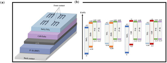
Figure 1.
(a) Schematic of the device layered structure, and (b) energy band diagrams of the materials used in the construction of the solar device.
3. Numerical Simulation and Parameters of Materials
In the framework of this research, SCAPS-1D v3.3.11 software [33,34,35,36], has been employed as a valuable and very effective numerical simulation tool for researching and explaining the physical events that occur within photovoltaic devices [37,38,39]. SCAPS is able to solve Poisson’s equations as well as continuity equations for electrons and holes at every point along the device [40,41]. It achieves this through the use of boundary conditions, and the results from these simulations show strong agreement with experimental data [42]. We aimed to simulate and determine the performance of the inorganic solar cells. We took our analysis a step further by examining how the thicknesses and concentrations of carriers in the absorber and window layers affect the fundamental parameters of the solar cell. To do this, we explored various values of the input variables to determine the optimal values for achieving maximum performance for our solar cell devices.
Table 1, Table 2 and Table 3 provide a list of the properties of the solar device and the material collected from theory, research, and experimentation, defect parameters of the used materials, and Interface defect parameters.

Table 1.
Material parameters used in our simulations [43,44,45,46,47,48,49,50,51].
Table 1.
Material parameters used in our simulations [43,44,45,46,47,48,49,50,51].
| SnO2 | TiO2 | ZnSe | CdS | p-Si | p+-Si | |
|---|---|---|---|---|---|---|
| Thickness (μm) | 0.10 | 0.10 | 0.10 | 0.10 | 0.05 | - |
| Bandgap (eV) | 3.50 | 2.26 | 2.90 | 2.40 | 1.12 | 1.12 |
| Electron affinity (eV) | 4.50 | 4.20 | 4.06 | 4 | 4.05 | 4.05 |
| Relative dielectric permittivity | 9.00 | 9.00 | 10 | 10 | 11.90 | 11.90 |
| CB effective density of states (1/cm3) | 2.2 × 10¹⁷ | 2 × 10¹⁷ | 1.5 × 10¹⁸ | 2.2 × 10¹⁸ | 2.82 × 10¹⁹ | 2.82 × 10¹⁹ |
| VB effective density of states (1/cm3) | 2.2 × 10¹⁶ | 6 × 10¹⁷ | 1.8 × 10¹⁸ | 1.8 × 10¹⁹ | 1.04 × 10¹⁹ | 1.04 × 10¹⁹ |
| Electron thermal velocity (cm/s) | 1 × 10¹⁷ | 1 × 10¹⁷ | 1 × 10¹⁷ | 1 × 10¹⁷ | 1 × 10¹⁷ | 1 × 10¹⁷ |
| Hole thermal velocity (cm/s) | 1 × 10¹⁷ | 1 × 10¹⁷ | 1 × 10¹⁷ | 1 × 10¹⁷ | 1 × 10¹⁷ | 1 × 10¹⁷ |
| Electron mobility (cm2/Vs) | 20 | 100 | 50 | 100 | 1.041 × 10³ | 2.02 × 10² |
| Hole mobility (cm2/Vs) | 10 | 250 | 10 | 25 | 4.12 × 10² | 77 |
| Shallow uniform donor density ND (1/cm3) | 2.42 × 10¹⁹ | 1 × 10¹⁷ | 9 × 10¹⁸ | 1.1 × 10¹⁸ | 1 × 10¹⁶ | 0 |
| Shallow uniform acceptor density NA (1/cm3) | 0 | 0 | 0 | 0 | 1 × 10¹⁶ | 1 × 10¹⁹ |
Table 2.
Defect parameter [42,52].
Table 2.
Defect parameter [42,52].
| TiO2 | SnO2 | ZnSe | CdS | p-Si | |
|---|---|---|---|---|---|
| Defect type | Neutral | Neutral | Neutral | Neutral | Neutral |
| Capture cross section of electrons (cm2) | 1 × 10⁻¹⁵ | 1 × 10⁻¹⁵ | 1 × 10⁻¹⁷ | 1 × 10⁻¹⁷ | 1 × 10⁻¹⁵ |
| Capture cross section of holes (cm2) | 1 × 10⁻¹⁵ | 1 × 10⁻¹⁵ | 1 × 10⁻¹³ | 1 × 10⁻¹³ | 1 × 10⁻¹⁵ |
| Reference for the defect energy level Et | Above the highest Ev | ||||
| Energy with respect to reference (eV) | 0.6 | 0.6 | 0.1 | 0.1 | 0.6 |
| total density (1/cm3) | 1 × 10¹⁴ | 1 × 10¹⁴ | 1 × 10¹⁴ | 1 × 10¹⁴ | 1 × 10¹⁴ |
Table 3.
Interface defect parameter [53,54].
Table 3.
Interface defect parameter [53,54].
| Interface | ||
|---|---|---|
| CdS/SnO2; CdS/TiO2; ZnSe/SnO2; ZnSe/TiO2 | p-Si/CdS; p-Si/ZnSe | |
| Defect type | neutral | neutral |
| Capture cross section of electrons (cm2) | 1 × 10⁻¹⁹ | 1 × 10⁻¹⁹ |
| Capture cross section of holes (cm2) | 1 × 10⁻¹⁹ | 1 × 10⁻¹⁹ |
| Reference for the defect energy level Et | Above the highest Ev | Above the highest Ev |
| Energy with respect to reference (eV) | 0.6 | 0.6 |
| Total density (1/cm3) | 1 × 10¹⁰ | 1 × 10¹⁰ |
4. Results and Discussion
4.1. Influence of Back Surface Field Thickness P+-Si (BSF)
Based on the information provided in Table 1, Table 2 and Table 3, simulations were conducted to analyze how varying the thickness of the surface field layer influences key performance metrics, including open-circuit voltage, short-circuit current density, fill factor, and overall efficiency. These simulations were carried out under standard conditions at 300 K using the AM1.5G solar spectrum.
Figure 2 presents the J_V characteristics of the four heterojunction solar cells studied by varying the back surface field thickness. From the J_V curves, it can be observed that the voltage and current increase as a function of the back surface field thickness. This could be attributed to the augmentation of the back surface field thickness in heterojunction structures, which improves charge carrier collection, reduces recombination, and changes the potential gradients, increasing the voltage and output current of the device. The resulting increase in output current and voltage can make the device more efficient as a photovoltaic cell or in other electronic applications [55,56,57].
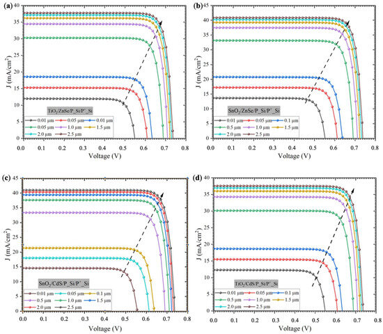
Figure 2.
J-V characteristics of the proposed heterojunctions as a function of the thickness of the back surface field layer of (a) TiO2/ZnSe/P_Si/P+_Si, (b) SnO2/ZnSe/P_Si/P+_Si, (c) SnO2/CdS/P_Si/P+_Si, and (d) TiO2/CdS/P_Si/P+_Si.
In this work, the BSF thickness was varied up to 2.5 µm, which was chosen as an upper limit based on a trade-off between performance gain and practical considerations such as fabrication feasibility and material consumption. Increasing the thickness beyond this value was found to provide marginal improvement in efficiency while potentially introducing higher series resistance and processing complexity. Further increases could also affect the device’s structural integrity or lead to diminishing electrical benefits.
Figure 3 illustrates the quantum efficiency as a function of wavelength for different BSF thicknesses, varying from 0.01 to 2.5 µm. Quantum efficiency indicates the ability of a solar cell to capture charge carriers generated by photons of a certain energy [58]. One notable observation is that as the thickness of the back surface field decreases, the absorption of photons with longer wavelengths decreases. Moreover, at wavelengths greater than 1100 nm, the quantum efficiency drops to zero. This could be caused by the light with longer wavelengths and lower energy cannot be absorbed due to the material’s band gap, which prevents the excitation of charge carriers at these longer wavelengths. In another way, light with too long a wavelength does not have the energy to excite electrons across the band gap, resulting in zero quantum efficiency in this spectral range.
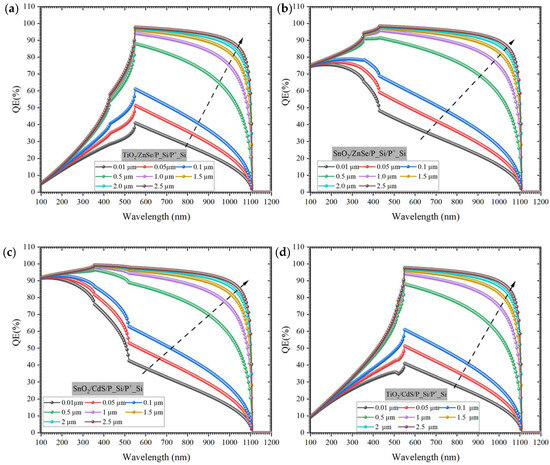
Figure 3.
Quantum efficiency as a function of wavelength for different back surface field thicknesses of (a) TiO2/ZnSe/P_Si/P+_Si, (b) SnO2/ZnSe/P_Si/P+_Si, (c) SnO2/CdS/P_Si/P+_Si, and (d) TiO2/CdS/P_Si/P+_Si.
A significant observation is that for all four solar cells. All solar cell performance parameters improve significantly as the thickness of the BSF layer increases as it is presented in Figure 4. The initial gains in parameters such as short-circuit current density, open-circuit voltage, efficiency, and fill factor were significant as the thickness of the back surface field (BSF) layer increased. However, after a certain point, typically around 2.0 μm, the improvements started to reach a point of optimization. The maximum efficiencies of the cells were approximately 25.2%, 24.8%, 24%, and 23.6% for SnO2/ZnSe/p_Si/p+_Si, SnO2/CdS/p_Si/p+_Si, TiO2/ZnSe/p_Si/p+_Si, and TiO2/CdS/p_Si/p+_Si, respectively. These findings highlight the significance of accuracy in determining the optimal BSF thickness for reaching the best possible solar cell performance. The delicate balance between thickness and performance highlights the need for careful optimization and characterization to ensure the solar cells are operating at their peak efficiency. For the next work, a BSF thickness of 2 μm will be taken as the principle, as this thickness represents the point where the performance of solar cell is typically optimized, based on the previous findings.
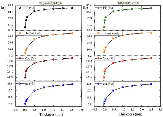
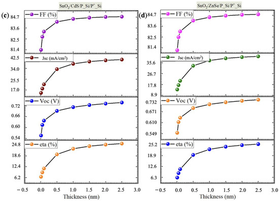
Figure 4.
Influence of the back surface field thickness layer on output parameters of (a) TiO2/ZnSe/P_Si/P+_Si, (b) TiO2/CdS/P_Si/P+_Si, (c) SnO2/CdS/P_Si/P+_Si, and (d) SnO2/ZnSe/P_Si/P+_Si.
4.2. Influence of Doping Concentration of Back Surface Field Thickness (BSF)
The impact of the doping concentration in the back surface field layer was also examined. Figure 5 illustrates the evolution of Voc, Jsc, FF, and the efficiency of photovoltaic cells as a function of the doping density in this layer. At first, it is important to note that all results remained relatively constant until the doping density reached 1014 cm−3, as shown in Figure 5. Thereafter, we observed an increase in Voc with doping density ranging from 1014 cm−3 to 1019 cm−3, reaching 0.74 V for SnO2/ZnSe/p_Si/p+_Si, 0.7 V for SnO2/CdS/p_Si/p+_Si and 0.74 V for TiO2/CdS/p_Si/p+_Si and TiO2/ZnSe/p_Si/p+_Si at 1019 cm−3. The observed behavior of the Jsc is inversely associated with that of Voc, demonstrating a decrease by increasing the doping density of the BSF.
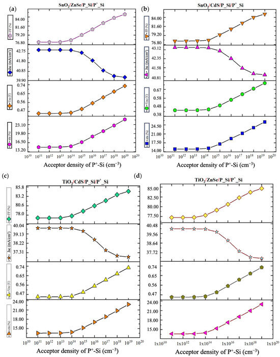
Figure 5.
Influence of the doping density of the back surface field layer on photovoltaic performance of (a) SnO2/ZnSe/P_Si/P+_Si, (b) SnO2/CdS/P_Si/P+_Si, (c) TiO2/CdS/P_Si/P+_Si, and (d) TiO2/ZnSe/P_Si/P+_Si.
The fill factor remained almost constant up to 1016 cm−3 and then significantly increased for all the configurations. At 1019 cm−3 the conversion efficiency reached 24.94% for SnO2/ZnS/p_Si/p+_Si, 25.67% for SnO2/CdS/p_Si/p+_Si, 22.77% for TiO2/CdS/p_Si/p+_Si, and 22.96% for TiO2/ZnSe/p_Si/p+_Si.
Increasing the doping concentration in BSF layer reduces the electrical resistance at the interface between this layer and the p+_Si region. A reduced resistance means less voltage loss across this interface, resulting in a higher open circuit voltage. Increasing the doping concentration in the BSF layer can also increase the Schottky barrier at the interface between the layer and the p+-Si silicon. This helps to reduce carrier recombination at the interface and to create greater separation of charge carriers, which also contributes to an increase in , and also a reduction in contact resistance; better separation of charge carriers generally leads to an enhancement of the fill factor [59,60]. The FF measures how closely the solar cell curve approximates the shape of a rectangle in the current-voltage (I-V) diagram. A higher FF indicates better solar cell performance. In this work, a minimum doping density of 1019 cm−3 in the back surface field layer was chosen for optimum photovoltaic performance.
4.3. Effect of Thickness and Acceptor Density of the Absorber Layers
The relationship between the acceptor density, the thickness of the absorber layer, and the efficiency of a solar cell is complex and can vary depending on the specific materials and cell architecture used. Figure 6 provides information on these parameters in the absorber layer (CdS and ZnSe). The thickness of the absorber layer was evaluated in the interval of 50 nm to 2200 nm, and the dopant concentration (acceptor density) was evaluated in the interval of 1017 cm−3 to 1027 cm−3. The founding displays that decreasing the thickness of the absorber layer increases the efficiency of the solar cell. This can be clarified by the fact that when the absorber layer is thinner, it reduces the distance that charge carriers need to travel to reach the interfaces where they can be collected and contribute to the electrical current, resulting in less recombination of charge carriers and improving the overall efficiency of the solar cell. This phenomenon is particularly observed in solar cells based on thin films, such as those based on technologies like cadmium telluride (CdTe) or copper indium gallium selenide (CIGS). The acceptor density in the absorber layer also shows a central role in the efficiency of the solar cell, as it can affect the electric field distribution and the recombination rate of charge carriers. Optimizing the acceptor density in the absorber layer is an important aspect of solar cell design and can be tailored to the specific materials and cell architecture used to increase the solar cell performance.
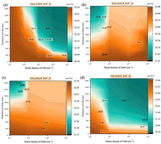
Figure 6.
Contour graphs of heterojunction solar cell performance parameter dependency on defect density and thickness of ETL for (a) SnO2/CdS/P_Si/P+_Si, (b) SnO2/ZnSe/P_Si/P+_Si, (c) TiO2/ZnSe/P_Si/P+_Si, and (d) TiO2/CdS/P_Si/P+_Si.
The acceptor density of the absorber displays a dependency on both the thickness and the type of the absorber. In structures using CdS as absorbers, it is observed that higher efficiencies are reached with thinner layers and lower donor densities. Nevertheless, as the thickness increases, the donor density is required to increase as well to attain higher efficiency. Conversely, in structures employing ZnSe, the highest efficiency is attained with thin layers and low donor densities; increasing these two parameters leads to a decrease in efficiency.
The search results indicate that both CdTe and ZnSe have been explored as absorber materials for multi-junction solar cells. Both materials demonstrated good efficiencies, but since CdS is considered more toxic than ZnSe, ZnSe was chosen as the absorber layer in the subsequent work. The ZnSe absorber layer had a thickness of 80 nm and a donor density of 1018 cm−3.
4.4. Effect of Thickness and Donor Density of the Electron Transport Layers
The performance of solar cells is significantly induced by both the thickness and donor density of the electron transport layer (ETL). Through meticulous adjustment of these parameters, researchers can maintain charge transport efficiency, curtail losses, and strengthen the overall performance and stability of t electronic devices. In purpose of this, the thickness and donor density of the ETL were examined across various configurations. Figure 7 depicts the efficiency of two configurations as functions of the thickness and donor density of different ETLs. The results highlight that higher efficiencies are obtained with smaller thicknesses; conversely, as thickness increases, efficiency diminishes. This trend can be explained by the correlation between the thickness of the ETL and enhanced efficiency in electronic devices. A reduction in thickness lowers carrier transit time, promotes more effective charge extraction, and enhances light absorption in optoelectronic devices such as solar cells. Additionally, thinner ETLs contribute to lower series resistance and optimized interface properties, thereby increasing charge transport efficiency and general device performance.
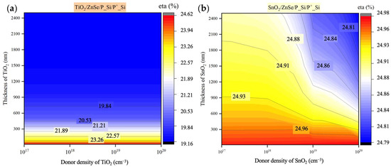
Figure 7.
Contour graphs of heterojunction solar cell performance parameter dependency on defect density and thickness of ETL for: (a) TiO2/ZnSe/P_Si/P+_Si and (b) SnO2/ZnSe/P_Si/P+_Si.
The donor density displays a dependency on both the thickness and the type of electron transport layer (ETL). In structures using SnO2 as the ETL, it is observed that higher efficiencies are reached with thinner layers and lower donor densities. Nevertheless, as the thickness increases, the donor density is required to increase as well to attain higher efficiency. Conversely, in structures employing TiO2, the highest efficiency is attained with thin layers and low donor densities. Increasing these two parameters leads to a reduction in efficiency. SnO2 has been chosen as ETL for the upcoming work, with an optimized thickness of 50 nm and an electron density of 1018 cm−3.
4.5. Influence the Interface Defects
Numerous studies have studied the influence of interface defects on the performance of solar cell devices. Defects at the junction interface can notably impact the optical and the electrical characteristics of the solar cells. Particularly, these defects can escalate the recombination of photo-generated carriers, thereby diminishing the open-circuit voltage, short-circuit current, and overall conversion efficiency. In this study, interface defects between SnO2/ZnSe and ZnSe/P_Si were investigated across a range from 1010 cm−3 to 1018 cm−3, as depicted in Figure 8.
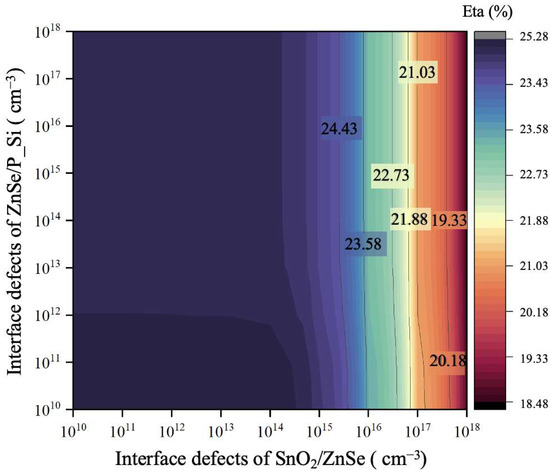
Figure 8.
Influence of interface defects.
The findings demonstrated that interface defects between ZnSe/P_Si exert a lesser influence on the solar cell’s performance, unlike the SnO2/ZnSe interface, where there is a considerable impact. A rise in interface defects between SnO2/ZnSe results in a decline in efficiency. In the subsequent investigation, values of 1014 cm−3 and 1015 cm−3 were considered interface defect densities for ZnSe/P_Si and SnO2/ZnSe, respectively.
4.6. Influence of Back Contact Work Function, Series Resistance (Rs), and Shunt Resistance (Rsh)
The optimization of the performance of solar photovoltaic devices is of crucial importance, and one of the key factors affecting this performance is the presence of series resistors and shunt resistors [61,62]. Understanding the effect of these resistors is important for maximizing the energy efficiency of solar cells. Resistance Rs is a measure of the sum of the resistances present between the cell terminals, including the electrical contacts at the front and rear of the cell. Rsh, on the other hand, is the result of the reverse saturation current generated at the active junction of the cell, generally due to imperfections or manufacturing faults. Both types of resistance have a major impact on solar cell performance.
To assess the influence of Rs and Rsh on critical parameters such as open-circuit voltage, short-circuit current, fill factor, and conversion efficiency, simulations were carried out. Figure 9 displays the variations in , , FF, and efficiency as a function of Rs and Rsh for the selected configuration. For this analysis, Rs was progressively varied from 0 to 6 Ohm·cm2, while keeping Rsh is systematically varied over a range of 0 to 107 Ohm·cm2. These results are essential for understanding how series resistances and shunt resistors affect solar cell functioning, which can guide the design and optimization of photovoltaic devices for maximum efficiency.
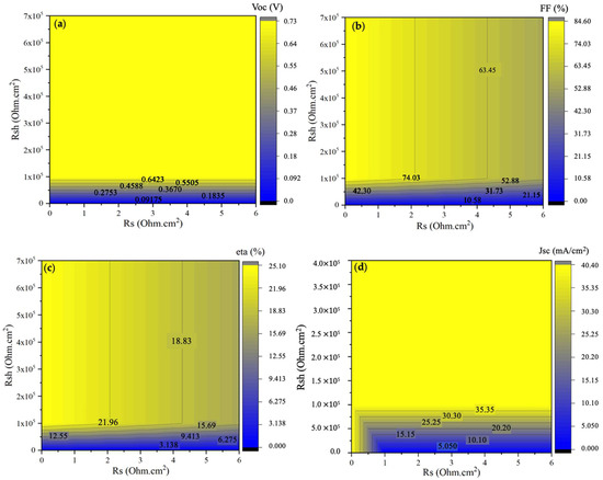
Figure 9.
Influence of series and shunt resistances on photovoltaic performance: (a) Voc, (b) FF, (c) eta, and (d) Jsc.
The increase in Rs had a significant influence on the performance of the solar cells, as shown in Figure 9. and remained relatively stable throughout the Rs variations for Rsh values higher than 105 Ohm·cm2. However, fill factor and efficiency were significantly reduced as Rs increased. The FF decreased significantly from 84.6% when Rs was augmented from 0 to 6 Ohm·cm2 and Rsh from 105 Ohm·cm2 to 7 × 10⁵ Ohm·cm2. Similarly, there was a substantial drop in conversion efficiency, illustrated by the following values: from 25.10% to 16.42 as Rs increased from 0 to 6 Ohm·cm2 for Rsh = 105 Ohm·cm2. This tendency highlights the fact that the increase in series resistance generates a significant power deficit within the solar cell, which inevitably leads to a marked deterioration in the cell’s overall performance. Optimizing and minimizing Rs therefore remain crucial aspects in the design and manufacture of photovoltaic devices to ensure maximum efficiency in converting solar energy into electricity. These observations underline that the conversion efficiency is strongly influenced by the small value of Rsh, while the efficiency reaches a maximum when Rsh increases to a higher value. This study shows conclusively that the photovoltaic performance of the solar cell differs significantly on the two resistances, Rs and Rsh. It is therefore crucial to take these parameters into consideration in the design and manufacture of photovoltaic cells to optimize their overall efficiency.
The photovoltaic parameters of the suggested cell are analyzed as a function of the work function of the back contact, as shown in Figure 10. The purpose of this analysis is to comprehend the practicality of a back contact in the selected device. Indeed, to generate a modest integrated potential at the rear contact, it is imperative to use a material with an appropriate work function at this location.
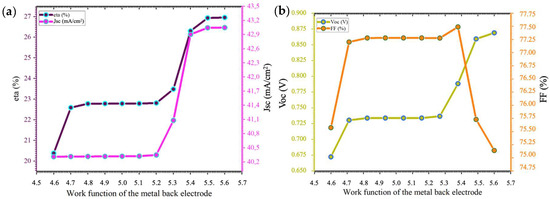
Figure 10.
Influence of back contact work function on photovoltaic performance; (a) Jsc and eta; (b) Voc and FF.
The photovoltaic parameters of the proposed cell are influenced by the variation of the work function of the back contact, which ranges from 4.6 to 5.6 eV, as presented in Figure 10. The observation reveals that all parameters, except , increase as the work function rises from 4.6 to 4.8 eV, then plateau up to 5.2 eV, before reaching their maximum value at 5.6 eV. In contrast, remains constant as the work function is varied until 5.2 eV and then it increases until it reaches its maximum value for the maximum work function of 5.5 eV. This observation indicates that the transport of holes from the absorber to the back contact is limited due to the high barrier formed by materials with a lower work function at the back, leading to reduced solar efficiency [63,64]. It is therefore clear that the work function of the back contact has a significant impact on solar cell performance. In light of current simulation results, it is strongly recommended to use a back contact material with a work function greater than 4.8 eV to ensure sufficient photovoltaic performance. In the coming work, 5.1 eV was selected as the work function, and Rsh = 4 × 10⁵ Ohm·cm2 and Rs = 1.5 Ohm·cm2 as values for the shunt and series resistances.
4.7. Influence of Operating Temperature
In this comprehensive study of the effect of operating temperature on the performance of photovoltaic heterojunctions, significant findings have emerged. Overall, as the temperature increases in the range of 300 to 420 K, all photovoltaic parameters studied, such as open circuit voltage, short circuit current, and conversion efficiency, show a decreasing tendency, as Figure 11 presents. This can be credited to numerous reasons. At higher temperatures, thermal agitation increases, which can promote charge carrier recombination, reducing the global efficiency of photovoltaic conversion. In addition, the intrinsic properties of the materials used in heterojunctions, such as charge carrier mobility, can be negatively affected by temperature, resulting in reduced photovoltaic performance.
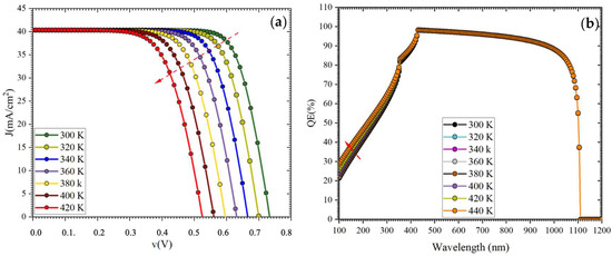
Figure 11.
Influence of temperature of the back surface field layer on (a) J_V and (b) QE.
4.8. Optimized Device Performance
The provided Table 4 and Table 5 outline the optimized parameters for the SnO2/ZnSe/P_Si/p+_Si structure, a critical configuration for enhancing the performance of photovoltaic devices. In this section, gold (Au), characterized by a work function value of 5.1 eV, was considered as a back contact material for simulation. Simultaneously, Figure 12 illustrates the J-V and quantum efficiency (QE) curves. The QE curve visually represents the device’s maximum photon-to-electron conversion efficiency across the electromagnetic spectrum. Notably, the peak QE values occur within the 300 to 1100 nm wavelength range, underscoring the device’s effectiveness in capturing solar energy.
Table 4.
Device parameters for optimized SnO2/ZnSe/P_Si/p+_Si.
Table 5.
Defect and interface defect parameters for optimized SnO2/ZnSe/P_Si/p+_Si.
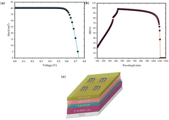
Figure 12.
(a) J-V characteristics, (b) QE curves, and (c) baseline structure solar cell for the final device.
The paramount PSC device parameters achieved through optimization of the electron transport layer (ETL), the absorber layer, series resistance Rs = 1.5 Ohm·cm2, and shunt Rsh = 4 × 10⁵ Ohm·cm2 resistance are as follows: Voc = 0.734 V, Jsc = 40.33 mA/cm2, FF = 77.05%, and = 22.82%. These combined parameters signify the excellence of this photovoltaic device, demonstrating high efficiency and optimal performance in the conversion of sunlight into electricity.
5. Conclusions
In this work, a comprehensive analysis of the performance of various solar cell configurations, including SnO2/ZnSe/p_Si/p+_Si, SnO2/CdS/p_Si/p+_Si, TiO2/ZnSe/p_Si/p+_Si, and TiO2/CdS/p_Si/p+_Si were conducted. We highlighted the importance of key factors such as the back surface field thickness, doping concentration of BSF, operating temperature, back contact work function, defect density, and series and shunt resistance on the performance parameters of open-circuit voltage, short-circuit current density, fill factor and quantum efficiency.
Our results conclusively indicate that each of these parameters shows an essential role in determining the overall efficiency of solar cells, and their optimization is crucial to maximize the conversion of solar energy into electricity. Among the configurations examined, two of them stood out: SnO2/ZnSe/p_Si/p+_Si and SnO2/CdS/p_Si/p+_Si. While both configurations demonstrated promising performance, the environmental impact of CdS, a toxic material, merits attention. Substituting CdS with ZnSe in the SnO2/ZnSe/p_Si/p+_Si configuration resulted in significant performance improvements and a more environmentally responsible approach. Our study revealed that this substitution is not only environmentally responsible but also led to a significant improvement in performance. Specifically, the SnO2/ZnSe/p_Si/p+_Si configuration, with a back surface field thickness of and a doping concentration of 1019 cm−3, emerged as the most favorable configuration. It exhibited a marked increase in open-circuit voltage, short-circuit current density, and fill factor. Energy conversion efficiency was substantially improved compared to other configurations studied. Furthermore, the quantum efficiency was also favorable for this configuration, confirming its potential for advanced photovoltaic applications.
Author Contributions
Conceptualization, A.Z. and A.L.; methodology, A.L., A.Z. and M.T.; software, A.L., A.A., P.P.; validation, A.A.B., P.P., A.Z., A.H. and M.T.; formal analysis, A.L., K.W., M.T.; investigation, A.L., M.T., P.P.; data curation, A.L., K.W. and P.P.; writing—original draft preparation, A.L.; writing—review and editing, A.Z., A.A.B., P.P. and M.T.; visualization, A.L., P.P. and A.Z.; supervision, A.Z., A.A.B. and A.H.; funding acquisition, A.L. All authors have read and agreed to the published version of the manuscript.
Funding
The research was carried out as part of the IDUB project—emerging research fields: “Material Science and Technology”.
Institutional Review Board Statement
Not applicable.
Informed Consent Statement
Not applicable.
Data Availability Statement
Data is contained within the article.
Acknowledgments
All authors gratefully acknowledge the SCAPS simulation software provided by Marc Burgelman, ELSI, University of Gent, Belgium. H.D.
Conflicts of Interest
The authors declare no conflict of interest.
References
- Owusu, P.A.; Asumadu-Sarkodie, S. A review of renewable energy sources, sustainability issues and climate change mitigation. Cogent Eng. 2016, 3, 1167990. [Google Scholar] [CrossRef]
- Mele, M.; Gurrieri, A.R.; Morelli, G.; Magazzino, C. Nature and climate change effects on economic growth: An LSTM experiment on renewable energy resources. Environ. Sci. Pollut. Res. 2021, 28, 41127–41134. [Google Scholar] [CrossRef] [PubMed]
- Hosseinnezhad, M.; Gharanjig, K.; Yazdi, M.K.; Zarrintaj, P.; Moradian, S.; Saeb, M.R.; Stadler, F.J. Dye-sensitized solar cells based on natural photosensitizers: A green view from Iran. J. Alloys Compd. 2020, 828, 154329. [Google Scholar] [CrossRef]
- Li, G.; Li, M.; Taylor, R.; Hao, Y.; Besagni, G.; Markides, C.N. Solar energy utilisation: Current status and roll-out potential. Appl. Therm. Eng. 2022, 209, 118285. [Google Scholar] [CrossRef]
- Laouid, A.; Alaoui Belghiti, A.; Wisniewski, K.; Hajjaji, A.; Sahraoui, B.; Zawadzka, A. Generation of red light with intense photoluminescence assisted by Forster resonance energy transfer from Znq2 and DCM thin films. Environ. Sci. Pollut. Res. 2022, 30, 81647–81666, 1–20. [Google Scholar] [CrossRef]
- Abbood, A.M.; Abed, Q.A. Using the nano-composite coating technology to improve PV solar cell performance: A review. AIP Conf. Proc. 2023, 2776, 090001. [Google Scholar] [CrossRef]
- Laouid, A.; Alaoui Belghiti, A.; Wisniewski, K.; Strzelecki, J.; Karakas, A.; Gozutok, A.; El kouari, Y.; Bouich, A.; Tlemçani, M.; Plociennik, P.; et al. Optical and morphological properties of DCM thin films co-doped of Znq2 by PVD: Theoretical and experimental investigations. Vacuum 2024, 222, 112997. [Google Scholar] [CrossRef]
- Mamta; Kumar, R.; Kumari, R.; Maurya, K.K.; Singh, V.N. Sb2(S, Se)3-based photovoltaic cell with MoS2 as a hole transport layer: A numerical investigation. Mater. Today Sustain. 2022, 20, 100218. [Google Scholar] [CrossRef]
- Laouid, A.; Alaoui Belghiti, A.; Wisniewski, K.; Hajjaji, A.; Zawadzka, A. Structural and optical properties of DCM thin films prepared by PVD. Mater. Today Proc. 2022, 66, 63–67. [Google Scholar] [CrossRef]
- Laouid, A.; Alaoui Belghiti, A.; Wisniewski, K.; Boumhamdi, M.; Strzelecki, J.; Plociennik, P.; Hajjaji, A.; Zawadzka, A. A study of morphological, optical, and photoluminescence properties of ZnS thin films doped Mn and ca. Mater. Chem. Phys. 2024, 318, 129270. [Google Scholar] [CrossRef]
- Nikpay, M.A.; Mortazavi, S.Z.; Aghaei, M.; Elahi, S.M.; Reyhani, A. Prospect of single and coupled heterojunction solar cells based on n-MoS2 and n-WS2. Mater. Sci. Eng. B 2021, 274, 115493. [Google Scholar] [CrossRef]
- Zyoud, S.H.; Zyoud, A.H.; Ahmed, N.M.; Abdelkader, A.F.I. Numerical Modelling Analysis for Carrier Concentration Level Optimization of CdTe Heterojunction Thin Film–Based Solar Cell with Different Non–Toxic Metal Chalcogenide Buffer Layers Replacements: Using SCAPS–1D Software. Crystals 2021, 11, 1454. [Google Scholar] [CrossRef]
- Bilal, B.; Najeeb-ud-Din, H. Towards low cost, industrially compatible silicon heterojunction solar cells using hybrid carrier selective passivating contacts. Opt. Mater. 2022, 124, 111957. [Google Scholar] [CrossRef]
- Kiruthiga, G.; Rajni, K.S.; Geethanjali, N.; Raguram, T.; Nandhakumar, E.; Senthilkumar, N. SnO2: Investigation of optical, structural, and electrical properties of transparent conductive oxide thin films prepared by nebulized spray pyrolysis for photovoltaic applications. Inorg. Chem. Commun. 2022, 145, 109968. [Google Scholar] [CrossRef]
- Yadav, S.; Yadav, K.; Dhar, R.; Mohan, D. Synthesis and characterization of thermally evaporated Er-doped SnO2 thin films for photonic applications. Micro Nanostructures 2023, 174, 207493. [Google Scholar] [CrossRef]
- Brunet, E.; Maier, T.; Mutinati, G.C.; Steinhauer, S.; Köck, A.; Gspan, C.; Grogger, W. Comparison of the gas sensing performance of SnO2 thin film and SnO2 nanowire sensors. Sens. Actuators B Chem. 2012, 165, 110–118. [Google Scholar] [CrossRef]
- Su, L.; Zuo, Y.; Xie, J. Scalable manufacture of vertical p-GaN/n-SnO2 heterostructure for self-powered ultraviolet photodetector, solar cell and dual-color light emitting diode. InfoMat 2021, 3, 598–610. [Google Scholar] [CrossRef]
- Jaishree, N.; Hashmi, A.; Katre, Y.R.; Singh, R.S.; Singh, J.; Srivastava, A.; Singh, A.K. The influence of different complexing agents on the properties of tin dioxide (SnO2) deposited thin films through chemical bath approach. Phys. B Condens. Matter 2023, 650, 414520. [Google Scholar] [CrossRef]
- Soumya, S.S.; Xavier, T.S. Effect of cobalt doping on the microstructural, optical and electrical properties of SnO2 thin films by sol-gel spin coating technique. Phys. B Condens. Matter 2022, 624, 413432. [Google Scholar] [CrossRef]
- Gupta, S.P.; Sanap, P.P.; Dilwale, G.V.; Bulakhe, R.N.; Jagadale, A.D.; Deore, M.K.; Bhalerao, A.B.; Lokhande, C.D. Nanostructured Zinc Selenide (ZnSe) Thin Films Deposited by Various Modes of Electrodeposition for Photovoltaic Application. ES Energy Environ. 2023, 20, 910. [Google Scholar] [CrossRef]
- Ikhioya, I.L.; Ugwuoke, C.O.; Okoli, D.N.; Ekpunobi, A.J.; Maaza, M.; Ezema, F.I. Effect of cobalt on the photovoltaic properties of zinc selenide thin film deposited on fluorine-doped tin oxide (FTO) via electrochemical deposition technique. Curr. Res. Green Sustain. Chem. 2022, 5, 100328. [Google Scholar] [CrossRef]
- Ikhioya, I.L.; Nkele, A.C.; Okoli, D.N. Effects of temperature and ph variations on electrochemically-deposited zirconium-doped zinc selenide thin films. Optik 2022, 260, 169055. [Google Scholar] [CrossRef]
- Ganesha Krishna, V.S.; Mahesha, M.G. Analysis of surface properties of Mg doped ZnS and ZnSe thin films through x-ray photoelectron spectroscopy. J. Electron Spectrosc. Relat. Phenom. 2023, 266, 147341. [Google Scholar] [CrossRef]
- Najm, A.S.; Naeem, H.S.; Alabboodi, K.O.; Hasbullah, S.A.; Hasan, H.A.; Holi, A.M.; AL-Zahrani, A.A.; Sopian, K.; Bais, B.; Majdi, H.S.; et al. New systematic study approach of green synthesis CdS thin film via Salvia dye. Sci. Rep. 2022, 12, 12521. [Google Scholar] [CrossRef]
- El-Shaer, A.; Ezzat, S.; Habib, M.A.; Alduaij, O.K.; Meaz, T.M.; El-Attar, S.A. Influence of Deposition Time on Structural, Morphological, and Optical Properties of CdS Thin Films Grown by Low-Cost Chemical Bath Deposition. Crystals 2023, 13, 788. [Google Scholar] [CrossRef]
- Ismail, W.; Ibrahim, G.; Habib, M.A.; Alduaij, O.K.; Abdelfatah, M.; El-Shaer, A. Advancement of Physical and Photoelectrochemical Properties of Nanostructured CdS Thin Films toward Optoelectronic Applications. Nanomaterials 2023, 13, 1764. [Google Scholar] [CrossRef]
- Ge, S.; Sang, D.; Zou, L.; Yao, Y.; Zhou, C.; Fu, H.; Xi, H.; Fan, J.; Meng, L.; Wang, C. A Review on the Progress of Optoelectronic Devices Based on TiO2 Thin Films and Nanomaterials. Nanomaterials 2023, 13, 1141. [Google Scholar] [CrossRef]
- Yousefi, F.; Mousavi, S.B.; Heris, S.Z.; Naghash-Hamed, S. UV-shielding properties of a cost-effective hybrid PMMA-based thin film coatings using TiO2 and ZnO nanoparticles: A comprehensive evaluation. Sci. Rep. 2023, 13, 7116. [Google Scholar] [CrossRef]
- Althamthami, M.; Guettaf Temam, E.; Temam, H.B.; Saad, R.; Hasan, G.G. Improved photocatalytic activity under the sunlight of high transparent hydrophilic Bi-doped TiO2 thin-films. J. Photochem. Photobiol. A Chem. 2023, 443, 114818. [Google Scholar] [CrossRef]
- Kanmaz, İ. Simulation of CdS/p-Si/p+-Si and ZnO/CdS/p-Si/p+-Si heterojunction solar cells. Results Opt. 2023, 10, 100353. [Google Scholar] [CrossRef]
- Titova, A.M.; Shengurov, V.G.; Filatov, D.O.; Denisov, S.A.; Chalkov, V.Y.u.; Ved’, M.V.; Zaitzev, A.V.; Sushkov, A.A.; Alyabina, N.A. Epitaxial n+-Ge/p+-Si(001) heterostructures with ultra sharp doping profiles for light emitting diode applications. Mater. Sci. Eng. B 2023, 289, 116219. [Google Scholar] [CrossRef]
- Lee, H.J.; Kim, D.; Choi, W.S.; Kim, C.; Choi, S.-J.; Bae, J.-H.; Kim, D.M.; Kim, S.; Kim, D.H. Effect of oxygen flow rate on long-term and short-term Schottky barrier modulations in Pd/IGZO/SiO2/p+-Si memristors. Mater. Sci. Semicond. Process. 2023, 153, 107183. [Google Scholar] [CrossRef]
- Al-Hattab, M.; Moudou, L.; Khenfouch, M.; Bajjou, O.; Chrafih, Y.; Rahmani, K. Numerical simulation of a new heterostructure CIGS/GaSe solar cell system using SCAPS-1D software. Sol. Energy 2021, 227, 13–22. [Google Scholar] [CrossRef]
- Kumari, N.; Ingole, S. Enhancement of CZTS photovoltaic device performance with silicon at back-contact: A study using SCAPS-1D. Sol. Energy 2022, 236, 301–307. [Google Scholar] [CrossRef]
- Yadav, R.K.; Pawar, P.S.; Nandi, R.; Neerugatti, K.E.; Kim, Y.T.; Cho, J.Y.; Heo, J. A qualitative study of SnSe thin film solar cells using SCAPS 1D and comparison with experimental results: A pathway towards 22.69% efficiency. Sol. Energy Mater. Sol. Cells 2022, 244, 111835. [Google Scholar] [CrossRef]
- Salem, M.S.; Shaker, A.; Almurayziq, T.S.; Alshammari, M.T. Prospective efficiency boosting of full-inorganic single-junction Sb2(S, Se)3 solar cell. Sol. Energy Mater. Sol. Cells 2022, 248, 112001. [Google Scholar] [CrossRef]
- Ouédraogo, S.; Zougmoré, F.; Ndjaka, J.M. Numerical Analysis of Copper-Indium-Gallium-Diselenide-Based Solar Cells by SCAPS-1D. Int. J. Photoenergy 2013, 2013, 421076. [Google Scholar] [CrossRef]
- Djinkwi Wanda, M.; Ouédraogo, S.; Tchoffo, F.; Zougmoré, F.; Ndjaka, J.M.B. Numerical Investigations and Analysis of Cu2ZnSnS4 Based Solar Cells by SCAPS-1D. Int. J. Photoenergy 2016, 2016, 2152018. [Google Scholar] [CrossRef]
- Burgelman, M.; Nollet, P.; Degrave, S. Modelling polycrystalline semiconductor solar cells. Thin Solid Films 2000, 361–362, 527–532. [Google Scholar] [CrossRef]
- Abdelfatah, M.; El Sayed, A.M.; Ismail, W.; Ulrich, S.; Sittinger, V.; El-Shaer, A. SCAPS simulation of novel inorganic ZrS2/CuO heterojunction solar cells. Sci. Rep. 2023, 13, 4553. [Google Scholar] [CrossRef]
- Shankar, G.; Kumar, P.; Pradhan, B. All-perovskite two-terminal tandem solar cell with 32.3% efficiency by numerical simulation. Mater. Today Sustain. 2022, 20, 100241. [Google Scholar] [CrossRef]
- Ait Abdelkadir, A.; Sahal, M. Theoretical development of the CZTS thin-film solar cell by SCAPS-1D software based on experimental work. Mater. Sci. Eng. B 2023, 296, 116710. [Google Scholar] [CrossRef]
- Ritu; Gagandeep; Kumar, R.; Chand, F. Optimization of ITO/SnO2/FASnI3/PCBM/Ag based perovskite solar cell. Mater. Today Proc. 2023. [Google Scholar] [CrossRef]
- Johrin, N.; Chee, F.P.; Nasir, S.; Moh, P.Y. Numerical study and optimization of GO/ZnO based perovskite solar cell using SCAPS. AIMS Energy 2023, 11, 683–693. [Google Scholar] [CrossRef]
- Zyoud, S.; Zyoud, A. Simulation and Numerical Investigation of the Effect of Temperature and Defect on ZnTe/ZnSe/ZnO Thin-Film Photovoltaic Solar Cell Performance Efficiency. Int. J. Eng. Appl. 2023, 11, 1–10. [Google Scholar] [CrossRef]
- El Ouarie, N.; El Hamdaoui, J.; Sahoo, G.S.; Rodriguez-Osorio, K.G.; Courel, M.; Zazoui, M.; Pérez, L.M.; Laroze, D.; Feddi, E. Modeling of highly efficient CNGS based kesterite solar cell: A DFT study along with SCAPS-1D analysis. Sol. Energy 2023, 263, 111929. [Google Scholar] [CrossRef]
- Kannan, P.K.; Anandkumar, M. A theoretical investigation to boost the efficiency of CZTS solar cells using SCAPS-1D. Optik 2023, 288, 171214. [Google Scholar] [CrossRef]
- Shukla, V.; Panda, G. The performance study of CdTe/CdS/SnO2 solar cell. Mater. Today Proc. 2020, 26, 487–491. [Google Scholar] [CrossRef]
- Faremi, A.A.; Olubosede, O.; Salau, A.O.; Adigbo, S.O.; Olubambi, P.A.; Lawan, E. Variability of temperature on the electrical properties of heterostructured CIS/Cds through SCAPS simulation for photovoltaic applications. Mater. Renew. Sustain. Energy 2023, 12, 235–246. [Google Scholar] [CrossRef]
- Biswas, S.K.; Ahmed, M.M.; Orthe, M.F.; Sumon, M.S.; Sarker, K. Numerical Investigation of High Efficiency Cu2SnSe3 Thin Film Solar Cell with a Suitable ZnSe Buffer Layer Using SCAPS 1D Software. Eur. J. Electr. Eng. Comput. Sci. 2023, 7, 63–70. [Google Scholar] [CrossRef]
- Mamta; Singh, Y.; Maurya, K.K.; Singh, V.N. n-Si/p-Sb2Se3 structure based simple solar cell device. Mater. Today Sustain. 2022, 18, 100148. [Google Scholar] [CrossRef]
- Souri, S.; Marandi, M. Numerical modelling of the effect of the Ag: ZnSe BSF layer on the high performance of ZnSe/CdTe thin film solar cells by SCAPS-1D software. Opt. Quantum Electron. 2023, 55, 397. [Google Scholar] [CrossRef]
- Bliya, A.; Lachhab, S.E.; Al Ibrahmi, E. Improving the semiconductor performance of SnO2/CdS/CuBi2O4 by optimizing the optical properties of the CuBi2O4 absorbent layer. Micro Nanostructures 2023, 183, 207667. [Google Scholar] [CrossRef]
- Chauhan, S.; Singh, R. Analysis of absorber layer for wide-bandgap double perovskite solar cell using SCAPS-1D. Mater. Today Proc. 2023. [Google Scholar] [CrossRef]
- Ahmed, S.R.A.; Sunny, A.; Rahman, S. Performance enhancement of Sb2Se3 solar cell using a back surface field layer: A numerical simulation approach. Sol. Energy Mater. Sol. Cells 2021, 221, 110919. [Google Scholar] [CrossRef]
- Wang, J.C.; Ren, X.C.; Shi, S.Q.; Leung, C.W.; Chan, P.K.L. Charge accumulation induced S-shape J–V curves in bilayer heterojunction organic solar cells. Org. Electron. 2011, 12, 880–885. [Google Scholar] [CrossRef]
- Schulte, K.L.; Simon, J.; Steiner, M.A.; Ptak, A.J. Modeling and design of III–V heterojunction solar cells for enhanced performance. Cell Rep. Phys. Sci. 2023, 4, 101541. [Google Scholar] [CrossRef]
- Barman, B.; Kalita, P.K. Influence of back surface field layer on enhancing the efficiency of CIGS solar cell. Sol. Energy 2021, 216, 329–337. [Google Scholar] [CrossRef]
- Benzetta, A.E.H.; Abderrezek, M.; Djeghlal, M.E. Contribution to improve the performances of Cu2ZnSnS4 thin-film solar cell via a back surface field layer. Optik 2019, 181, 220–230. [Google Scholar] [CrossRef]
- Karade, V.C.; Jang, J.S.; Kumbhar, D.; Rao, M.; Pawar, P.S.; Kim, S.; Gour, K.S.; Park, J.; Heo, J.; Dongale, T.D.; et al. Combating open circuit voltage loss in Sb2Se3 solar cell with an application of SnS as a back surface field layer. Sol. Energy 2022, 233, 435–445. [Google Scholar] [CrossRef]
- Bal, S.S.; Basak, A.; Singh, U.P. Numerical modeling and performance analysis of Sb-based tandem solar cell structure using SCAPS—1D. Opt. Mater. 2022, 127, 112282. [Google Scholar] [CrossRef]
- Khan, R.; Ahmed, S.F.; Khalid, M.; Joshi, B. Investigating Effect of CdS Buffer Layer on the Performance of Cu2ZnSnS4 Based Solar Cells Using SCAPS-1D. Trans. Electr. Electron. Mater. 2021, 22, 177–184. [Google Scholar] [CrossRef]
- Ratcliff, E.L.; Garcia, A.; Paniagua, S.A.; Cowan, S.R.; Giordano, A.J.; Ginley, D.S.; Marder, S.R.; Berry, J.J.; Olson, D.C. Investigating the Influence of Interfacial Contact Properties on Open Circuit Voltages in Organic Photovoltaic Performance: Work Function Versus Selectivity. Adv. Energy Mater. 2013, 3, 647–656. [Google Scholar] [CrossRef]
- Nowsherwan, G.A.; Iqbal, M.A.; Rehman, S.U.; Zaib, A.; Sadiq, M.I.; Dogar, M.A.; Azhar, M.; Maidin, S.S.; Hussain, S.S.; Morsy, K.; et al. Numerical optimization and performance evaluation of ZnPC:PC70BM based dye-sensitized solar cell. Sci. Rep. 2023, 13, 10431. [Google Scholar] [CrossRef] [PubMed]
Disclaimer/Publisher’s Note: The statements, opinions and data contained in all publications are solely those of the individual author(s) and contributor(s) and not of MDPI and/or the editor(s). MDPI and/or the editor(s) disclaim responsibility for any injury to people or property resulting from any ideas, methods, instructions or products referred to in the content. |
© 2025 by the authors. Licensee MDPI, Basel, Switzerland. This article is an open access article distributed under the terms and conditions of the Creative Commons Attribution (CC BY) license (https://creativecommons.org/licenses/by/4.0/).