Article

Optical Property and Stability Study of CH3(CH2)3NH3)2(CH3NH3)3Pb4I13 Ruddlesden Popper 2D Perovskites for Photoabsorbers and Solar Cells and Comparison with 3D MAPbI3

by
Kakaraparthi Kranthiraja
1,†,
Sujan Aryal
1,†,
Mahdi Temsal
1,†,
Mohin Sharma
1,† and
Anupama B. Kaul
1,2,*
1
Department of Electrical Engineering, PACCAR Technology Institute, University of North Texas, Denton, TX 76203, USA
2
Department of Materials Science and Engineering, University of North Texas, Denton, TX 76203, USA
*
Author to whom correspondence should be addressed.
These authors contributed equally to this work.
Solar 2022, 2(4), 385-400; https://doi.org/10.3390/solar2040023
Submission received: 14 June 2022 / Revised: 17 August 2022 / Accepted: 29 August 2022 / Published: 20 September 2022

Abstract

:
Three dimensional (3D) perovskite solar cells (PSCs) are a promising candidate for third-generation photovoltaics (PV) technology, which aims to produce efficient photon conversion devices to electricity using low-cost fabrication processes. Hybrid organic-inorganic perovskites for-lmed using low-cost solution processing are explored here, which have experienced a stupendous rise in power conversion efficiency (PCE) over the past decade and serve as a prime candidate for third-generation PV systems. While significant progress has been made, the inherent hygroscopic nature and stability issue of the 3D perovskites (3DPs) are an impediment to its commercialization. In this work, we have studied two-dimensional (2D) organometallic halide (CH3(CH2)3NH3)2(CH3NH3)n−1PbnI3n+1) layered perovskites in the Ruddlesden Popper structure, represented as BA2MA3Pb4I13 for the n = 4 formulation, for both photoabsorbers in a two-terminal architecture and solar cells, given that these material are considered to be inherently more stable. In the two-terminal photo absorber devices, the photocurrent and responsivity were measured as a function of incoming laser wavelength, where the location of the peak current was correlated to the emission spectrum arising from the 2DP film using photoluminescence (PL) spectroscopy. The 2D (BA)2(MA)3Pb4I13 films were then integrated into an n-i-p solar cell architecture, and PV device figures of merit tabulated, while our 3D MAPbI3 served as the reference absorber material. A comparative study of the 3DP and 2DP film stability was also conducted, where freshly synthesized films were inspected on FTO substrates and compared to those exposed to elevated humidity levels, and material stability was gauged using various material characterization probes, such as PL and UV-Vis optical absorption spectroscopy, scanning electron microscopy and X-ray diffraction. While the PCE of the 3D-PSCs was higher than the 2D-PSCs, our results confirm the enhanced environmental stability of the 2DP absorber films compared to the 3DP absorbers, suggesting their promise to address the stability issue broadly encountered in 3D PSCs toward third-generation PV technology.

Graphical Abstract

1. Introduction

Clean alternative energy sources are critical to addressing one of humanity’s grand challenges, given our dependence on fossil fuels which produce harmful CO2 emissions that exacerbates global warming. With the worldwide demand for energy expected to triple by the end of the century, and coupled with the limited planetary fossil fuel reserves, the need to develop high-efficiency, low-cost energy harvesting devices as a clean energy source is imperative and urgent. Renewable energy sources based on energy harvesting photovoltaic (PV) solar cell devices are a prime candidate for helping address the rising energy demand, where efficient light absorbing material systems play a pivotal role. These material systems include amorphous silicon (Si), copper indium gallium selenide (CIGS), cadmium telluride (CdTe), organic materials for organic photovoltaics (OPV), in addition to dye sensitized solar cells (DSSCs). More recently, perovskite solar cells (PSCs) have come into the picture as well, as an exciting candidate for third-generation PV technology, which aims to deliver efficient photon conversion devices to electricity at low-cost [1,2,3]. The geometrical stability and allowed range of tolerance offer a broad compositional space for chemical engineering of new perovskites by systematic substitution of cationic and anionic constituents and to obtain mixed-cation or mixed-anion perovskites through isovalent substitution in the parent 3DP compound [4].
Organic–inorganic hybrid perovskites are described by the general formula AMX3, where A is usually a large organic cation such as RH3N+. Here R is an alkyl group ranging from methylammonium (MA: CH3NH3+), ethylammonium (EA: CH3CH2NH3+), butylammonium (BA: CH3(CH2)3NH3+). Additionally, M is a divalent metal such as Pb2+ or Sn2+, while X is a halogen anion such as Cl, I, Br. Perovskites have remarkable properties which includes wide spectral absorption from the ultraviolet (UV) to the near-infrared (NIR) region, high absorption coefficient and light yield (~50,000 photons/MeV), long carrier lifetime (~102~103 ns) and carrier diffusion length (up to ~1 μm), low-exciton binding energy (<10 meV), high carrier mobility and low charge carrier recombination rates [5,6,7,8,9,10,11,12]. From these remarkable properties, it is no surprise PSCs are considered promising for third-generation PV technology, with a key feature being their low-cost solution processibility, which has triggered extensive research to further unveil their outstanding optoelectronic properties [13]. The boost in power conversion efficiency (PCE) of PSCs has led to a certified value of 25.7% after intensive research over the past decade [14]. Beyond the PV community, these properties have also led to their use in other optoelectronic applications, such as light-emitting diodes, photodetectors, lasers, image sensors, and displays [15,16,17,18,19].
The most commonly explored three-dimensional perovskite (3DP) is MAPbI3 [20,21,22,23,24], and despite the rapid progress that has been witnessed recently with this material, one of the bottlenecks to delaying commercialization is its long-term stability [25,26,27,28,29]. A primary reason for the poor stability of PSCs arises from the intrinsic nature of the 3DP itself, such as FAPbI3 besides of course MAPbI3, given the rapid degradation and breakdown of the absorber into PbI2 in the presence of moisture, UV radiation, temperature, and oxygen [30,31]. The hygroscopic behavior of 3DPs often causes a hydrated phase of the perovskite to form via weak hydrogen bonds with perovskite cations that further leads to decomposition of the crystals [32,33]. Dopants associated with the hole transport layers (HTLs), such as Spiro-OMeTAD/PTAA are also responsible for the indirect degradation of the absorber to some extent, while the severe hygroscopic nature of other HTLs such as PEDOT:PSS [34] is well known to also destabilize the PSC [35,36]. Alongside these extrinsic parameters, intrinsic factors based on defect-mediated ion migration within the perovskite absorber also leads to poor long-term performance of PSCs. Numerous approaches have been used to ameliorate the stability of the 3DP themselves, as well as the contact layers [37,38,39]. Variants in the cations (e.g., the use of Cs and FA for the A-site cation for triple cation absorbers), as well as mixed halides (e.g., Br and I for the X-site) appear to enhance stability to some extent [36,40,41]. Additionally, the restricted composition available in the AMX3 perovskite structure is a significant impediment to further development, since there are just three A-site cations able to sustain the 3D corner-sharing inorganic framework, resulting in only metastable compounds in certain circumstances [42,43].
Reducing dimensionality of the 3DP to the two-dimensional perovskites (2DPs) [44,45], including in the 2D Ruddlesden-Popper (2DRP) phase, is gaining momentum [46], though PCEs of 2D PSCs are typically lower. The 2DPs provide significant relief from the restricted compositional variety present within the 3DP [47,48]. Single (or many) inorganic sheets are sandwiched between organic spacers which are held together by Coulombic forces. The standard formula for 2DPs can be represented as (A′)m(A)n−1BnX3n+1, where A’ is a bulky organic cation (such as an aliphatic or aromatic alkylammonium) that functions as a spacer between the inorganic sheets, and n is the number of inorganic layers held together. The layered structure reduces the Goldschmidt tolerance factor’s limitations on cation size and unlike 3DPs, allows bulky A’ cations to be accommodated via van der Waals interactions between the inorganic sheets.
In this study, we have examined the optoelectronic properties of 2DRPs absorber, specifically ((CH3(CH2)3NH3)2(CH3NH3)3Pb4I13), and its integration into a solar cell architecture is also discussed, where a comparative analysis is conducted with 3DP absorbers, specifically MAPbI3. In the first part of this work, we discuss the synthesis approach used for the ((CH3(CH2)3NH3)2(CH3NH3)3Pb4I13) 2DP, which may be considered to be part of the broader 2D layered materials family that are emerging as promising candidates for optoelectronics [49,50,51]. The 2DP was synthesized using previously reported approaches [52,53,54,55], and material characterization studies on the environmental stability of the absorber were conducted using techniques such as steady state photoluminescence (PL) spectroscopy, scanning electron microscopy (SEM), and X-ray diffraction (XRD). The optoelectronic properties of the 2DP absorber were deduced from photoabsorber measurements through the determination of the responsivity which was correlated to the PL emission characteristics of the intrinsic absorber. Through our work it is clear the 2DPs offer promising photoabsorption characteristics while also being more environmentally stable under ambient conditions compared to MAPbI3, to address stability concerns intrinsic to these 3DP photoabsorbers.

2. Results and Discussion

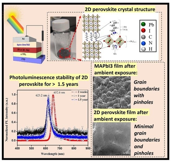
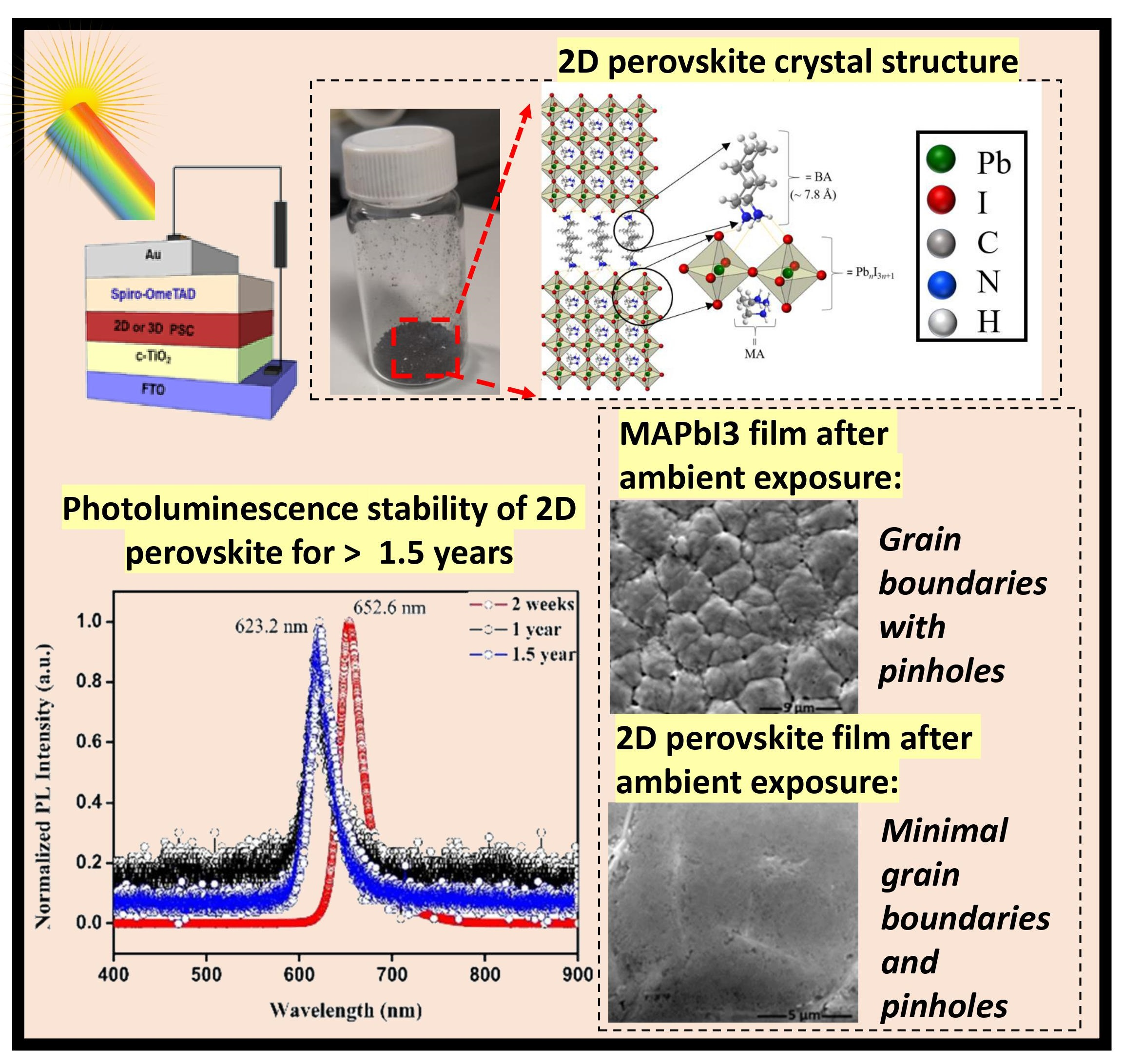
2.1. Synthesis and Characterization of 2DRP

In the 2DRP phase, the inorganic layer of the octahedra comprise of Pb atoms that share the halide ions with its neighboring metal atom in a 2D plane. The organic groups self-assemble through van der Waals interactions to form butylammonium (BA) and methylammonium (MA) layers where the ammonium head of the organic groups, namely CH3(CH2)3NH3 and CH3NH3, binds to Pb4I13 molecules through the van der Waals interaction. We synthesized our 2DP (BA)2(MA)3Pb4I13 formulation using the process illustrated in the Figure 1a. The PbO powder (2232 mg) was dissolved in a mixture of 57% w/w aqueous HI solution (10.0 mL) and 50% aqueous H3PO2 (1.7 mL) with heating at 130 °C and subsequent boiling under constant stirring for about 25 min. Into this solution, CH3NH3Cl (507 mg) was subsequently added, which initially caused the precipitation of a black powder that quickly re-dissolved under stirring to yield a clear bright-yellow solution. Additionally, n-CH3(CH2)3NH3I (248 μL) and HI acid (5 mL) were mixed separately in a glass vial and this mixture was then added dropwise to the previous solution under vigorous stirring for 10 min. The solution was then left to cool down to room temperature which resulted in the formation of dark black, rectangular-shaped platelets. The crystals were isolated by suction filtration and thoroughly dried under reduced pressure [52,56,57], as shown by the powder collected in a vial in Figure 1b-left. The crystal structure for the n = 4 formulation is depicted in Figure 1b-right, where the metal-halide octahedral sheets of the AMX3 complex are connected by the intercalated BA bilayer with an effective gap of ~15.6Å. The repeat unit of the ordered Pb4I13 stack is ~25.11 Å, which influences the bandgap for the structure [56], for the inorganic moiety within the unit cells along the stacking direction [52,58,59].
As noted previously, one of the advantageous features of 2DPs is their higher stability, given that the slow loss of the MA+ cation in MAPbI3 films gradually leads to its dissolution to the yellow PbI2 phase after exposure to moisture-rich ambient environments, even for short durations. The hydrophobic character of the R cation in the 2DP, as well as the highly orientated structure and tight packing lowers the density of grain boundaries, contributing to its increased stability within the lower dimensionality crystalline structure. In order to examine the storage stability of our synthesized 2DP crystals, we used steady state PL spectroscopy and observed the variation in optical properties over a period of ~1.5 years, and the data are shown in Figure 1c. From this analysis, it is clear that an indisputable PL peak was present even after 1.5 years of storage at room temperature in an ordinary desiccator, though there was a slight blue shift amounting to ~29 nm within the one year period. Incidentally, Xing et al. [60] conducted PL measurements as a function of time for 2DP, though the type of perovskite they used comprised of a PEA head group which is slightly different from the BA head group we used in our 2DP, and their stability study was conducted over a much shorter time scale. Specifically, in their findings, the PL peak positions remained unchanged for their 2DP over a time span of 60 min. In contrast, the PL peak of their 3DP film shifted from 460 nm to 515 nm within 10 min of illumination under the same conditions. The main conclusion drawn from their work was that the 2DP did not exhibit any significant variation in PL emission peak location with time, and hence was more stable, whereas their 3DP PL peak position red-shifted by 55 nm even over short durations of exposure, i.e. 10 min. It appears our study for measuring stability of the 2DP powder over a time-span of 1.5 years is unique as there seems to be no direct, equivalent study in the open literature for comparative purposes. Here we hypothesize that the slight blue shift of ~29 nm (from 652.6 nm to 623.2 nm) we observe in the peak location may have origins from bond length variations, including due to the van der Waals interaction of the BA head group with the outer layers of the PbI octahedral planes, as seen from the structural schematic of Figure 1b. After the initial period, however, the PL peak position nonetheless stabilizes with time for the extended period we studied. Additionally, the full-width-half-maximum (FWHM) was largely unchanged, which validates the high-degree of environmental stability of our 2DP crystals synthesized using the approach described in Figure 1a.
The organic cations in 2DPs operate as insulating barriers that confine charge carriers in two dimensions, and also serve as dielectric moderators to control electrostatic pressure exerted on the photogenerated electron-hole pairs. A crystallographically organized 2D multiple-quantum-well electronic structure emerges spontaneously through a bottom-up self-assembly synthesis process described in Figure 1, owing to the particular arrangement of alternating organic and inorganic layers. For (BA)2(MA)3Pb4I13 (n = 4) compounds, the exciton binding energy is closer to that of the MAPbI3 (with n → ∞), and the excitons are expected to be almost ionized at room temperature, leading to charge-carrier transport dominated by free carriers. To characterize our synthesized 2DRP crystals, we prepared the perovskites films on top of SiO2/Si substrates. For making the perovskite solution, the 0.118M of Pb2+ cations were dissolved in anhydrous DMF, while the SiO2/Si substrates were sequentially cleaned using ultra-sonication in distilled water (DI), acetone and isopropyl alcohol (IPA). Finally, the substrates were placed in an oxygen plasma for 20 min to further clean the substrates. The films were synthesized using the hot-casting approach, where the substrates were first pre-heated to 125 °C on a hot plate for 10–15 min, and ~80 μL of precursor solution was drop cast onto the hot substrate and spin coated at a speed of 5000 rpm for 20 s. After spin-coating, the films were then immediately transferred to the hot plate for annealing. Afterwards, ~100 nm of Ag was deposited using e-beam evaporation at a base pressure of ~10−5 Torr, with a shadow mask over the underlying spin coated 2DP film.
The subsequent optoelectronic characteristics of the fabricated two-terminal devices were measured using a Keysight B1500A semiconductor parameter analyzer interfaced to a vacuum probe stage, where transport measurements were made at room temperature at a pressure of ~5 × 10⁻⁷ Torr. A metal cap was placed on the optically transparent window of the vacuum chamber in order to conduct the dark current measurements, while measurements in the presence of broadband lights were performed after removing the cap and shinning broadband radiation on the device at 100% power. The compliance current was kept at 100 µA to prevent joule-heating induced damage to the 2DP film due to excessive power dissipation. Here the photocurrent Ip was measured as a function of voltage, as shown by the data in Figure 1d, where Ip = ILightIDark; here ILight and IDark are the current measured under illumination and in the dark, respectively. The top inset in Figure 1d shows the schematic of the device with two electrode terminals contacting the underlying 2DP film, while the fabricated version of the device is displayed in the bottom inset. The Ip generally increased with increasing bias voltages as shown in Figure 1d, which is expected for semiconducting behavior in order to excite carriers across the bandgap of the 2DP.
In order to understand the photoresponse of our 2DP further, we conducted wavelength dependent measurements of the Ip, as shown by the data in Figure 2a, where the incoming tunable laser wavelength λ ranged from 400 nm to 1100 nm. The maximum Ip was obtained at ~775 nm which is consistent with the band gap value of the spin coated 2DP film, yielding an Eg of ~1.6 eV. Additionally, it is also clear that there is diminished optical activity within the NIR region for our 2DP films, as expected. The photoresponsivity R was then calculated using R = J p h / P , where Jph is photocurrent density (in A/cm2) and P is tunable laser power (in W/cm2). From this we determined the peak R ~ 1.28 × 10⁻⁴ A/W at λ ~ 775 nm, as shown by the data in Figure 2b, which is also consistent with the photocurrent response.

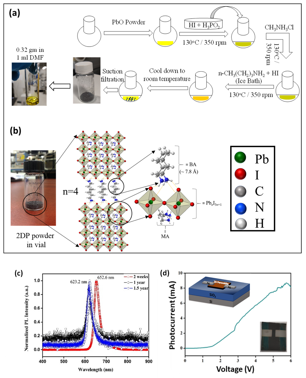
2.2. Comparative Characterization of 3D and 2D PSCs

After our electronic transport measurements on the synthesized 2DP films, we then proceeded toward their integration in the PSC fabrication process, and alongside we also prepared our 3DP (MAPBI3) films for comparative analysis. Both films were formed on top of FTO substrates and their optical properties were studied using PL spectroscopy which was measured using the LabRAM HR Evolution spectrometer (HORIBA Scientific) equipped with a 532 nm excitation laser. Figure 3a shows the PL spectra comparatively for the spin-coated 3DP and 2DP films, where a blue shift in the emission peak for the 2DP film (~739.4 nm) is present, in comparison to the 3DP film (~773.4 nm) which corresponds to ~1.67 eV and ~1.60 eV, respectively. We also characterized the 3DP and 2DP films using UV-Vis optical absorption spectroscopy, measured using the Agilent CARY 5000 spectrophotometer, and the data are shown in Figure 3b,c, respectively. From the absorbance data, the optical bandgap Eg was calculated using the Tauc plot, where (αhυ)2 was plotted as a function of the energy, here υ is the frequency of the incoming light source and h is the Planck’s constant. Using the Tauc equation ( α h v ) n = A ( h v E g ) , the x-intercept to this plot represents the optical Eg. Since organic-inorganic metal halide perovskites are direct bandgap semiconductors, the n was assumed to be 2, and α the absorption coefficient, was calculated using the absorption data according to 2.303 × Absorption Thickness . The thickness of the 3DP was ~400 nm and that of the 2DP film was ~360 nm, based on spinning parameters used. From the linear extrapolation of the plot, the Eg for the 3DP film was determined to be ~1.59 eV, as shown in Figure 3b, while the Eg for the 2DP film was determined to be ~1.67 eV, as shown in Figure 3c. These values are in close agreement with the PL emission peaks which were calculated to be ~1.60 eV and ~1.67 eV, respectively, from the data in Figure 3a.
For extracting the PV device parameters, we fabricated PSCs using the 3DP and 2DP absorbers in the n-i-p architecture, as shown by the schematic in Figure 4a. The working principle in this regular architecture proceeds according to an incoming photon being absorbed within the 2D or 3D absorber layer, and leading to the generation of electron-hole pairs or bound excitons in the active layer. These excitons are then separated and collected in the respective electron transport layer (ETL) and HTL, and subsequently generate a current at the terminals. The deposition and spin coating conditions for the MAPbI3 and ((CH3(CH2)3NH3)2(CH3NH3)3Pb4I13) are summarized in Figure 4b-top and Figure 4b-bottom, respectively. For the 3DP film deposition process illustrated in Figure 4b-top, the one-step solvent exchange process was used with the Lewis-base-acid adduct in 4:1 anhydrous DMF:DMSO with precursors MAI (1.5 M) and PbI2 (1.5 M), while the solution was stirred overnight at RT. Figure 4b-top shows the spinning conditions with an initial 800 rpm for 5 s, followed by 4500 rpm at 20 s using 100 μL solution. For the antisolvent, 0.1 mL of toluene was slowly dripped on the rotating substrate in the last 5 s, which is important for the controlled reaction kinetics and nucleation of the film. The substrate was then transferred to a hotplate for annealing at 125 °C for 30 min. On the other hand, the 2DP ((CH3(CH2)3NH3)2(CH3NH3)3Pb4I13) film was deposited using the hot-casting technique on a pre-heated FTO substrate at ~125 °C, as shown by the film synthesis process flow in Figure 4b-bottom, where the 2DP precursor was deposited at 5000 rpm for 20 s and annealing was conducted at 125 °C for 3 min.
For the n-i-p fabrication process on FTO substrates, c-TiO2 and Spiro-OMeTAD served as the ETL and HTL, respectively, and e-beam evaporated Au was used as the collector electrode. The details of the entire fabrication process and deposition conditions used for the 3D PSC and 2D PSC are shown in Figure 4c-top and Figure 4c-bottom, respectively. The FTO glass substrates (Zhuhai Kaivo/China) were sequentially cleaned by detergent, DI water, and acetone and sonicated with isopropyl alcohol in an ultrasonic bath for 30 min. This was then followed by UV-O3 treatment in a UV-ozone oven for 20 min. After this, we then spin-coated 0.15 M solution of titanium diisopropoxide bis(acetylacetonate) in ethanol at 4000 rpm for 20 s to form a compact titanium dioxide (c-TiO2) layer, which served as the ETL that was subsequently annealed at 510 °C for 30 min. Next, we transferred the TiO2 coated substrates into the glove box and spin coated the MAPbI3 (1.5 M) solution at 800 rpm for 5 s followed by 4500 rpm for 20 s and 0.1 mL of toluene was slowly dripped on the rotating substrate in the last 5 s (as also shown in Figure 4b-top). Then the films were annealed at 125 °C for 30 min. Once the substrates cooled down, spiro-OMeTAD (used as received 2,2′,7,7′-tetrakis-(N,N-di-p-methoxyphenylamine)-9,9′-spirobifluorene from Lumtec) solution was spin coated at 4000 rpm/20 s on top of the 3DP layer as the HTL. Finally, ~80 nm of Au was deposited using e-beam evaporation at a pressure of ~10−5 Torr. The PSC device fabrication process for the 2D PSC is similar and is shown in Figure 4c-bottom. Here, the preheated TiO2 deposited substrate was immediately transferred to the spin coater using the hot-casting approach already discussed, where 0.118 M solution of the 2D precursor in DMF was used and annealed at 125 °C for 3 min. As noted, the rest of the device fabrication process for the 2DP PSC was similar to the 3D PSC fabrication process.
The electrical characteristics of the fabricated PSCs were measured under one-sun optical illumination, i.e., 100 mW-cm−2, using the Oriel LSH-7320 LED solar simulator connected to a source meter unit from Ossila (Model: X200). The light was calibrated with a standard mono-Si solar cell (PVM-396, PV Measurements Inc., Boulder, CO, USA) certified by the US National Renewable Energy Laboratory (NREL). The optimized J-V Characteristic of the 3D PSC is shown in Figure 4d, which resulted in a maximum PCE of ~15.69%, with an open circuit voltage Voc = 1.06 V, short circuit current density Jsc of 21.89 mA-cm−2, and a fill factor of FF = 67.50%. The J-V Characteristic for the 2D PSC is shown in Figure 4e, and a PCE of ~3.33% resulted, with a Voc = 1.13 V, Jsc ~ 5.5 mA-cm−2 and FF = 53.51%. The PV figures of merit for both absorber devices is summarized in Table 1.

2.3. Stability Comparison of 3DP and 2DP Absorbers

To gain insights into the degradation paths related to the 2D and 3D photoabsorbers, we spin coated the 3DP and 2DP absorbers on top of FTO substrates, as shown by the film deposition processes outlined already in Figure 4b, top and bottom, respectively. Their properties were examined as a function of environmental storage using the FEI Quanta environmental SEM, the Rigaku Ultima III X-ray diffractometer for the XRD analysis, and UV-vis spectroscopy. For the SEM analysis, three cases were considered, i.e., (i) freshly deposited films, (ii) films exposed to room temperature ambient (RT) for a duration of 8 h at ~25 °C and ~45 ± 5% RH (uncovered), and (iii) films exposed to ~90% RH using an in-house simulated humidity chamber at ambient temperature of ~25 °C for 30 min. SEM images corresponding to 3DP films are shown in Figure 5a-(i) for freshly deposited films, (ii) ambient (RT) exposed films, and (iii) RH ~90% exposed films. The freshly deposited films in Figure 5a-(i) appear dense, and showed a uniform morphology with a small grain size, which is very well aligned with previous reports. The RT exposed films in Figure 5a-(ii) reveal signs of void formation, particularly at boundaries separating the grains. The increase in porosity and cracking suggests degradation pathways for the 3DP, contributing to its diminished stability. In Figure 5a-(iii),, the films have largely disintegrated, and the substrate was also discolored. Similarly, SEM images corresponding to the 2DP films are shown in Figure 5b-(i) for freshly deposited films, which shows the fresh 2DP film is very uniform, smooth and dense, though some emergent boundary porous regions are evident. In Figure 5b-(ii) the films are exposed to RT ambient for a duration of 8 h at 25 °C and 45 ± 5% RH (uncovered), and Figure 5b-(iii) represents films exposed to RH using an in-house simulated humidity chamber at ambient temperature of ~25 °C for 30 min. In contrast to the 3DP, the 2DP showed an identical surface morphology for both fresh and RT exposed films (Figure 5b-(i,ii)). Thus, unlike the case for the 3DP film, the 2DP film still appears smooth and dense, as noted in Figure 5b-(ii), but the onset of degradation is evident when the 2DP films were exposed to 90% RH, as in Figure 5b-(iii). Regarding the appearance of the two films, the 2DP and 3DP films turned yellow in color upon exposure to a RH of ~90%. However, from the comparative analysis, it appears the 2DP films are denser and smoother and can sustain exposure to moisture-rich ambient conditions, well beyond that possible with our 3DP films.
The XRD analysis for both 3DP and 2DP films was also conducted and the respective XRD spectra are shown in Figure 6a,b. The XRD spectra shown in Figure 6a-(i–iii) for the 3DP films reveals the major diffraction peaks at 2θ ~ 14.1°, 19.98°, 23.42°, 24.5°, 28.46°, and 31.92°, that correspond to the tetragonal perovskite phase indexed to (110), (200), (211), (202), (220), and (310) crystalline planes, respectively, as shown specifically in the freshly deposited films in Figure 6a-(iii). In prior work by Jia et al [61] they examined the bare FTO (220) peak occurring at ~26°, although our (200) peak is present at ~21° and this shift in angular position may have to do with the bare FTO substrate itself interacting with the degraded perovskite. We also note that additional peaks were obtained at lower angles for the 2DP, for example at ~6.7° and ~8.9°, when the films were exposed to the 90% RH condition. These maybe attributable to the lower order crystal planes in the 2DP, i.e., (060) and (080) and their presence may have origins in solvated phases that do not retain their original phase purity and are dissociated into BA+, MA+, and (PbIx)2−x ions. Similarly, the XRD spectra of the 2DP film shown in 6b-(i–iii), reveals the distinct crystallinity of the 2DP films with the two dominant planes at ~14.1°, ~28.41° and also at ~43.1° indexed to the 2D perovskite crystallographic (111), (202) planes and (313) planes, respectively, as shown in Figure 6b-(iii) for the freshly deposited films. As shown in Figure 6a-(iii), fresh films showed characteristic peaks of 3DP, while the 3DP peaks subsided in samples stored at RT (Figure 6a-(ii)). Interestingly for the 2DP films, fresh and lab ambient films (Figure 6b-(ii,iii)) preserved the characteristic peaks in both environmental ambient. Notably, upon exposing both absorbers in RH ~90%, the characteristics peaks diminished for both absorbers which is observed in Figure 6a-(i),b-(i), respectively. Taking the (110) peak and (111) peak for 3DP and 2DP films, respectively, the grain size for the fresh and RT exposed films was calculated using the Scherrer relation, S = K λ β cos θ , where S is the estimated crystalline grain size, λ = 1.5406   Å is the wavelength of the X-rays used in the diffractometer, β is the FWHM in radians, θ is the diffraction Bragg angle, and K is the Scherrer constant or shaping factor. The K value ranges from 0.94, 0.89 for the 3DP films and is ~0.9 for the 2DP films assuming spherical crystallites [52,53,54]. The K for our 3DP and 2DP films was thus taken to be ~0.9, assuming spherical crystals likely for our samples, which is within the 0.89 and 0.94 range. These values of S were computed and are summarized in Table 2 for both fresh and RT exposed 3DP and 2DP films, where S ~ 15.2 nm for 3DP-fresh which increased to ~30.1 nm when the films were exposed to RT. This is consistent with the SEM images in Figure 5a-(ii), where increased porosity of the films is clearly visible in the SEM images. On the contrary, for the 2DP films, S ~ 29.4 nm for fresh films and when the samples were exposed to RT, the S ~16.18 nm. The porosity of the film is not greatly altered in these samples, which is reflected in the SEM images shown in Figure 5b-(ii). Thus, the increased porosity at grain boundaries in the 3DP manifests itself as potential degradation pathways for the RT exposed films, supporting their diminished stability, in contrast to the 2DP, which is largely unchanged morphologically through the correlations we have made using SEM and XRD data.
Besides the morphology and structural characterization conducted above, we also performed UV-Vis optical absorption spectroscopy on both the 3DP and 2DP films on top of FTO substrates for three environmental ambients to gauge stability. The onset of the optical absorption edge for the 3DP freshly synthesized film occurs at ~775 nm, as shown by the data in Figure 7a. On the other hand, this absorption edge starts at a shorter λ, less than 700 nm for the 2DP film in Figure 7b. For the RT exposed 3DP samples in Figure 7a, there is already a reduction in the absorbance below 625 nm, while for the RT exposed 2DP samples in Figure 7b, an improvement in the absorbance is seen for all wavelengths in the measurement range below the optical absorption edge, i.e., <700 nm, suggesting that the 2DP is performing optimally as a photoabsorber and is more stable at these environmental conditions. For the 3DP exposed to RH ~90%, there is once again a general reduction in the optical absorption based on the intensity, and a sharp rising edge occurs at λ < 525 nm, which maybe attributable to the breakdown of the 3DP film into PbI2 that is optically active at shorter λ, closer to the near-UV region. Equivalently, for the 2DP film, several optical resonances surface between 550–650 nm at all of the three environmental conditions examined, which are not evident in the spectra of the 3DP film. The optical resonances in the 2DP films may be attributable to quantum confinement and excitonic effects given the reduced physical dimension of the 2DP structure based on the crystalline lattice. From the summary of the optical absorption spectroscopy data, it is clear the 2DP film is more stable upon exposure to moisture-rich environments, compared to the 3DP film whose optical absorption spectra shows a steady decline in the environmental ambients tested, compared to the freshly deposited films.

3. Conclusions

In summary, we characterized the photoresponse of reduced dimensionality (BA)2(MA)3Pb4I13 2DP crystallites, where the photocurrent and responsivity were measured as a function of wavelength at room temperature. The synthesized 2DP was compared with the 3DP MAPbI3 absorber and the bandgap of both the MAPbI3 and 2DRP was determined to be ~1.6 eV and ~1.67 eV, respectively, based on the PL emission spectra and equivalent values for Eg were determined to be ~1.59 eV for MAPbI3 and 1.67 eV for 2DP using the Tauc approach, respectively. The PV device figures of merit for the 2DP and 3DP absorbers in the n-i-p architecture on FTO substrates were also extracted and compared. We then conducted a comparative material stability analysis in elevated moisture ambients, where the fresh films, ambient exposed films (RT and RH > 90%) were examined using SEM, XRD, and UV-Vis and all of our material probes indicated that the 2DP films were more robust upon exposure to elevated moisture levels, though degradation in RH 90% ambients caused both films to degrade. Thus, we validated the increased stability of 2DP compared to the 3DP based on environmental storage conditions.

Author Contributions

Conceptualization, A.B.K.; Experimental Methodology, A.B.K., K.K., S.A., M.T. and M.S.; Results Analysis and Discussion, K.K., S.A., M.T., M.S. and A.B.K.; writing—original draft preparation, S.A., M.T. and K.K.; writing—review and editing, A.B.K., S.A., M.T., K.K. and M.S.; supervision, A.B.K.; project administration, A.B.K.; funding acquisition, A.B.K. All authors have read and agreed to the published version of the manuscript.

Funding

This research was funded by the Office of Naval Research (ONR) (Grant No. N00014-20-1-2597).

Institutional Review Board Statement

Not applicable.

Informed Consent Statement

Not applicable.

Data Availability Statement

The data presented in this study are available on request from the corresponding author.

Acknowledgments

We thank the Office of Naval Research (grant number ONR N00014-20-1-2597) that enabled us to pursue this work. A.B.K. is also grateful to the support from the PACCAR Technology Institute at UNT.

Conflicts of Interest

The authors declare no conflict of interest.

References

  1. Yin, W.J.; Shi, T.; Yan, Y. Unique properties of halide perovskites as possible origins of the superior solar cell performance. Adv. Mater. 2014, 26, 4653. [Google Scholar] [CrossRef] [PubMed]
  2. Snaith, H. Perovskites: The emergence of a new era for low-cost, high-efficiency solar cells. J. Phys. Chem. Lett. 2013, 4, 3623. [Google Scholar] [CrossRef]
  3. Kojima, A.; Teshima, K.; Shirai, Y.; Miyasaka, T. Organometal Halide Perovskites as Visible-Light Sensitizers for Photovoltaic Cells. J. Am. Chem. Soc. 2009, 131, 6050. [Google Scholar] [CrossRef] [PubMed]
  4. Schmidt-Mende, L.; Dyakonov, V.; Olthof, S.; Ünlü, F.; Lê, K.M.T.; Mathur, S.; Karabanov, A.D.; Lupascu, D.C.; Herz, L.M.; Hinderhofer, A.; et al. Roadmap on organic inorganic hybrid perovskite semiconductors and devices. APL Mater. 2021, 9, 109202. [Google Scholar] [CrossRef]
  5. Savenije, T.J.; Ponseca, C.S.; Kunneman, L.; Abdellah, M.; Zheng, K.; Tian, Y.; Zhu, Q.; Canton, S.E.; Scheblykin, I.G.; Pullerits, T.; et al. Thermally Activated Exciton Dissociation and Recombination Control the Carrier Dynamics in Organometal Halide Perovskite. J. Phys. Chem. Lett. 2014, 5, 2189. [Google Scholar] [CrossRef]
  6. Stranks, S.D.; Eperon, G.E.; Grancini, G.; Menelaou, C.; Alcocer, M.J.P.; Leijtens, T.; Herz, L.M.; Petrozzaand, A.; Snaith, H.J. Electron-Hole Diffusion Lengths Exceeding 1 Micrometer in an Organometal Trihalide Perovskite Absorber. Science 2013, 342, 341–344. [Google Scholar] [CrossRef]
  7. Dong, Q.; Fang, Y.; Shao, Y.; Mulligan, P.; Qiu, J.; Cao, L.; Huang, J. Electron-hole diffusion lengths > 175 μm in solution-grown CH3NH3PbI3 single crystals. Science 2015, 347, 967. [Google Scholar] [CrossRef]
  8. Wetzelaer, G.J.A.H.; Scheepers, M.; Sempere, A.M.; Momblona, C.; Ávila, J.; Bolink, H.J. Trap-Assisted Non-Radiative Recombination in Organic–Inorganic Perovskite Solar Cells. Adv. Mater. 2015, 27, 1837. [Google Scholar] [CrossRef]
  9. Nazeeruddin, M.K.; Snaith, H. Methylammonium lead triiodide perovskite solar cells: A new paradigm in photovoltaics. MRS Bull. 2015, 40, 641. [Google Scholar] [CrossRef]
  10. Jiang, J.; Sun, X.; Chen, X.; Wang, B.; Chen, Z.; Hu, Y.; Guo, Y.; Zhang, L.; Ma, Y.; Gao, L.; et al. Carrier lifetime enhancement in halide perovskite via remote epitaxy. Nat. Commun. 2019, 10, 4145. [Google Scholar] [CrossRef] [Green Version]
  11. Alarousu, E.; El-Zohry, A.M.; Yin, J.; Zhumekenov, A.A.; Yang, C.; Alhabshi, E.; Gereige, I.; AlSaggaf, A.; Malko, A.V.; Bakr, O.M.; et al. Ultralong Radiative States in Hybrid Perovskite Crystals: Compositions for Submillimeter Diffusion Lengths. J. Phys. Chem. Lett. 2017, 8, 4386. [Google Scholar] [CrossRef] [PubMed]
  12. Mykhaylyk, V.B.; Kraus, H.; Kapustianyk, V.; Kim, H.J.; Mercere, P.; Rudko, M.; da Silva, P.; Antonyak, O.; Dendebera, M. Bright and fast scintillations of an inorganic halide perovskite CsPbBr3 crystal at cryogenic temperatures. Sci. Rep. 2020, 10, 8601. [Google Scholar] [CrossRef] [PubMed]
  13. Chen, Q.; Zhou, H.; Fang, Y.; Stieg, A.Z.; Song, T.B.; Wang, H.H.; Xu, X.; Liu, Y.; Lu, S.; You, J.; et al. The optoelectronic role of chlorine in CH3NH3PbI3 (Cl)-based perovskite solar cells. Nat. Commun. 2015, 6, 7269. [Google Scholar] [CrossRef] [PubMed]
  14. Best Research-Cell Efficiencies. Available online: www.nrel.gov/ncpv/images/efficiencychart.jpg (accessed on 30 June 2022).
  15. Pacchioni, G. Highly efficient perovskite LEDs. Nat. Rev. Mater. 2021, 6, 108. [Google Scholar] [CrossRef]
  16. Fan, J.; Du, W.; Mi, Y.; Liu, X. Perovskite-based lasers: An introductory survey. In Nanoscale Semiconductor Lasers; Elsevier: Amsterdam, The Netherlands, 2019; pp. 41–47. [Google Scholar]
  17. Deng, W.; Zhang, X.; Huang, L.; Xu, X.; Wang, L.; Wang, J.; Shang, Q.; Lee, S.T.; Jie, J. Aligned Single-Crystalline Perovskite Microwire Arrays for High-Performance Flexible Image Sensors with Long-Term Stability. Adv. Mater. 2016, 28, 2201. [Google Scholar] [CrossRef]
  18. Li, C.H.A.; Zhou, Z.; Vashishtha, P.; Halpert, J.E. The Future Is Blue (LEDs): Why Chemistry Is the Key to Perovskite Displays. Chem. Mater. 2019, 31, 6003. [Google Scholar] [CrossRef]
  19. Kennard, R.M.; Dahlman, C.J.; Morgan, E.E.; Chung, J.; Cotts, B.L.; Kincaid, J.R.; DeCrescent, R.A.; Stone, K.H.; Panuganti, S.; Mohtashami, Y.; et al. Enhancing and Extinguishing the Different Emission Features of 2D (EA1−xFAx)4Pb3Br10 Perovskite Films. Adv. Opt. Mater. 2022. [Google Scholar] [CrossRef]
  20. Liu, J.; Xue, Y.; Wang, Z.; Xu, Z.Q.; Zheng, C.; Weber, B.; Song, J.; Wang, Y.; Lu, Y.; Zhang, Y.; et al. Two-dimensional CH3NH3PbI3 perovskite: Synthesis and optoelectronic application. ACS Nano 2016, 10, 3536. [Google Scholar] [CrossRef]
  21. Qi, X.; Zhang, Y.; Ou, Q.; Ha, S.T.; Qiu, C.W.; Zhang, H.; Bao, Q.; Cheng, Y.B.; Xiong, Q. Photonics and optoelectronics of 2D metal-halide perovskites. Small 2018, 14, 1800682. [Google Scholar] [CrossRef]
  22. Lee, M.M.; Teuscher, J.; Miyasaka, T.; Murakami, T.N.; Snaith, H.J. Efficient hybrid solar cells based on meso-superstructured ogranometal halide perovskites. Science 2012, 338, 643. [Google Scholar] [CrossRef] [Green Version]
  23. Kim, Y.H.; Cho, H.; Heo, J.H.; Kim, T.S.; Myoung, N.; Lee, C.L.; Im, S.H.; Lee, T.W. Multicolored organic/inorganic hybrid perovskite light-emitting diodes. Adv. Mater. 2015, 27, 1248. [Google Scholar] [CrossRef]
  24. Jacobsson, T.J.; Hultqvist, A.; García-Fernández, A.; Anand, A.; Al-Ashouri, A.; Hagfeldt, A.; Crovetto, A.; Abate, A.; Ricciardulli, A.G.; Vijayan, A.; et al. An open-access database and analysis tool for perovskite solar cells based on the FAIR data principles. Nat. Energy 2022, 7, 107–115. [Google Scholar] [CrossRef]
  25. Sherafatipour, G.; Benduhn, J.; Patil, B.R.; Ahmadpour, M.; Spoltore, D.; Rubahn, H.G.; Vandewal, K.; Madsen, M. Degradation pathways in standard and inverted DBP-C70 based organic solar cells. Sci. Rep. 2019, 9, 4024. [Google Scholar] [CrossRef] [PubMed]
  26. Wang, D.; Wright, M.; Elumalai, N.K.; Uddin, A. Stability of perovskite solar cells. Sol. Energy Mater. Sol. Cells 2016, 147, 255. [Google Scholar] [CrossRef]
  27. Wang, R.; Mujahid, M.; Duan, Y.; Wang, Z.K.; Xue, J.; Yang, Y. A review of perovskites solar cell stability. Adv. Funct. Mater. 2019, 29, 1808843. [Google Scholar] [CrossRef]
  28. Berhe, T.A.; Su, W.N.; Chen, C.H.; Pan, C.J.; Cheng, J.H.; Chen, H.M.; Tsai, M.C.; Chen, L.H.; Dubale, A.A.; Hwang, B.J.; et al. Organometal halide perovskite solar cells: Degradation and stability. Energy Environ. Sci. 2016, 9, 323. [Google Scholar] [CrossRef]
  29. You, J.; Meng, L.; Song, T.B.; Guo, T.F.; Yang, Y.M.; Chang, W.H.; Hong, Z.; Chen, H.; Zhou, H.; Chen, Q.; et al. Improved air stability of perovskite solar cells via solution-processed metal oxide transport layers. Nat. Nanotechnol. 2016, 11, 75. [Google Scholar] [CrossRef]
  30. Wali, Q.; Iftikhar, F.J.; Khan, M.E.; Ullah, A.; Iqbal, Y.; Jose, R. Advances in stability of perovskite solar cells. Org. Electron. 2020, 78, 105590. [Google Scholar] [CrossRef]
  31. He, R.; Ren, S.; Chen, C.; Yi, Z.; Luo, Y.; Lai, H.; Wang, W.; Zeng, G.; Hao, X.; Wang, Y.; et al. Wide-bandgap organic–inorganic hybrid and all-inorganic perovskite solar cells and their application in all-perovskite tandem solar cells. Energy Environ. Sci. 2021, 14, 5723–5759. [Google Scholar] [CrossRef]
  32. Kim, M.; Motti, S.G.; Sorrentino, R.; Petrozza, A. Enhanced solar cell stability by hygroscopic polymer passivation of metal halide perovskite thin film. Energy Environ. Sci. 2018, 11, 2609. [Google Scholar] [CrossRef]
  33. Abdelmageed, G.; Mackeen, C.; Hellier, K.; Jewell, L.; Seymour, L.; Tingwald, M.; Carter, S. Effect of temperature on light induced degradation in methylammonium lead iodide perovskite thin films and solar cells. Sol. Energy Mater. Sol. Cells 2018, 174, 566. [Google Scholar] [CrossRef]
  34. Yang, Y.; Yuan, Q.; Li, H.; Niu, Y.; Han, D.; Yang, Q.; Feng, L. Dopant free mixture of Spiro-OMeTAD and PTAA with tunable wettability as hole transport layer enhancing performance of inverted CsPbI₂Br perovskite solar cells. Org. Electron. 2020, 86, 105873. [Google Scholar] [CrossRef]
  35. Zhou, C.; Tarasov, A.B.; Goodilin, E.A.; Chen, P.; Wang, H.; Chen, Q. Recent strategies to improve moisture stability in metal halide perovskites materials and devices. J. Energy Chem. 2022, 65, 219. [Google Scholar] [CrossRef]
  36. Gao, P.; Yusoff, A.R.B.M.; Nazeeruddin, M.K. Dimensionality engineering of hybrid halide perovskite light absorbers. Nat. Commun. 2018, 9, 5028. [Google Scholar] [CrossRef] [PubMed]
  37. Ke, W.; Stoumpos, C.C.; Zhu, M.; Mao, L.; Spanopoulos, I.; Liu, J.; Kontsevoi, O.Y.; Chen, M.; Sarma, D.; Zhang, Y.; et al. Enhanced photovoltaic performance and stability with a new type of hollow 3D perovskite {en} FASnI3. Sci. Adv. 2017, 3, e1701293. [Google Scholar] [CrossRef] [PubMed]
  38. Zhang, H.; Ren, X.; Chen, X.; Mao, J.; Cheng, J.; Zhao, Y.; Liu, Y.; Milic, J.; Yin, W.J.; Grätzel, M.; et al. Improving the stability and performance of perovskite solar cells via off-the-shelf post-device ligand treatment. Energy Environ. Sci. 2018, 11, 2253. [Google Scholar] [CrossRef]
  39. Ren, A.; Lai, H.; Hao, X.; Tang, Z.; Xu, H.; Jeco, B.M.F.Y.; Watanabe, K.; Wu, L.; Zhang, J.; Sugiyama, M.; et al. Efficient perovskite solar modules with minimized nonradiative recombination and local carrier transport losses. Joule 2020, 4, 1263–1277. [Google Scholar] [CrossRef]
  40. Roghabadi, F.A.; Alidaei, M.; Mousavi, S.M.; Ashjari, T.; Tehrani, A.S.; Ahmadi, V.; Sadrameli, S.M. Stability progress of perovskite solar cells dependent on the crystalline structure: From 3D ABX 3 to 2D Ruddlesden–Popper perovskite absorbers. J. Mater. Chem. A 2019, 7, 5898. [Google Scholar] [CrossRef]
  41. Li, N.; Zhu, Z.; Chueh, C.C.; Liu, H.; Peng, B.; Petrone, A.; Li, X.; Wamg, L.; Jen, A.K.Y. Mixed cation FAxPEA1–xPbI3 with enhanced phase and ambient stability toward high-performance perovskite solar cells. Adv. Energy Mater. 2017, 7, 1601307. [Google Scholar] [CrossRef]
  42. Stoumpos, C.C.; Malliakas, C.D.; Kanatzidis, M.G. Semiconducting tin and lead iodide perovskites with organic cations: Phase transitions, high mobilities, and near-infrared photoluminescent properties. Inorg. Chem. 2013, 52, 9019. [Google Scholar] [CrossRef]
  43. Stoumpos, C.C.; Kanatzidis, M.G. The renaissance of halide perovskites and their evolution as emerging semiconductors. Acc. Chem. Res. 2015, 48, 2791. [Google Scholar] [CrossRef] [PubMed]
  44. Tsai, H.; Nie, W.; Blancon, J.C.; Stoumpos, C.C.; Asadpour, R.; Harutyunyan, B.; Mohite, A.D. High-efficiency two-dimensional Ruddlesden–Popper perovskite solar cells. Nature 2016, 536, 312. [Google Scholar] [CrossRef] [PubMed]
  45. Blancon, J.C.; Tsai, H.; Nie, W.; Stoumpos, C.C.; Pedesseau, L.; Katan, C.; Kepenekian, M.; Soe, C.M.M.; Appavoo, K.; Sfeir, M.Y.; et al. Extremely efficient internal exciton dissociation through edge states in layered 2D perovskites. Science 2017, 355, 1288. [Google Scholar] [CrossRef]
  46. Li, W.; Sidhik, S.; Traore, B.; Asadpour, R.; Hou, J.; Zhang, H.; Fehr, A.; Essman, J.; Wang, Y.; Hoffman, J.M.; et al. Light-activated interlayer contraction in two-dimensional perovskites for high-efficiency solar cells. Nat. Nanotechnol. 2022, 17, 45. [Google Scholar] [CrossRef]
  47. Protesescu, L.; Yakunin, S.; Bodnarchuk, M.I.; Krieg, F.; Caputo, R.; Hendon, C.H.; Yang, R.X.; Walsh, A.; Kovalenko, M.V. Nanocrystals of cesium lead halide perovskites (CsPbX3, X = Cl, Br, and I): Novel optoelectronic materials showing bright emission with wide color gamut. Nano Lett. 2015, 15, 3692. [Google Scholar] [CrossRef]
  48. Akkerman, Q.A.; D’Innocenzo, V.; Accornero, S.; Scarpellini, A.; Petrozza, A.; Prato, M.; Manna, L. Tuning the optical properties of cesium lead halide perovskite nanocrystals by anion exchange reactions. J. Am. Chem. Soc. 2015, 137, 10276. [Google Scholar] [CrossRef] [PubMed]
  49. Novoselov, K.S.; Geim, A.K.; Morozov, S.V.; Jiang, D.; Zhang, Y.; Dubonos, S.V.; Grigorieva, I.V.; Firsov, A.A. Electric Field Effect in Atomically Thin Carbon Films. Science 2004, 306, 666. [Google Scholar] [CrossRef] [PubMed]
  50. Kaul, A.B. Two-dimensional layered materials: Structure, properties, and prospects for device applications. J. Mater. Res. 2014, 29, 348. [Google Scholar] [CrossRef]
  51. Chen, Y.; Sun, Y.; Peng, J.; Tang, J.; Zheng, K.; Liang, Z. 2D Ruddlesden–Popper Perovskites for Optoelectronics. Adv. Mater. 2018, 30, 1703487. [Google Scholar] [CrossRef]
  52. Stoumpos, C.C.; Cao, D.H.; Clark, D.J.; Young, J.; Rondinelli, J.M.; Jang, J.I.; Hupp, J.T.; Kanatzidis, M.G. Ruddlesden–Popper Hybrid Lead Iodide Perovskite 2D Homologous Semiconductors. Chem. Mater. 2016, 28, 2852. [Google Scholar] [CrossRef]
  53. Min, M.; Hossain, R.F.; Adhikari, N.; Kaul, A.B. Inkjet-Printed Organohalide 2D Layered Perovskites for High-Speed Photodetectors on Flexible Polyimide Substrates. ACS Appl. Mater. Interfaces 2020, 12, 10809. [Google Scholar] [CrossRef] [PubMed]
  54. Hossain, R.F.; Min, M.; Ma, L.C.; Sakri, S.R.; Kaul, A.B. Carrier photodynamics in 2D perovskites with solution-processed silver and graphene contacts for bendable optoelectronics. NPJ 2D Mater. Appl. 2021, 5, 34. [Google Scholar] [CrossRef]
  55. Liu, B.; Soe, C.M.M.; Stoumpos, C.C.; Nie, W.; Tsai, H.; Lim, K.; Mohite, A.D.; Kanatzidis, M.G.; Marks, T.J.; Singer, K.D. Optical properties and modeling of 2D perovskite solar cells. Sol. RRL 2017, 1, 1700062. [Google Scholar] [CrossRef]
  56. Leguy, A.M.; Azarhoosh, P.; Alonso, M.I.; Campoy-Quiles, M.; Weber, O.J.; Yao, J.; Bryant, D.; Weller, M.T.; Nelson, J.; Walsh, A.; et al. Experimental and theoretical optical properties of methylammonium lead halide perovskites. Nanoscale 2016, 8, 6317. [Google Scholar] [CrossRef]
  57. Liang, X.; Baker, R.W.; Wu, K.; Deng, W.; Ferdani, D.; Kubiak, P.S.; Marken, F.; Torrente-Murciano, L.; Cameron, P.J. Continuous low temperature synthesis of MAPbX3 perovskite nanocrystals in a flow reactor. React. Chem. Eng. 2018, 3, 640. [Google Scholar] [CrossRef]
  58. El-Henawey, M.I.; Gebhardt, R.S.; El-Tonsy, M.M.; Chaudhary, S. Organic solvent vapor treatment of lead iodide layers in the two-step sequential deposition of CH3NH3PbI3-based perovskite solar cells. J. Mater. Chem. A Mater. Energy Sustain. 2016, 4, 1947. [Google Scholar] [CrossRef]
  59. Sidhik, S.; Li, W.; Samani, M.H.; Zhang, H.; Wang, Y.; Hoffman, J.; Mohite, A.D.; Fehr, A.K.; Wong, M.S.; Katan, C.; et al. Memory Seeds Enable High Structural Phase Purity in 2D Perovskite Films for High-Efficiency Devices. Adv. Mater. 2021, 33, 2007176. [Google Scholar] [CrossRef]
  60. Xing, J.; Zhao, Y.; Askerka, M.; Quan, L.N.; Gong, X.; Zhao, W.; Zhao, J.; Tan, H.; Long, G.; Gao, L.; et al. Color-stable highly luminescent sky-blue perovskite light-emitting diodes. Nat. Commun. 2018, 9, 1–8. [Google Scholar] [CrossRef]
  61. Jia, E.D.; Lou, X.; Zhou, C.L.; Hao, W.C.; Wang, W.J. O3 fast and simple treatment-enhanced p-doped in Spiro-MeOTAD for CH3NH3I vapor-assisted processed CH3NH3PbI3 perovskite solar cells. Chin. Phys. B 2017, 26, 068803. [Google Scholar] [CrossRef]
Figure 1. (a) Synthesis process of 2DP ((CH3(CH2)3NH3)2(CH3NH3)3Pb4I13) powder using the precursors shown. (b) Synthesized 2DP powder in a vial (left), and the concomitant crystalline structure for the n = 4 formulation (right). (c) The inherent stability of the 2DP powder was gauged using steady-state PL measurements, gathered over the course of 1.5 years, for crystals stored at ambient temperatures in a desiccator. A slight blue shift of 29 nm in the peak position with time was evident, but the crystals were still photoactive with a well-defined emission peak, and a FWHM that was largely unchanged over the 1.5 years of observation time. (d) The 2DP crystals were dispersed in solution and spin cast into thin films on an oxidized Si substrate with metal electrodes that were deposited using a shadow mask. Here the Ip was measured as a function of voltage and the top inset shows the schematic of the device, with the fabricated version of the device seen in the bottom inset.
Solar 02 00023 g001
Figure 2. (a) The Ip was measured as a function of λ over the 400 to 1100 nm spectral range for the 2DP film photoabsorber where the peak in Ip occurring at ~775 nm was consistent with the peak position of the PL emission spectrum for our n = 4, 2DP formulation. (b) Responsivity R as a function of λ over the same spectral range, and again, the highest R coincided with the PL peak emission observed in our 2DP photoabsorber. The laser power used was ~200 µW and the laser spot size of the fiber optic cable irradiating our device defined an active area of ~5 µm2.
Solar 02 00023 g002
Figure 3. (a) The steady state PL spectra for our 2DP and 3DP films deposited directly on unetched FTO/glass substrates, which shows a peak emission occurring at 1.60 eV for the 3DP film and a peak position occurring at 1.67 eV for the 2DP photoabsorber. From the absorbance data measured using UV-Vis optical absorption spectroscopy, the optical bandgap Eg was determined using the Tauc approach for the (b) 3DP film, and the (c) 2DP film, where Eg was determined to be ~1.59 eV and 1.67 eV, respectively; these results were largely in alignment with the PL emission data.
Solar 02 00023 g003
Figure 4. (a) The n-i-p architecture was used for our 3DP (MAPbI3) and 2DP (CH3(CH2)3NH3)2(CH3NH3)3Pb4I13 PSC fabrication process. (b) Deposition procedure and conditions used for the 3DP (top) and 2DP (bottom) thin films. (c) Fabrication process and deposition conditions used for the entire 3D PSC (top) and 2D PSC (bottom) process. (d) 3DP PSC, where a PCE ~15.69% was achieved, and for the (e) 2DP PSC, where the PCE was measured to be ~3.33%. The other device figures of merit are summarized in Table 1.
Solar 02 00023 g004
Figure 5. Surface morphology characterization studies conducted on spin coated 3DP and 2DP on top of FTO substrates for three cases, (i) freshly deposited films at t = 0, (ii) exposed to room temperature ambient (RT) for a duration of 8 h at 25 °C and 45 ± 5% RH (uncovered), and (iii) exposed to 90% RH in an inhouse simulated humidity chamber at ambient temperatures for 30 min. SEM images corresponding to 3DP films that are (a)-(i) freshly deposited, (ii) ambient RT exposed, and (iii) exposed to RH > 90%. While the freshly deposited films in (a)-(i) appear dense, the RT exposed films in (a)-(ii) reveal signs of void formation, particularly at boundaries separating the grains, while in (a)-(iii), the films have disintegrated, and the substrate is also discolored. SEM image corresponding to 2DP films that are (b)-(i) freshly deposited, (ii) ambient RT exposed, and (iii) exposed to RH > 90%. Unlike the case for the 3DP film, the 2DP film still appears smooth and dense in (ii) after it is freshly formed in (i), but the onset of degradation is evident when the 2DP films are exposed to 90% RH (iii). However, from the comparative analysis, it appears the 2DP films are denser and smoother and can sustain exposure to ambient conditions, well beyond that possible with the 3DP films.
Solar 02 00023 g005
Figure 6. XRD analysis of (a) 3DP and (b) 2DP films. The films in (a)-(i) and (b)-(i) are exposed to 90% RH for 30 min., (a)-(ii) and (b)-(ii) exposed to RT for 8 h, and (a)-(iii) and (b)-(iii) at t = 0 for freshly deposited films; further details on the specific environmental conditions are provided in the caption of Figure 5. For the 3DP films, the amplitude of the (110) peak is diminished significantly even upon exposure to the RT conditions in (ii), while for the 2DP film the (111) peak is strongly active even after exposure to the conditions in (ii). From the (110) and the (111) peaks for the 3DP and 2DP films, respectively, the grain size S at t = 0 for freshly deposited films and RT exposed samples was computed using the Scherrer formula and the data are summarized in Table 2.
Solar 02 00023 g006
Figure 7. UV-vis optical absorption measurements on spin coated (a) 3DP and (b) 2DP films on top of FTO substrates at the three conditions noted in the caption of Figure 5. The onset of the optical absorption edge for the 3DP freshly synthesized film at t = 0 occurs at ~775 nm in (a), while this absorption edge starts at a shorter λ, less than 700 nm for the 2DP film in (b). For the RT exposed 3DP samples in (a), there is already a reduction in the absorbance below 625 nm, while for the RT exposed 2DP samples in (b), an improvement in the absorbance is seen for all wavelengths in the measurement range below the optical absorption edge, i.e., <700 nm. For the 3DP exposed to RH, there is once again a general reduction in the optical absorption based on the intensity, and a sharp rising edge occurs at λ < 525 nm which maybe attributable to the breakdown of the 3DP film into PbI2 which is optically active at shorter λ, closer to the near-UV region. Equivalently, for the 2DP film, several optical resonances surface between 550–650 nm at all of the three environmental conditions examined, which are not present in the spectra of the 3DP film. The optical resonances in the 2DP films may be attributable to quantum confinement and excitonic effects given the reduced physical dimension of the 2DP crystalline structure.
Solar 02 00023 g007
Table 1. Summary of optimized photovoltaic parameters used for the n-i-p PSCs fabricated, as shown in Figure 4, based on the 3DP (MAPbI3) and 2DP ((CH3(CH2)3NH3)2(CH3NH3)3Pb4I13) solar cell absorbers.
PSC AbsorbersVoc (V)Jsc (mA-cm−2)FF (%)PCE (%)Rsh (kΩ-cm2)Rs (Ω-cm2)
3DP1.0621.8967.5015.69913.547.53
2DP1.135.553.513.331159.4243.47
Table 2. The grain size S for the fresh and RT exposed samples was computed using the Scherrer formula from the (110) and the (111) peaks for the 3DP and 2DP films, respectively.
Filmsθ (Degrees)β (Radian)S (nm)
3DP-Fresh7.050.0091915.20
3DP-RT7.030.0046430.10
2DP-Fresh7.050.0047529.41
2DP-RT7.080.0086316.18
Publisher’s Note: MDPI stays neutral with regard to jurisdictional claims in published maps and institutional affiliations.

