Abstract
The effect of foam-like 3D graphene (3DG) in an electron transport material (ETM), viz. ZnO thin film, on the steady-state photoluminescence (PL), light-harvesting efficiency (LHE), photocurrent density (JSC), photovoltage (VOC), and charge transport parameters of perovskite solar cells (PSCs) are systematically investigated. The ETM is developed by spin coating a ZnO precursor solution containing varying amounts of 3DG on conducting glass substrates and appropriate annealing. A significant improvement in the photoconversion efficiency of PSCs is observed for a low concentration of 3DG in ZnO. The current–voltage and electrochemical impedance spectroscopy measurements show that the addition of 3DG enhances the VOC due to efficient electron–hole separation and charge transport compared to the pristine ZnO. These studies offer a route for further advances in enhancing the optoelectronic properties of ETM for artificial photosynthesis and photocatalysis devices.
1. Introduction
Ever since the first introduction of next-generation perovskite solar cell (PSC) by Kojima et al. in 2009, Reference [1] a rapid development in organometallic perovskite-based solar cells were carried out to push the efficiency from 3.81% to over 25% [2,3,4]. A roadmap of PSCs has recently been published [5]. It is of paramount importance to control the PSC material interfacial connection in order to lower the electron–hole recombination, prolong the excited electron life time, and eventually increases the current–density and photovoltage [6,7]. As such, various potential electron-transporting materials (ETMs) were developed such as the commonly known TiO2, ZnO, SnO2, PCBM, and other more complex materials [4,8,9,10,11,12,13,14,15]. With regard to photocurrent extraction, many researchers synthesized TiO2 in the form of thin film, nanotubes, nanoarrays, and other nanostructures as well as doping to reduce the charge recombination and to increase the photocurrent extraction efficiency [16,17,18,19,20]. The combination between TiO2 and carbon fullerenes such as nanotubes and graphene were given much effort for the development of artificial photosynthesis devices [21,22]. Alternatively, ZnO exhibited higher electron mobility compared to TiO2 and better electron extraction capability, which makes it the ETM of choice [23,24,25,26,27]. However, ZnO suffers from such problems as humidity-induced degradation [28,29,30] and high electron–hole recombination compared to the routinely employed TiO2 ETM [31,32,33], despite the former’s many orders of magnitude higher charge mobility through nanostructured films. Many research studies were carried out to lower the electron–hole recombination rate in ZnO by co-doping with noble metal such as Ag [34,35,36,37,38], Au [39,40,41], and Pt [42,43] as well as synthesizing into efficient nanoarrays and core–shell [44,45,46].
The motivation remains the same, which is to improve the effectiveness and consistency of ZnO ETMs. Toward this aim, using a composite of ZnO with graphene as an ETM has also been investigated by several groups [34,35,47,48,49,50]. The unique electronic property of graphene makes it an ideal alternative property modifier for n-type semiconductors such as ZnO and TiO2. Recently, Tavakoli et al. [49,50] and Bagha et al. [34,35] investigated the effect of a reduced graphene oxide (rGO) sheet on the photovoltaic parameters of intrinsic and doped ZnO (Ag and Ni) ETMs in planar PSCs and showed that the rGO sheets passivate the trap states in ZnO on both cases, decrease the charge recombination, and improve charge-carrier extraction efficiency in PSCs. These improvements and increased photoconversion efficiency (PCE) are most likely due to graphene bonding with the surface atoms and subsequent stabilization of the structure, as shown in other electrochemical systems [51]. However, excessive graphene becomes recombination centers, which affect the efficiency of the cell [13]. The graphene layer was also used as an interfacial barrier between ZnO and perovskites; thereby, it was shown to limit the thermal instability between the two interfaces during the annealing process [50]. So far, in these reports, graphene or rGO in a 2D structure and nanoparticles synthesized via chemical vapor deposition or chemical reduction are only considered. Graphene aerogels exhibit enhanced mechanical properties with a very low density that show outstanding resilience and can fully recover after more than 90% compression [52].
In this article, a new approach of dispersing ZnO nanoparticles on foam-like three-dimensional graphene (3DG) was adopted to see its effect as an ETM in PSCs on their optical and photovoltaic properties. A stunning 100% enhancement in the PCE compared to the ETMs containing pure ZnO is observed. The 3DG content in ZnO thin film has been systematically varied to observe the effect on the steady-state photoluminescence (PL), light-harvesting efficiency (LHE), photocurrent density (JSC), and photovoltage (VOC). The effect of 3DG concentration in the ZnO nanoparticles was also studied by incident photon to current conversion efficiency (IPCE) spectroscopy where the addition of 3DG enhances the photovoltage (VOC) [53], which indicates high electron–hole separation and efficient charge transport compared to pristine ZnO. The highest value of 1.0 V was reported for the ZnO-3DG 0.25 based PSCs. The highest value of VOC is due to the lower series resistance and the higher short circuit resistance. Our optimized 3DG-doped ZnO PSCs delivered a maximum PCE enhancement of 112% compared to pristine ZnO PSCs. Therefore, the enhancement of PCE is attributed to the improved VOC, LHE, and charge separation mechanisms within the ZnO-3DG interfaces. These studies offer a route for further advances in enhancing the optoelectronic properties of ETM for artificial photosynthesis and photocatalysis devices.
2. Experimental Details
The ZnO was prepared as reported elsewhere [54] on patterned fluorine doped tin oxide (FTO) glass using a laser scriber. The patterned FTO was cleaned ultrasonically in deionized (DI) water, acetone, and ethanol in sequential manner. Briefly, zinc acetate dehydrate (≈2.195 g) was dissolved in ethanol (50 mL) and stirred vigorously at 60 °C for 30 min. The monoethanolamine (MEA) was added dropwise into the mixed solution to stabilize for a 10 min interval for 2 h, and the resulting transparent solution was stored overnight for gelation. The gel was subsequently spun-coated on the patterned and cleaned FTO glass at 3000 rpm in 30 s for obtaining a compact ZnO thin film; the spin-coating procedure was repeated up to three times to obtain a thicker film. The ZnO-coated FTO glass was sintered at 300 °C for 1 h.
The 3DG was synthesized as reported in our previous work [55,56]. A stock solution of 3DG with a concentration of 0.3 mg/mL in ethanol was made by vigorous sonication. The ZnO stock solution was prepared as in the above procedure. The ZnO/3DG solution was prepared by adding an appropriate volume of dispersed 3DG into 3 mL ZnO solution. The required 3DG in wt % was added into four different concentrations, 0.25, 0.5, 0.75, and 1.0 wt %. The different concentrations of ZnO-3DG thin film were obtained by spin coating ZnO-3DG on cleaned FTO glass following the procedure for developing the ZnO films. The spin-coated films were first annealed at 150 °C for 20 min to remove the organic residues and subsequently to 300 °C for 1 h to obtain compact and crystallized ZnO-3DG thin films.
The perovskite films were developed via the two-step deposition method [57]. Firstly, PbI2 powder (≈462 mg) was diluted in 1 mL of dimethylformamide (DMF) to prepare 1M PbI2 and stirred at 70 °C for 2 h. Methyl ammonium iodide (CH3NH3I) solution was prepared by diluting 100 mg in 10 mL of 2-propanol. Then, the PbI2 solution was spin coated at 2000 rpm for 30 s on the FTO glass coated with ZnO-3DG thin films and annealed at 70 °C for 30 min; the resulting films were subsequently cooled to room temperature. Then, the above films were immersed into CH3NH3I solution for 20 s to form CH3NH3PbI3 and annealed at 70 °C for 30 min and subsequently cooled to room temperature. The gold cathode usually used in the PSCs was replaced with the 3DG, which was prepared following our previous report by thermal pressing and mechanical clamping to the device [55]. All the device fabrications were done in a controlled environment at <1% relative humidity and <200 ppm O2 condition. The schematic representation of the 3DG-ZnO thin film preparation is depicted in Figure 1a, and the consequent energy band diagram is shown in Figure 1b.
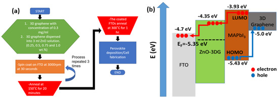
Figure 1.
(a) Schematic representation of 3DG-ZnO nanoparticle thin film synthesis and preparation of devices and (b) energy band diagram of the final device.
The morphology of the ZnO-3DG was determined via field emission scanning electron microscope (FESEM, Zeiss Supra55 VP). Surface chemical states of the samples were obtained by X-ray photoelectron spectroscopy (XPS, Thermo Scientific, Waltham, MA, USA) employing Al-K alpha radiation with a spot size of 400 µm. The phase and crystal structure of the samples were obtained by X-ray diffraction (XRD, X’Pert3, PANalytical Empyrean) measurements employing CuKa radiation. The optical transmittance and absorbance measurements were obtained via UV-Vis absorption spectroscopy (Perkin-Elmer Lambda 950) with a slit width of 2 nm at normal incidence. The photoluminescence spectra of the samples were obtained using Horiba Fluorolog-3, HORIBA Jobin Yvon with an excitation of 600 nm.
The current density–voltage (J-V) curves of the solar cells were measured by a digital source meter (Keithley 2420) under AM 1.5G 1 Sun (100 mW/cm2) irradiation simulated by illumination of 450 W xenon lamp. The solar cells efficiency was obtained from an area of ≈0.1 cm2; the remaining area of the device was adequately masked to minimize straylight effects. The electrochemical impedance spectroscopy (EIS) was employed for studying the charge transport in the device using Gamry Potentiostat under dark. The EIS spectra were recorded with an applied DC voltage ranging from 0 to 1 V with 20 mV AC on DC bias voltage at frequency ranging from 0.1 to 1 MHz. The J-V and EIS characterizations were carried out with >70% humidity and O2 ambient environment.
3. Results and Discussion
The ZnO film incorporated with 3DG was prepared by varying the 3DG concentrations (3DG was added into four different concentration, 0.25, 0.5, 0.75 and 1.0 wt %) in ZnO solution; the samples are abbreviated as ZnO-3DG-(0.25, 0.50, 0.75, and 1.00). The FESEM images of 3DG and ZnO-3DG film are shown in Figure 2. Figure 2a is typical FESEM image of 3DG displaying a large graphene sheet with a 3D morphology. Figure 2b shows the cross-section of ZnO-3DG film developed on FTO, depicting the thickness of the ZnO-3DG film. The film is highly compact and has a thickness of ≈100 nm, and upon close examination, it shows a homogenous surface (Figure 2c), and a magnified view is in Figure 2d. The compactness and uniformity of the thin film is highly critical to prevent direct contact between FTO and the hole transporting material or cathode, which can lead to severe electron–hole recombination [58].
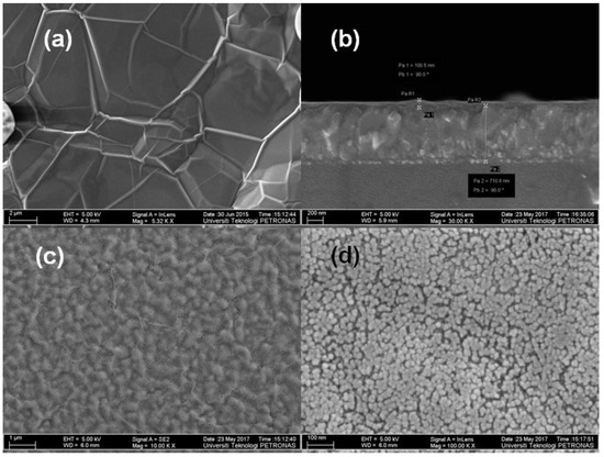
Figure 2.
FESEM images of (a) 3DG film on FTO substrate; (b) cross-section of ZnO-3DG-0.25 film on FTO substrate, (c,d) surface morphology of the ZnO-3DG-0.25 film at different magnifications.
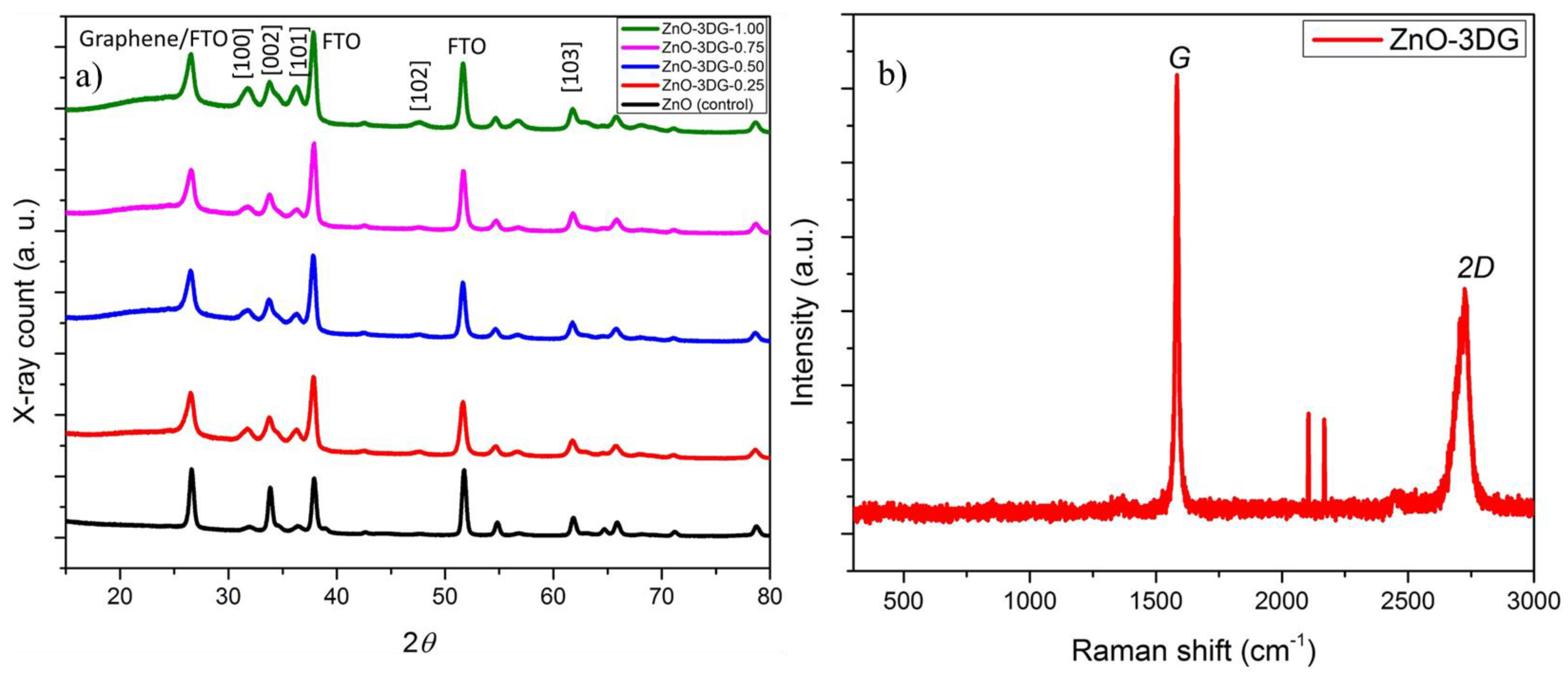
The XRD analyses were conducted for all ZnO-3DG samples to determine the crystal structure and the presence of graphene within the photoanode (Figure 3a). The most prominent peaks of ZnO NPs seen at 31.8° (100), 34.5° (002), and 36.3° (101) are agreeable with the standard JCPDS Card No. 36-1451 for ZnO thin film. Interestingly, the single XRD peak for graphene can be seen for all 3DG incorporated ZnO at 27°, which are dominated by the FTO peak. The small bump before the peak 27° indicates the fingerprint of the graphene peak, which cannot be seen for the pristine ZnO thin film. The average particle sizes of pristine ZnO and ZnO-3DG were calculated using the Scherrer equation , where τ is the average particle size, λ is the X-ray wavelength, β is the line broadening at full-width half-maximum, and θ is the Bragg’s angle. The average particle sizes of pristine ZnO and ZnO-3DG were recorded at ≈22 nm and ≈14 nm, respectively.

Figure 3.
(a) XRD pattern of ZnO-3DG-(0.25, 0.50, 0.75, and 1.00) and the control ZnO, (b) Raman spectrum of (ZnO-3DG-0.25).
Figure 3b shows the Raman peaks obtained from ZnO-3DG, where the prominent peaks of the G band at 1580 cm−1 and the 2D band at 2750 cm−1 indicate the presence of graphene in the photoanode. Most surprisingly, the defect-associated D band has not been observed in the Raman spectrum, indicating high-quality and defect-free 3DG in the composite electrode.
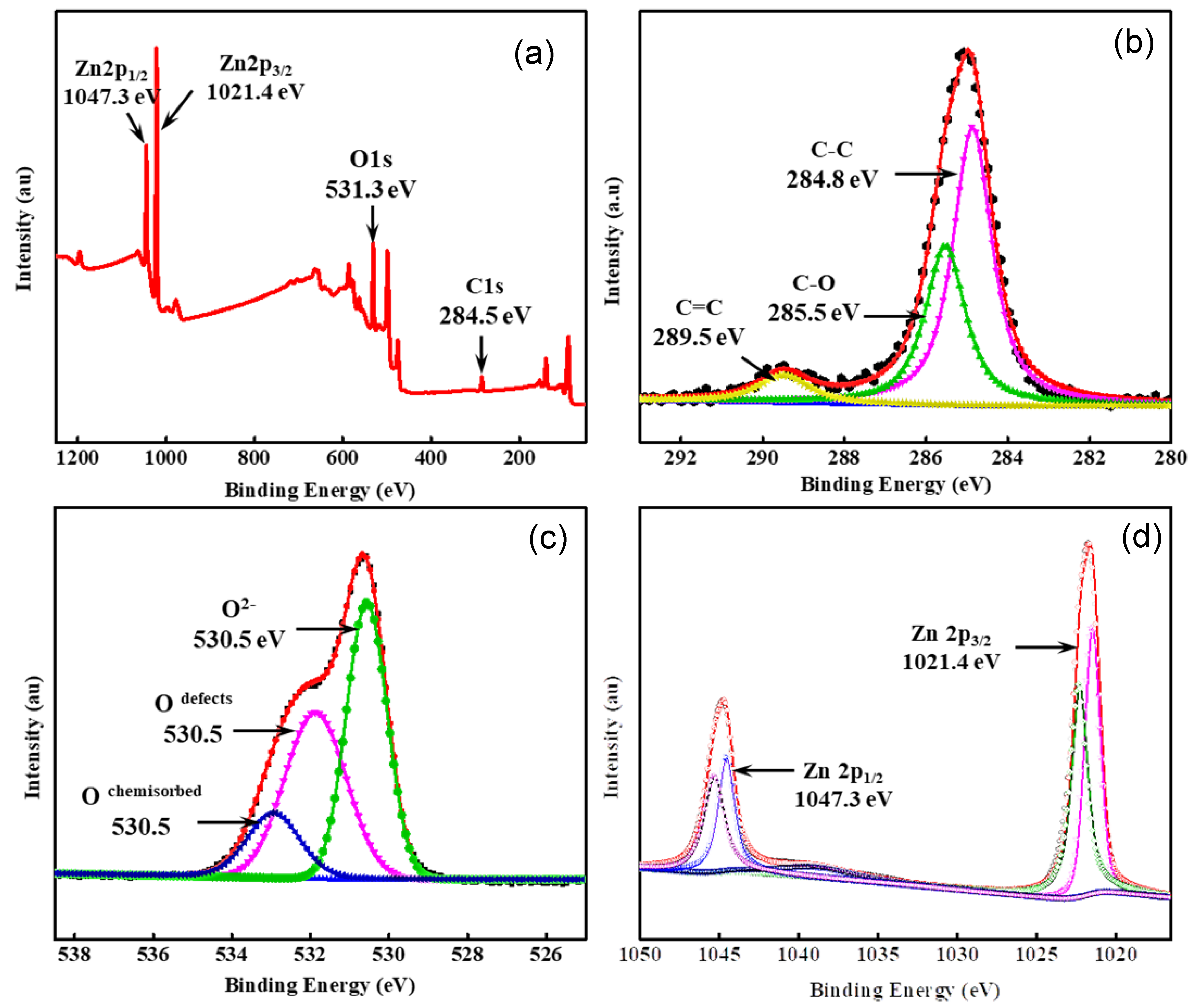
XPS analysis was performed to elucidate the elemental composition of ZnO/GO nanocomposite as well as the interfacial interaction among compositions (Figure 4). As shown in Figure 4a, the XPS survey spectra of ZnO/GO nanocomposites establish C1s, O1s, and Zn2p at 284.5 eV, 531.2 eV, and 1021.6–1047 eV, respectively. The deconvoluted peaks of the C1s spectrum at 284.8 eV, 285.5 eV, and 289.5 eV correspond to C-C, C-O, and C=C bonds, respectively, demonstrating that all contributed from GO [59]. The asymmetric O1s scan spectrum depicted in Figure 4d can be de-convoluted into three peaks where the binding energies are given to be 530.5 eV, 531.9 eV, and 533 eV, corresponding to the O2− in lattice (OL), O defects (OD), and O chemisorbed (OC), respectively [60]. Furthermore, the O2− ions, which are positioned on the ordinary lattice sites in the O1s spectrum, depict the possible contribution of the incorporated Zn ions. As shown in Figure 4d, the binding energy locations of 1021.4 eV and 1047.3 eV conform to the presence of two atomic states, Zn2p1/2 and Zn2p3/2, corresponding to the electronic state of Zn2+ [61]. These XPS data adequately confirm the successful accumulation of Zn within the GO lattice.
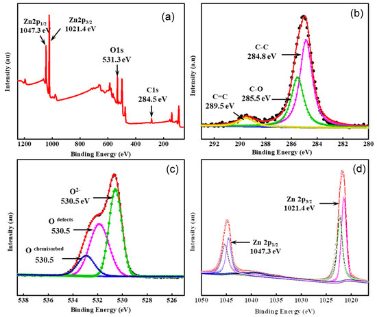
Figure 4.
XPS spectrum of (ZnO-3DG-0.25) showing (a) overall elements binding energies, (b) Zn scan, (c) C1s scan, and (d) O1s scan.
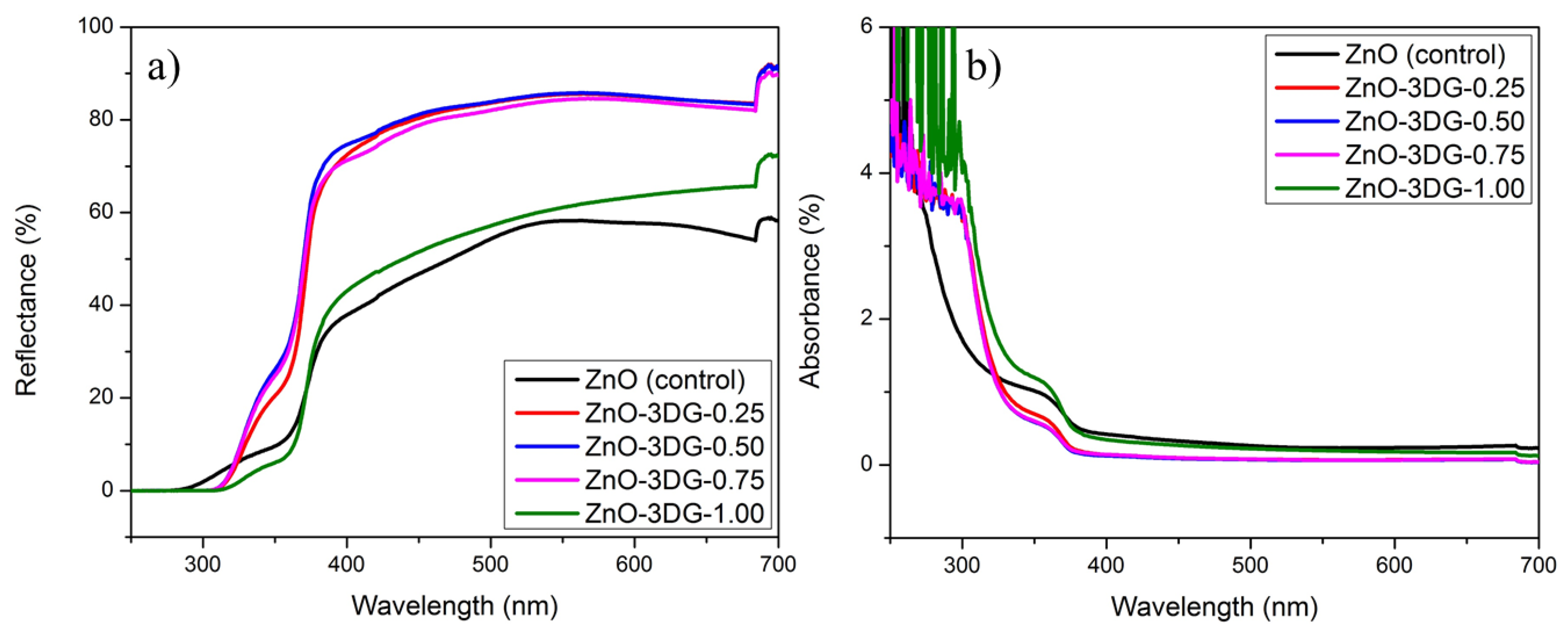
The UV-Vis spectrum for pristine and 3DG-modified ZnO thin films was analyzed to observe the reflectance and absorbance spectral responses. Figure 5 shows the reflectance and absorbance responses of pristine ZnO and ZnO-3DG-(0.25, 0.50, 0.75, and 1.00) ranging from 300 to 700 nm. The 3DG-modified ZnO with 0.25, 0.50, and 0.75 show higher reflectance across the 380 to 700 nm plateau at ≈80% compared to the ZnO-3DG-1.00 at ≈60%, while the pristine ZnO recorded at ≈55% is as shown in Figure 5a. Almost similar absorbance responses were recorded for all prepared samples across 380 to 700 nm. The decreased absorbance at ≈380 nm for ZnO-3DG-(0.25, 0.50, and 0.75) indicates less light absorption competition compared to the ZnO-3DG-1.00 and pristine ZnO.
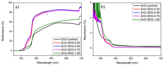
Figure 5.
UV-visible spectrum of ZnO control and ZnO-3DG-(0.25, 0.50, 0.75, and 1.00) showing the (a) reflectance and (b) absorbance.
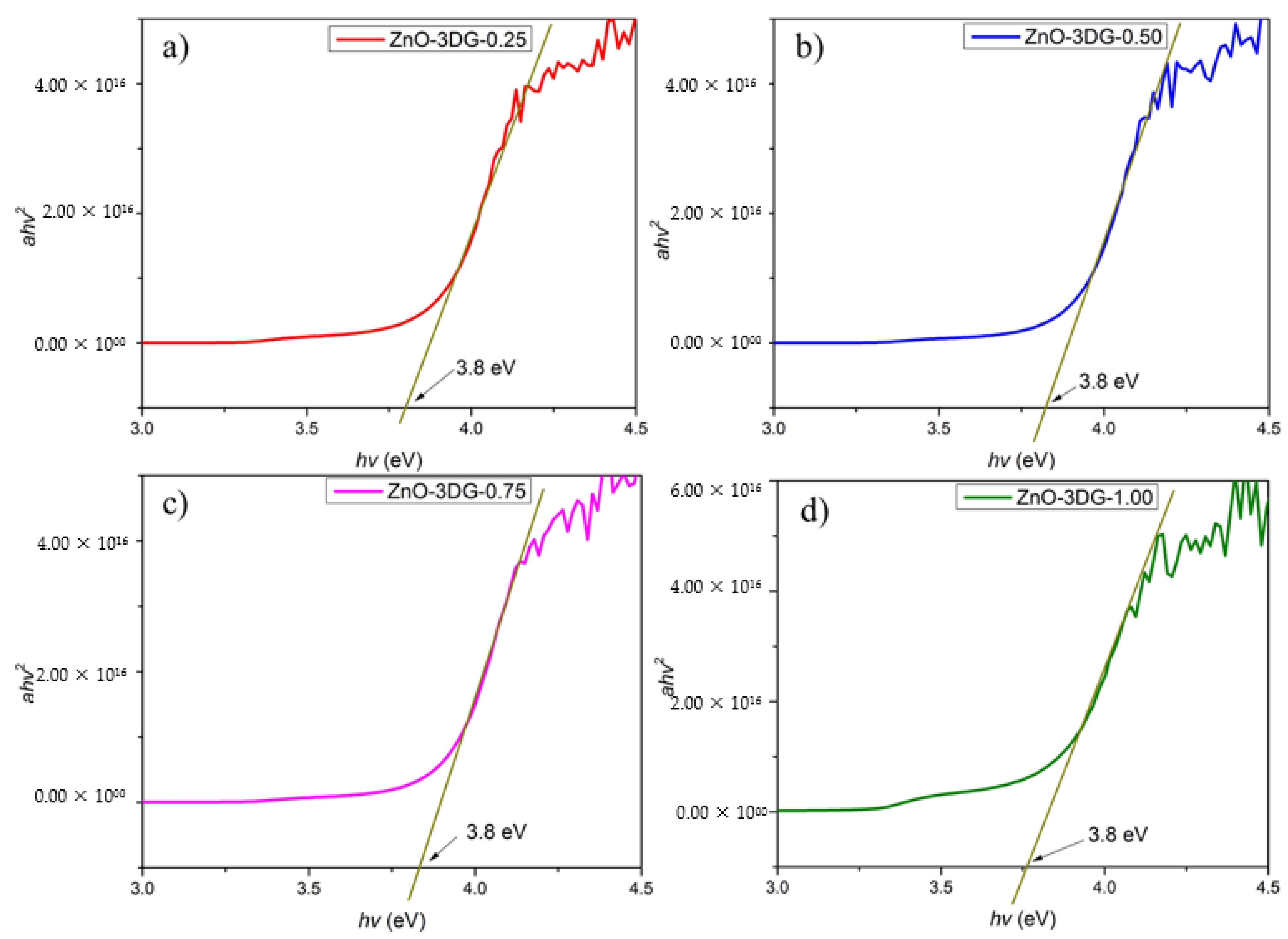
The band gap energies of pristine and 3D graphene-modified ZnO can be determined by formulating the Kubelka–Munk (K-M) equation. The analyzed data from the K-M equation can be plotted as a Tauc graph, and the interception of an extrapolated line at the x-axis determines the band gap energy. The absorbance coefficient can be obtained by the following formula, , where Eg is the energy band gap, A is the constant, v is the incident radiation frequency, and h is the Planck’s constant. Figure 6 shows the band gap energies obtained by hv versus (ahv)2, which indicates the absorbance coefficient. The obtained band gap for the 3DG-modified ZnO is 3.8 eV compared to the pristine ZnO at 3.23 eV. This enlarged band gap of ZnO-3DG is expected to result from the enhanced scattering of corresponding films as well as carbon doping within the ZnO photoanode. This band gap increment implies the decrease in particle size of ZnO-3DG, which is similar to the report by Zubair et al. [62].
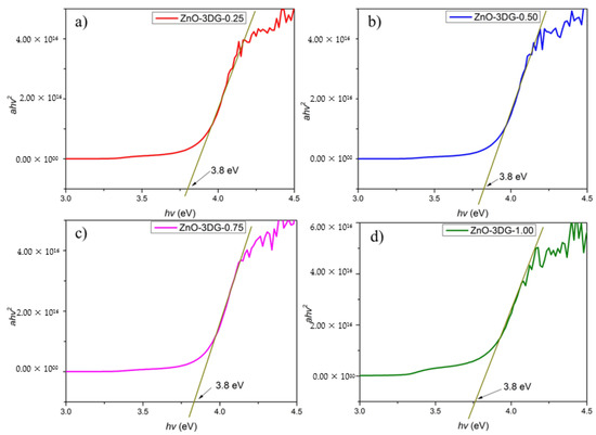
Figure 6.
Band gap energies for (a) ZnO-3DG-0.25, (b) ZnO-3DG-0.50, (c) ZnO-3DG-0.75, and (d) ZnO-3DG-1.00.
The modified photoanodes were used to fabricate perovskite solar cells. The perovskite is used as the light-absorbing material that was deposited by using the two-step sequential method, which is ideal for complete pore filling and production of the capping layer. It is observed in Figure 7 that the deposited perovskite on the ZnO-3DG layer successfully filled the pores.

Figure 7.
(a) FESEM cross-sectional image of CH3NH3PbI3 deposited on (a) ZnO and (b) (ZnO-3DG-0.25) thin films. Inset shows the respective surface morphology.
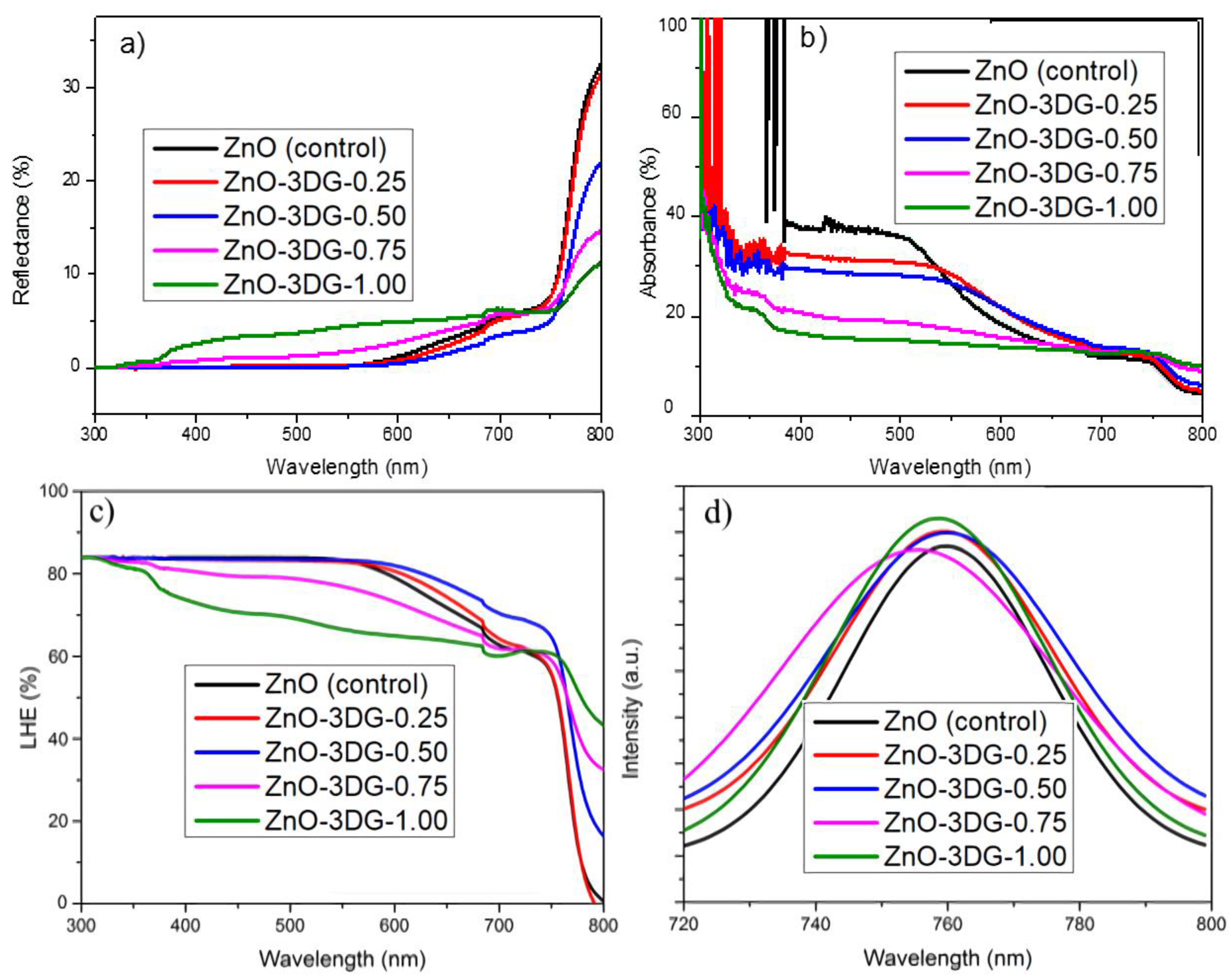
The optical properties of PSCs fabricated using ZnO-3DG were observed by absorbance, reflectance, and PL spectral responses. Figure 8a,b show the reflectance and absorbance spectrum ranging from 300 to 800 nm. The cell deposited with CH3NH3PbI3 shows superior absorbance at 760 nm, which is agreeable with the standard CH3NH3PbI3 absorbance. It also indicates the high quality of CH3NH3PbI3 obtained via the two-step sequential deposition [63]. As can be seen from Figure 8b, increasing the 3DG contents from 0.25 to 1.0 significantly decreases the absorbance. A device with a concentration of 0.25% 3DG shows the highest absorbance between the range 400 and 600 nm, which also reflects in the photovoltaics parameters. Similarly, Figure 8a shows an increase in reflectance with the increasing of the 3DG concentrations in the ZnO nanoparticles matrix. By evaluating the reflectance and absorbance data, the light-harvesting efficiency (LHE) for each fabricated PSC sample can be determined. The LHE can be calculated by using the equation, , where R and A are the reflectance and absorbance, respectively. Figure 8c shows the LHE for the control sample of ZnO and 3DG-modified ZnO thin films. The samples of ZnO-3DG-0.25 and 0.50 show higher efficiency of ≈82% at the visible region from 300 to 600 nm and gradually decrease from 600 to 800 nm compared to the control ZnO. The ZnO photoanodes with increased 3DG content of 0.75% and 1.00% show reduced LHE. The reduction in LHE is attributed to the competitive absorbance between the increased content of graphene and metal oxides. Steady-state PL was used to observe the photoanode quenching properties, which correlate to the electron transfer rate and the electron–hole recombination rate within the CH3NH3PbI3/ZnO-3DG interface. As illustrated in Figure 8d, the PL spectrum of the pristine ZnO shows lower quenching intensity for all the samples, indicating a slower charge recombination rate and faster electron transportation. Meanwhile, CH3NH3PbI3/ZnO-3DG-0.25 and 0.50 show PL quenching intensities that are closer to that of pristine ZnO, suggesting similar electron transfer and recombination behavior. As the 3DG content increased to 0.75% and 1.00%, the PL emission shows higher intensity and a shifted peak position, which implies a higher electron–hole recombination rate. These findings of PL quenching were further verified by the photocurrent density and photovoltage obtained for all the fabricated samples shown in Table 1.
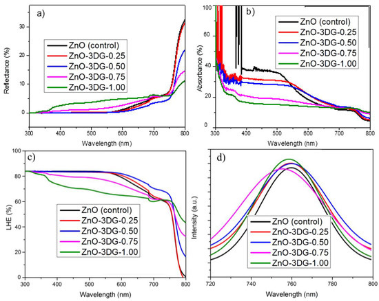
Figure 8.
(a) Reflectance, (b) absorbance, (c) LHE, and (d) steady-state PL of the ZnO-3DG-(025, 0.50, 0.75, and 1.00) coated with CH3NH3PbI3.

Table 1.
Photovoltaic parameters of PSCs using the pristine ZnO and ZnO-3DG ETMs.
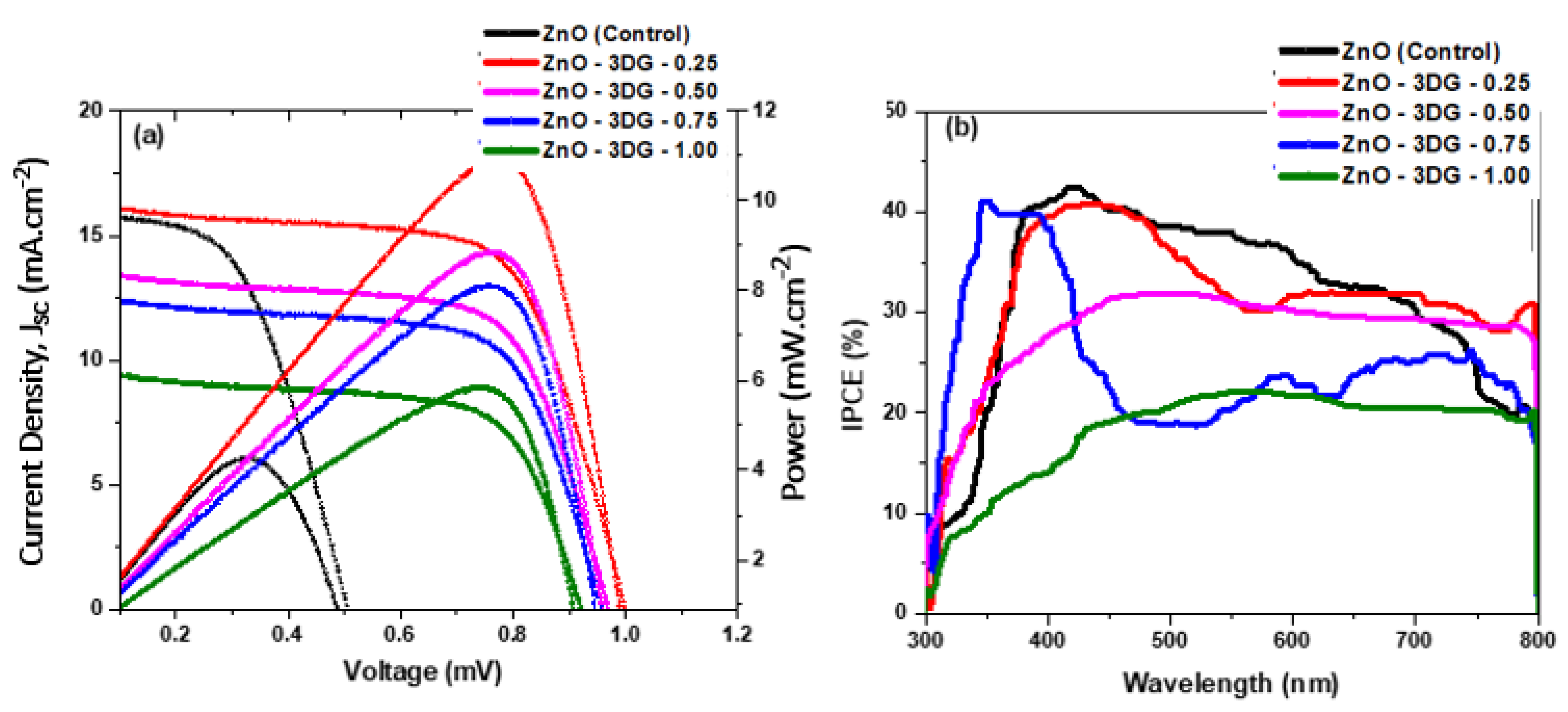
The measured photocurrent density–voltage (J-V) and IPCE for control ZnO and different 3DG samples are shown in Figure 9a,b, respectively. The JSC, VOC, FF, and the PCE of all the five cells are summarized in Table 1. The data show that all the photoanodes incorporated with 3DG recorded improvements in JSC and VOC compared to the control sample, although a systematic lowering was observed with the increase in concentration of 3DG. The highest PCE was delivered by ZnO-3DG-0.25 followed by 3DG modification of 0.5% and 0.75%. The ZnO-3DG-1.00 is able to deliver a PCE of 5.8%, which is higher compared with the control ZnO device (≈4.2%). From the plotted J-V graph as shown in Figure 9a, the ZnO-3DG-0.25-based device produced JSC ≈16.10 mA/cm2 and VOC ≈1.0 V, while ZnO-3DG-0.50 and 0.75 delivered 13.40 mA/cm2 and 12.40 mA/cm2, respectively. Despite the high JSC from control ZnO at 15.88 mA/cm2, the lower VOC reduced the PCE, whereas the 3DG-based devices exhibit high VOC. The ZnO-3DG-0.25 device showed only a nominally higher JSC compared to the control sample; however, the former registered 100% higher VOC and 25% higher FF than the ZnO-based control device. This phenomenon could be due to the better electron–hole separation, electron transportation, and reduced electron–hole recombination in the ZnO-3DG system. With better electron–hole separation, the enhancement in VOC can be observed in all the 3DG-modified photoanodes. However, with increased 3DG content, the JSC suffered due to increased recombination sites.
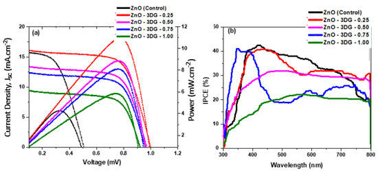
Figure 9.
(a) J-V curves and (b) IPCE of the control PSC and with different ZnO-3DG concentrations.
The electrochemical impedance was conducted to determine the interface resistance between the photoanode and the FTO as well as to determine the charge transport properties within the PSCs. In the Nyquist plot, the semicircle occurring at high frequency is attributed to the charge transfer resistance between the HTM and cathode, while the semicircle at low frequency is attributed to the charge transfer resistance between FTO and ZnO/perovskites [64]. On the other hand, the semicircle diameter size indicates the internal resistance of CH3NH3PbI3/ZnO-3DG [65,66]. As these PSCs are fabricated without the HTM, the secondary semicircle is not visible; hence, the charge transfer resistance is assigned to CH3NH3PbI3/3DG (cathode) [65]. Figure 10a shows the Nyquist plot for the control and 3DG-modified ZnO. The equivalent circuit for the PSCs is shown in Figure 10b, where RS represents the series resistance between FTO and ZnO/CH3NH3PbI3 and RCT is the charge transfer resistance in CH3NH3PbI3/3DG (cathode). From the Nyquist plot, the series resistance for ZnO-3DG-(0.25, 0.50, and 0.75) cells are almost diminished due to the low thickness of the ZnO film, which causes rapid charge transfer, whereas the ZnO-3DG-1.00 and the control ZnO RS can be seen, which implies a slower charge transfer. The size of semicircles followed the order of 0.25 > 0.50 > 0.75 > 1.00 > control ZnO, which indicates that the 3DG can reduce the internal resistance and improve the charge transport. However, as seen in the J-V and IPCE measurement, the JSC decreases as the 3DG content increases. This phenomenon suggests that during the light illumination, the excess 3DG structure started to competitively absorb light (photon) and become the recombination center rather than the electron distributor. In the cell with the low 3DG content, the graphene acts as the rapid electron transport material due to its high electron mobility. Table 2 summarizes the charge transport parameters RS, RCT, and constant phase element (CPE) The ZnO-3DG-0.25-based device showed the smallest RS followed by ZnO-3DG-0.75. Similarly, the device based on ZnO-3DG-0.25 shows the highest RCT value, as depicted in Table 2.
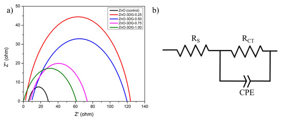
Figure 10.
Nyquist and fitted plots for (a) ZnO-control and ZnO-3DG-(0.25, 0.50, 0.75, and 1.00) (b) EIS equivalent circuit.

Table 2.
The charge transport parameters of the devices calculated from the EIS data.
4. Conclusions
In conclusion, the 3D graphene doped ZnO thin film has proven to be an electron transport layer that can contribute significantly to the photovoltage through efficient charge separation and transportation in addition to the significant improvement in the light-harvesting efficiency. This enhancement is not only displayed by PCE increment (10.9%) compared to the pristine ZnO (4.2%) but is also contributed by the two-fold photovoltage enhancement. The employed 3D graphene acts as the electron transporting ‘highway’ for the film with lower content 3D graphene and as an electron–hole recombination center for the film with higher content. A trade-off between higher 3D graphene and photocurrent density has been observed. It is observed that the dominant factor in the enhancement of light-harvesting efficiency is the connectivity and mobility of the carriers and the effective charge separation within the 3D framework of graphene rather than the generated current density. This development signifies that the new route for photovoltage enhancement can be employed in electron transport material to be utilized in photosynthesis devices.
Author Contributions
Conceptualization, M.S.M.S. (Mohamed Salleh Mohamed Saheed), N.M.M. and R.J.; methodology, M.S.M.S. (Mohamed Salleh Mohamed Saheed), B.S.M.S. and M.S.M.S. (Mohamed Shuaib Mohamed Saheed); software, M.S.M.S. (Mohamed Salleh Mohamed Saheed), Q.W., validation, M.S.M.S. (Mohamed Salleh Mohamed Saheed), B.S.M.S. and M.S.M.S. (Mohamed Shuaib Mohamed Saheed); formal analysis, M.S.M.S. (Mohamed Salleh Mohamed Saheed), B.S.M.S., M.S.M.S. (Mohamed Shuaib Mohamed Saheed), N.M.M., R.J. and Q.W.; investigation, M.S.M.S. (Mohamed Salleh Mohamed Saheed), B.S.M.S., M.S.M.S. (Mohamed Shuaib Mohamed Saheed), N.M.M. and R.J.; resources, N.M.M., R.J. and M.S.M.S. (Mohamed Shuaib Mohamed Saheed); writing—original draft preparation, M.S.M.S. (Mohamed Salleh Mohamed Saheed), M.S.M.S. (Mohamed Shuaib Mohamed Saheed) and R.J.; writing—review and editing, M.S.M.S. (Mohamed Salleh Mohamed Saheed), N.M.M., M.S.M.S. (Mohamed Shuaib Mohamed Saheed), R.J. and Q.W.; visualization, M.S.M.S. (Mohamed Salleh Mohamed Saheed) and Q.W.; supervision, N.M.M., M.S.M.S. (Mohamed Shuaib Mohamed Saheed) and R.J.; project administration, N.M.M., M.S.M.S. (Mohamed Shuaib Mohamed Saheed) and R.J.; funding acquisition, N.M.M., M.S.M.S. (Mohamed Shuaib Mohamed Saheed) and R.J. All authors have read and agreed to the published version of the manuscript.
Funding
Long Range Grant Scheme—Malaysia Institute for Innovative Nanotechnology (LRGS-NanoMITe: 0153AB-K50); RDU203301, Universiti Malaysia Pahang.
Institutional Review Board Statement
Not Applicable.
Informed Consent Statement
Not Applicable.
Data Availability Statement
All the data generated has been displayed in the paper.
Acknowledgments
This work is supported by Long Range Grant Scheme—Malaysia Institute for Innovative Nanotechnology (LRGS-NanoMITe: 0153AB-K50). RJ acknowledges the Research & Innovation Department of UMP (http://ump.edu.my, accessed on 1 December 2021) for RDU203301 aimed for perovskite solar cell research. The authors would also like to express their gratitude to Universiti Teknologi PETRONAS for the technical support.
Conflicts of Interest
The authors declare no competing financial interest.
References
- Kojima, A.; Teshima, K.; Shirai, Y.; Miyasaka, T. Organometal Halide Perovskites as Visible-Light Sensitizers for Photovoltaic Cells. J. Am. Chem. Soc. 2009, 131, 6050–6051. [Google Scholar] [CrossRef]
- Cai, Y.; Wen, J.; Liu, Z.; Qian, F.; Duan, C.; He, K.; Zhao, W.; Zhan, S.; Yang, S.; Cui, J.; et al. Graded 2D/3D (CF3-PEA)2FA0.85MA0.15Pb2I7/FA0.85MA0.15PbI3 heterojunction for stable perovskite solar cell with an efficiency over 23.0%. J. Energy Chem. 2022, 65, 480–489. [Google Scholar] [CrossRef]
- Liu, Y.; Gao, Y.; Lu, M.; Shi, Z.; Yu, W.W.; Hu, J.; Bai, X.; Zhang, Y. Ionic additive engineering for stable planar perovskite solar cells with efficiency >22%. Chem. Eng. J. 2021, 426, 130841. [Google Scholar] [CrossRef]
- Kim, J.Y.; Lee, J.W.; Jung, H.S.; Shin, H.; Park, N.G. High-Efficiency Perovskite Solar Cells. Chem. Rev. 2020, 120, 7867–7918. [Google Scholar] [CrossRef]
- Ling, J.; Kizhakkedath, P.K.K.; Watson, T.M.; Mora-Seró, I.; Schmidt-Mende, L.; Brown, T.M.; Jose, R. A Perspective on the Commercial Viability of Perovskite Solar Cells. Solar RRL 2021, 5, 2100401. [Google Scholar] [CrossRef]
- Fakharuddin, A.; Schmidt-Mende, L.; Garcia-Belmonte, G.; Jose, R.; Mora-Sero, I. Interfaces in Perovskite Solar Cells. Adv. Energy Mater. 2017, 7, 1700623. [Google Scholar] [CrossRef]
- Dong, Q.; Zhu, C.; Chen, M.; Jiang, C.; Guo, J.; Feng, Y.; Dai, Z.; Yadavalli, S.K.; Hu, M.; Cao, X.; et al. Interpenetrating interfaces for efficient perovskite solar cells with high operational stability and mechanical robustness. Nat. Commun. 2021, 12, 1–9. [Google Scholar] [CrossRef] [PubMed]
- Wali, Q.; Iqbal, Y.; Pal, B.; Lowe, A.; Jose, R. Tin oxide as an emerging electron transport medium in perovskite solar cells. Sol. Energy Mater. Sol. Cells 2018, 179, 102–117. [Google Scholar] [CrossRef]
- Consonni, V.; Briscoe, J.; Kärber, E.; Li, X.; Cossuet, T. ZnO nanowires for solar cells: A comprehensive review. Nanotechnology 2019, 30, 362001. [Google Scholar] [CrossRef] [PubMed]
- Lin, L.; Jones, T.W.; Yang, T.C.J.; Duffy, N.W.; Li, J.; Zhao, L.; Chi, B.; Wang, X.; Wilson, G.J. Inorganic Electron Transport Materials in Perovskite Solar Cells. Adv. Funct. Mater. 2021, 31, 2008300. [Google Scholar] [CrossRef]
- Wibowo, A.; Marsudi, M.A.; Amal, M.I.; Ananda, M.B.; Stephanie, R.; Ardy, H.; Diguna, L.J. ZnO nanostructured materials for emerging solar cell applications. RSC Adv. 2020, 10, 42838–42859. [Google Scholar] [CrossRef]
- Mahmud, M.A.; Elumalai, N.K.; Pal, B.; Jose, R.; Upama, M.B.; Wang, D.; Goncales, V.R.; Xu, C.; Haque, F.; Uddin, A. Electrospun 3D composite nano-flowers for high performance triple-cation perovskite solar cells. Electrochim. Acta 2018, 289, 459–473. [Google Scholar] [CrossRef]
- Dai, X.; Koshy, P.; Sorrell, C.C.; Lim, J.; Yun, J.S. Focussed Review of Utilization of Graphene-Based Materials in Electron Transport Layer in Halide Perovskite Solar Cells: Materials-Based Issues. Energies 2020, 13, 6335. [Google Scholar] [CrossRef]
- Gatti, T.; Menna, E.; Meneghetti, M.; Maggini, M.; Petrozza, A.; Lamberti, F. The Renaissance of fullerenes with perovskite solar cells. Nano Energy 2017, 41, 84–100. [Google Scholar] [CrossRef]
- Iqbal, M.Z.; Rehman, A.-U. Recent progress in graphene incorporated solar cell devices. Sol. Energy 2018, 169, 634–647. [Google Scholar] [CrossRef]
- Fakharuddin, A.; Di Giacomo, F.; Ahmed, I.; Wali, Q.; Brown, T.M.; Jose, R. Role of morphology and crystallinity of nanorod and planar electron transport layers on the performance and long term durability of perovskite solar cells. J. Power Sources 2015, 283, 61–67. [Google Scholar] [CrossRef] [Green Version]
- Maniarasu, S.; Karthikeyan, V.; Korukonda, T.B.; Pradhan, S.C.; Soman, S.; Ramasamy, E.; Veerappan, G. Ambient processed perovskite sensitized porous TiO2 nanorods for highly efficient and stable perovskite solar cells. J. Alloy. Compd. 2021, 884, 161061. [Google Scholar] [CrossRef]
- Elseman, A.M.; Zaki, A.H.; Shalan, A.E.; Rashad, M.M.; Song, Q.L. TiO2 Nanotubes: An Advanced Electron Transport Material for Enhancing the Efficiency and Stability of Perovskite Solar Cells. Ind. Eng. Chem. Res. 2020, 59, 18549–18557. [Google Scholar] [CrossRef]
- Mohammed, M.K. 21.4% efficiency of perovskite solar cells using BMImI additive in the lead iodide precursor based on carbon nanotubes/TiO2 electron transfer layer. Ceram. Int. 2020, 46, 27647–27654. [Google Scholar] [CrossRef]
- Nwankwo, U.; Ngqoloda, S.; Nkele, A.C.; Arendse, C.J.; Ozoemena, K.I.; Ekwealor, A.B.C.; Jose, R.; Maaza, M.; Ezema, F.I. Effects of alkali and transition metal-doped TiO2 hole blocking layers on the perovskite solar cells obtained by a two-step sequential deposition method in air and under vacuum. RSC Adv. 2020, 10, 13139–13148. [Google Scholar] [CrossRef] [Green Version]
- Yin, Z.; Zhu, J.; He, Q.; Cao, X.; Tan, C.; Chen, H.; Yan, Q.; Zhang, H. Graphene-Based Materials for Solar Cell Applications. Adv. Energy Mater. 2014, 4, 1300574. [Google Scholar] [CrossRef]
- Agresti, A.; Pescetelli, S.; Taheri, B.; Del Rio Castillo, A.E.; Cinà, L.; Bonaccorso, F.; Di Carlo, A. Graphene-Perovskite Solar Cells Exceed 18% Efficiency: A Stability Study. ChemSusChem 2016, 9, 2609–2619. [Google Scholar] [CrossRef] [PubMed]
- Chandiran, A.K.; Abdi-Jalebi, M.; Nazeeruddin, M.K.; Grätzel, M. Analysis of Electron Transfer Properties of ZnO and TiO2 Photoanodes for Dye-Sensitized Solar Cells. ACS Nano 2014, 8, 2261–2268. [Google Scholar] [CrossRef]
- Si, H.; Kang, Z.; Liao, Q.; Zhang, Z.; Zhang, X.; Wang, L.; Zhang, Y. Design and tailoring of patterned ZnO nanostructures for energy conversion applications. Sci. China Mater. 2017, 60, 793–810. [Google Scholar] [CrossRef]
- Saheed, M.S.M.; Mohamed, N.M.; Singh, B.S.M.; Jose, R. Surface Plasmon Assisted Electron–Hole Migration for High Photocurrent Density Generation in a Perovskite Solar Cell. ACS Appl. Energy Mater. 2019, 2, 8707–8714. [Google Scholar] [CrossRef]
- Bakr, Z.H.; Wali, Q.; Ismail, J.; Elumalai, N.K.; Uddin, A.; Jose, R. Synergistic combination of electronic and electrical properties of SnO2 and TiO2 in a single SnO2-TiO2 composite nanofiber for dye-sensitized solar cells. Electrochim. Acta 2018, 263, 524–532. [Google Scholar] [CrossRef]
- Cao, J.; Wu, B.; Chen, R.; Wu, Y.; Hui, Y.; Mao, B.-W.; Zheng, N. Efficient, Hysteresis-Free, and Stable Perovskite Solar Cells with ZnO as Electron-Transport Layer: Effect of Surface Passivation. Adv. Mater. 2018, 30, 1705596. [Google Scholar] [CrossRef]
- Jose, R.; Thavasi, V.; Ramakrishna, S. Metal Oxides for Dye-Sensitized Solar Cells. J. Am. Ceram. Soc. 2009, 92, 289–301. [Google Scholar] [CrossRef]
- Ning, R.; Takeuchi, M.; Lin, J.-M.; Saito, T.; Isogai, A. Influence of the morphology of zinc oxide nanoparticles on the properties of zinc oxide/nanocellulose composite films. React. Funct. Polym. 2018, 131, 293–298. [Google Scholar] [CrossRef]
- Shi, Z.; Li, Y.; Li, S.; Li, X.; Wu, D.; Xu, T.; Tian, Y.; Chen, Y.; Zhang, Y.; Zhang, B.; et al. Localized Surface Plasmon Enhanced All-Inorganic Perovskite Quantum Dot Light-Emitting Diodes Based on Coaxial Core/Shell Heterojunction Architecture. Adv. Funct. Mater. 2018, 28, 1707031. [Google Scholar] [CrossRef]
- Sun, Y.; Gao, Y.; Hu, J.; Liu, C.; Sui, Y.; Lv, S.; Wang, F.; Yang, L. Comparison of effects of ZnO and TiO2 compact layer on performance of perovskite solar cells. J. Solid State Chem. 2020, 287, 121387. [Google Scholar] [CrossRef]
- Mahadik, S.A.; Patil, A.; Pathan, H.M.; Salunke-Gawali, S.; Butcher, R.J. Thionaphthoquinones as Photosensitizers for TiO2 Nanorods and ZnO Nanograin Based Dye-sensitized Solar Cells: Effect of Nanostructures on Charge Transport and Photovoltaic Performance. Eng. Sci. 2020, 14, 46–58. [Google Scholar] [CrossRef]
- Nemiwal, M.; Zhang, T.C.; Kumar, D. Recent progress in g-C3N4, TiO2 and ZnO based photocatalysts for dye degradation: Strategies to improve photocatalytic activity. Sci. Total Environ. 2021, 767, 144896. [Google Scholar] [CrossRef]
- Bagha, G.; Mersagh, M.R.; Naffakh-Moosavy, H.; Matin, L.F. The role of rGO sheet and Ag dopant in reducing ZnO electron transport layer recombination in planar perovskite solar cells. Ceram. Int. 2021, 47, 16111–16123. [Google Scholar] [CrossRef]
- Bagha, G.; Naffakh-Moosavy, H.; Mersagh, M.R. The effect of reduced graphene oxide sheet on the optical and electrical characteristics of Ni-doped and Ag-doped ZnO ETLs in planar perovskite solar cells. J. Alloy. Compd. 2021, 870, 159658. [Google Scholar] [CrossRef]
- Chen, C.J.; Chandel, A.; Thakur, D.; Wu, J.R.; Chiang, S.E.; Zeng, G.S.; Shen, J.L.; Chen, S.H.; Chang, S.H. Ag modified bathocuproine:ZnO nanoparticles electron buffer layer based bifacial inverted-type perovskite solar cells. Org. Electron. 2021, 92, 106110. [Google Scholar] [CrossRef]
- Kang, J.; Han, K.; Sun, X.; Zhang, L.; Huang, R.; Ismail, I.; Wang, Z.; Ding, C.; Zha, W.; Li, F.; et al. Suppression of Ag migration by low-temperature sol-gel zinc oxide in the Ag nanowires transparent electrode-based flexible perovskite solar cells. Org. Electron. 2020, 82, 105714. [Google Scholar] [CrossRef]
- Liu, M.; Chen, Z.; Yang, Y.; Yip, H.-L.; Cao, Y. Reduced open-circuit voltage loss for highly efficient low-bandgap perovskite solar cells via suppression of silver diffusion. J. Mater. Chem. A 2019, 7, 17324–17333. [Google Scholar] [CrossRef]
- Azri, F.; Meftah, A.; Sengouga, N.; Meftah, A. Electron and hole transport layers optimization by numerical simulation of a perovskite solar cell. Sol. Energy 2019, 181, 372–378. [Google Scholar] [CrossRef]
- Irandoost, R.; Soleimani-Amiri, S. Design and analysis of high efficiency perovskite solar cell with ZnO nanorods and plasmonic nanoparticles. Optik 2020, 202, 163598. [Google Scholar] [CrossRef]
- Tulus; Olthof, S.; Marszalek, M.; Peukert, A.; Muscarella, L.A.; Ehrler, B.; Vukovic, O.; Galagan, Y.; Boehme, S.C.; Von Hauff, E. Control of Surface Defects in ZnO Nanorod Arrays with Thermally Deposited Au Nanoparticles for Perovskite Photovoltaics. ACS Appl. Energy Mater. 2019, 2, 3736–3748. [Google Scholar] [CrossRef] [Green Version]
- Alshehri, A.H.; Loke, J.Y.; Nguyen, V.H.; Jones, A.; Asgarimoghaddam, H.; Delumeau, L.V.; Shahin, A.; Ibrahim, K.H.; Mistry, K.; Yavuz, M.; et al. Nanoscale Film Thickness Gradients Printed in Open Air by Spatially Varying Chemical Vapor Deposition. Adv. Funct. Mater. 2021, 31, 2103271. [Google Scholar] [CrossRef]
- Liu, X.; Iocozzia, J.; Wang, Y.; Cui, X.; Chen, Y.; Zhao, S.; Li, Z.; Lin, Z. Noble metal–metal oxide nanohybrids with tailored nanostructures for efficient solar energy conversion, photocatalysis and environmental remediation. Energy Environ. Sci. 2017, 10, 402–434. [Google Scholar] [CrossRef]
- Bi, D.; Boschloo, G.; Schwarzmüller, S.; Yang, L.; Johansson, E.M.J.; Hagfeldt, A. Efficient and stable CH3NH3PbI3-sensitized ZnO nanorod array solid-state solar cells. Nanoscale 2013, 5, 11686–11691. [Google Scholar] [CrossRef] [PubMed] [Green Version]
- Chen, P.; Yin, X.; Que, M.; Yang, Y.; Que, W. TiO2 passivation for improved efficiency and stability of ZnO nanorods based perovskite solar cells. RSC Adv. 2016, 6, 57996–58002. [Google Scholar] [CrossRef]
- Liang, Y.-C.; Hu, C.-Y.; Zhong, H. Effects of ultrathin layers on the growth of vertically aligned wurtzite ZnO nanostructures on perovskite single-crystal substrates. Appl. Surf. Sci. 2012, 261, 633–639. [Google Scholar] [CrossRef]
- Chandrasekhar, P.; Dubey, A.; Qiao, Q. High efficiency perovskite solar cells using nitrogen-doped graphene/ZnO nanorod composite as an electron transport layer. Sol. Energy 2020, 197, 78–83. [Google Scholar] [CrossRef]
- Chandrasekhar, P.S.; Komarala, V.K. Graphene/ZnO nanocomposite as an electron transport layer for perovskite solar cells; the effect of graphene concentration on photovoltaic performance. RSC Adv. 2017, 7, 28610–28615. [Google Scholar] [CrossRef] [Green Version]
- Tavakoli, M.M.; Tavakoli, R.; Nourbakhsh, Z.; Waleed, A.; Virk, U.S.; Fan, Z. High Efficiency and Stable Perovskite Solar Cell Using ZnO/rGO QDs as an Electron Transfer Layer. Adv. Mater. Interfaces 2016, 3, 1500790. [Google Scholar] [CrossRef]
- Tavakoli, M.M.; Tavakoli, R.; Yadav, P.; Kong, J. A graphene/ZnO electron transfer layer together with perovskite passivation enables highly efficient and stable perovskite solar cells. J. Mater. Chem. A 2019, 7, 679–686. [Google Scholar] [CrossRef] [Green Version]
- Krishnan, S.G.; Harilal, M.; Yar, A.; Vijayan, B.L.; Dennis, J.O.; Yusoff, M.; Jose, R. Critical influence of reduced graphene oxide mediated binding of M (M = Mg, Mn) with Co ions, chemical stability and charge storability enhancements of spinal-type hierarchical MCo2O4 nanostructures. Electrochim. Acta 2017, 243, 119–128. [Google Scholar] [CrossRef]
- Hu, H.; Zhao, Z.; Wan, W.; Gogotsi, Y.; Qiu, J. Ultralight and Highly Compressible Graphene Aerogels. Adv. Mater. 2013, 25, 2219–2223. [Google Scholar] [CrossRef] [PubMed]
- Jo, S.B.; Lee, J.H.; Sim, M.; Kim, M.; Park, J.H.; Choi, Y.S.; Kim, Y.; Ihn, S.-G.; Cho, K. High Performance Organic Photovoltaic Cells Using Polymer-Hybridized ZnO Nanocrystals as a Cathode Interlayer. Adv. Energy Mater. 2011, 1, 690–698. [Google Scholar] [CrossRef]
- Perumal, V.; Hashim, U.; Gopinath, S.C.; Haarindraprasad, R.; Foo, K.; Balakrishnan, S.R.; Poopalan, P. ‘Spotted Nanoflowers’: Gold-seeded Zinc Oxide Nanohybrid for Selective Bio-capture. Sci. Rep. 2015, 5, 12231. [Google Scholar] [CrossRef] [Green Version]
- Saheed, M.S.M.; Mohamed, N.M.; Singh, B.S.M. Precursor and pressure dependent 3D graphene: A study on layer formation and type of carbon material. Diam. Relat. Mater. 2017, 79, 93–101. [Google Scholar] [CrossRef]
- Ong, C.C.; Jose, R.; Saheed, M.S.M. Phase transformed iron oxide-iron (oxy) hydroxide composite nanoflorets grown on foam-like graphene as a high performing adsorbent. Chem. Eng. J. 2020, 388, 124306. [Google Scholar] [CrossRef]
- Burschka, J.; Pellet, N.; Moon, S.-J.; Humphry-Baker, R.; Gao, P.; Nazeeruddin, M.K.; Grätzel, M. Sequential deposition as a route to high-performance perovskite-sensitized solar cells. Nat. Cell Biol. 2013, 499, 316–319. [Google Scholar] [CrossRef]
- Shao, S.; Loi, M.A. The Role of the Interfaces in Perovskite Solar Cells. Adv. Mater. Interfaces 2019, 7, 1901469. [Google Scholar] [CrossRef] [Green Version]
- Akhtar, M.H.; Mir, T.A.; Gurudatt, N.; Chung, S.; Shim, Y.-B. Sensitive NADH detection in a tumorigenic cell line using a nano-biosensor based on the organic complex formation. Biosens. Bioelectron. 2016, 85, 488–495. [Google Scholar] [CrossRef]
- Haldorai, Y.; Voit, W.; Shim, J.J. Nano ZnO@reduced graphene oxide composite for high performance supercapacitor: Green synthesis in supercritical fluid. Electrochim. Acta 2014, 120, 65–72. [Google Scholar] [CrossRef]
- Pal, S.; Gogurla, N.; Das, A.; Singha, S.S.; Kumar, P.; Kanjilal, D.K.; Singha, A.; Chattopadhyay, S.; Jana, D.; Sarkar, A. Clustered vacancies in ZnO: Chemical aspects and consequences on physical properties. J. Phys. D Appl. Phys. 2018, 51, 105107. [Google Scholar] [CrossRef] [Green Version]
- Zubair, M.; Mustafa, M.; Ali, A.; Doh, Y.H.; Choi, K.H. Improvement of solution based conjugate polymer organic light emitting diode by ZnO–graphene quantum dots. J. Mater. Sci. Mater. Electron. 2015, 26, 3344–3351. [Google Scholar] [CrossRef]
- Iftikhar, F.J.; Wali, Q.; Yang, S.; Iqbal, Y.; Jose, R.; Munir, S.; Gondal, I.A.; Khan, M.E. Structural and optoelectronic properties of hybrid halide perovskites for solar cells. Org. Electron. 2021, 91, 106077. [Google Scholar] [CrossRef]
- Figueiredo-Filho, L.C.S.; Brownson, D.A.C.; Fatibello-Filho, O.; Banks, C.E. Electroanalytical Performance of a Freestanding Three-Dimensional Graphene Foam Electrode. Electroanalysis 2014, 26, 93–102. [Google Scholar] [CrossRef]
- Chen, H.; Wei, Z.; He, H.; Zheng, X.; Wong, K.S.; Yang, S. Solvent Engineering Boosts the Efficiency of Paintable Carbon-Based Perovskite Solar Cells to Beyond 14%. Adv. Energy Mater. 2016, 6, 1502087. [Google Scholar] [CrossRef]
- Wang, B.X.; Liu, T.F.; Zhou, Y.B.; Chen, X.; Yuan, X.B.; Yang, Y.Y.; Liu, W.P.; Wang, J.M.; Han, H.W.; Tang, Y.W. Hole-conductor-free perovskite solar cells with carbon counter electrodes based on ZnO nanorod arrays. Phys. Chem. Chem. Phys. 2016, 18, 27078–27082. [Google Scholar] [CrossRef] [PubMed]
Publisher’s Note: MDPI stays neutral with regard to jurisdictional claims in published maps and institutional affiliations. |
© 2021 by the authors. Licensee MDPI, Basel, Switzerland. This article is an open access article distributed under the terms and conditions of the Creative Commons Attribution (CC BY) license (https://creativecommons.org/licenses/by/4.0/).


