Article

A CMOS-Based Power Management Circuit with a Reconfigurable Rectifier and an LDO Regulator for Piezoelectric Energy Harvesting in IoT Applications

by
Suany E. Vázquez-Valdés
1,
Primavera Argüelles-Lucho
2,3,
Rosa M. Woo-García
1,2,
Edith Osorio-de-la-Rosa
4,
Francisco López-Huerta
2,* and
Agustín L. Herrera-May
1,5,*
1
Faculty of Construction and Habitat Engineering, Universidad Veracruzana, Boca del Río 94294, Veracruz, Mexico
2
Faculty of Electrical and Electronic Engineering, Universidad Veracruzana, Boca del Río 94294, Veracruz, Mexico
3
National Technology of Mexico, Veracruz Technological Institute, Veracruz 91800, Veracruz, Mexico
4
Secretariat of Science, Humanities, Technology and Innovation (SECIHTI), Autonomous University of the State of Quintana Roo, Chetumal 77019, Quintana Roo, Mexico
5
Micro and Nanotechnology Research Center, Universidad Veracruzana, Boca del Río 94294, Veracruz, Mexico
*
Authors to whom correspondence should be addressed.
Nanoenergy Adv. 2025, 5(2), 7; https://doi.org/10.3390/nanoenergyadv5020007
Submission received: 4 February 2025 / Revised: 18 April 2025 / Accepted: 8 May 2025 / Published: 14 May 2025

Abstract

:
The technological advances in internet of things (IoT) devices have raised the demand for cost-efficient and sustainable energy sources. Piezoelectric energy harvesters (PEHs) are promising low-cost and eco-friendly energy sources but require robust power management circuits (PMCs) for voltage conversion and regulation. This work presents a complementary metal–oxide–semiconductor (CMOS)-based PMC, integrating a reconfigurable AC-DC rectifier and a low-dropout (LDO) voltage regulator designed using 0.18 µm Taiwan semiconductor manufacturing company (TSMC) CMOS technology. This design includes an intermediate coupling stage to reduce voltage drop and improve the transfer efficiency of the PMC. In addition, we develop numerical simulations of the PMC performance, achieving a voltage conversion efficiency (VCE) between 72.8% and 43.21% using input voltages from 0.7 V to 2.8 V with a 50 kΩ load resistance. Compared to previous designs, the proposed circuit demonstrates improved stability, reduced area (66.28 mm2), and extended operating voltage range, allowing its potential application for ultra-low-power IoT nodes. This PMC contributes to the development of autonomous systems with reduced battery dependency and enhanced sustainability.

1. Introduction

The rapid expansion of internet of things (IoT) technologies in fields such as healthcare, environmental monitoring, and smart infrastructure has created a pressing need for miniaturized, autonomous, and energy-efficient electronic systems [1,2]. Wearable and implantable IoT devices demand long-term energy autonomy to reduce maintenance cycles, eliminate battery replacements, and support continuous operation in constrained environments [3]. Piezoelectric energy harvesters (PEHs) can convert mechanical vibrations or stress into electrical energy. These PEHs represent a sustainable solution for powering low-power systems due to their compact size, low environmental impact, and capacity for continuous energy generation [4,5,6]. These mechanisms, along with other ambient energy harvesting techniques such as triboelectric, thermoelectric, and electromagnetic conversion, have gained relevance in recent years [7]. Nonetheless, energy generated by PEHs is typically alternating current (AC), which must be rectified and regulated to produce usable direct current (DC) voltage for digital electronics [8]. To achieve this, power management circuits (PMCs) are employed to perform AC-DC conversion and supply regulation [9].
Generally, PMCs consist of rectifier topologies followed by DC-DC converters or linear regulators such as low-dropout regulators (LDOs), each with distinct trade-offs in terms of voltage conversion efficiency (VCE), power conversion efficiency (PCE), response time, and silicon area [10,11]. For example, LDOs provide low noise and fast response, but their efficiency may decrease significantly when the voltage difference between the input and output is large [12]. Recent studies have investigated switched-capacitor (SC) DC-DC converters [13], supercapacitor integration [14], and impedance adaptation for improved energy matching [15,16]. Although many of these solutions demonstrate efficiency under specific conditions, they often struggle to maintain performance across broad voltage ranges or introduce significant area overheads [17,18,19]. Additionally, research has focused on minimizing losses and increasing stability by introducing adaptive rectification, dynamic biasing, and hybrid configurations that combine LDOs with charge pump or switched-capacitor elements [20,21]. Such innovations are critical to supporting IoT applications that require consistent voltage levels under fluctuating energy inputs. Although previous research has proposed energy harvesting circuits for low-power applications [22,23], several works are constrained by narrow operating voltage ranges, a large footprint, or instability under dynamic loading. Consequently, there remains a significant need for PMCs that ensure reliable energy conditioning under highly variable transducer outputs, with minimal design complexity and power loss. This research direction is aligned with current technological trends toward sustainable smart environments and wearable health monitoring platforms, which demand robust energy management strategies tailored to intermittently powered conditions [24,25].
Herein, we propose a complementary metal–oxide–semiconductor (CMOS)-based PMC specifically optimized for piezoelectric energy harvesting. The design integrates the following three functional blocks: (1) a reconfigurable AC-DC rectifier, (2) a coupling stage based on transmission gates and a coupling capacitor, and (3) a low-dropout voltage regulator. The novelty of this work lies in its architecture that enables reduced dropout voltage, extended input ranges from 0.7 V to 2.8 V, and improved energy transfer efficiency compared to previously reported designs [26]. The reconfigurable nature of the rectifier allows dynamic adaptation to varying input levels, while the coupling stage minimizes inter-stage losses, enhancing the overall voltage conversion process [27]. This research makes the following contributions to the field of energy harvesting for IoT devices:
(i)
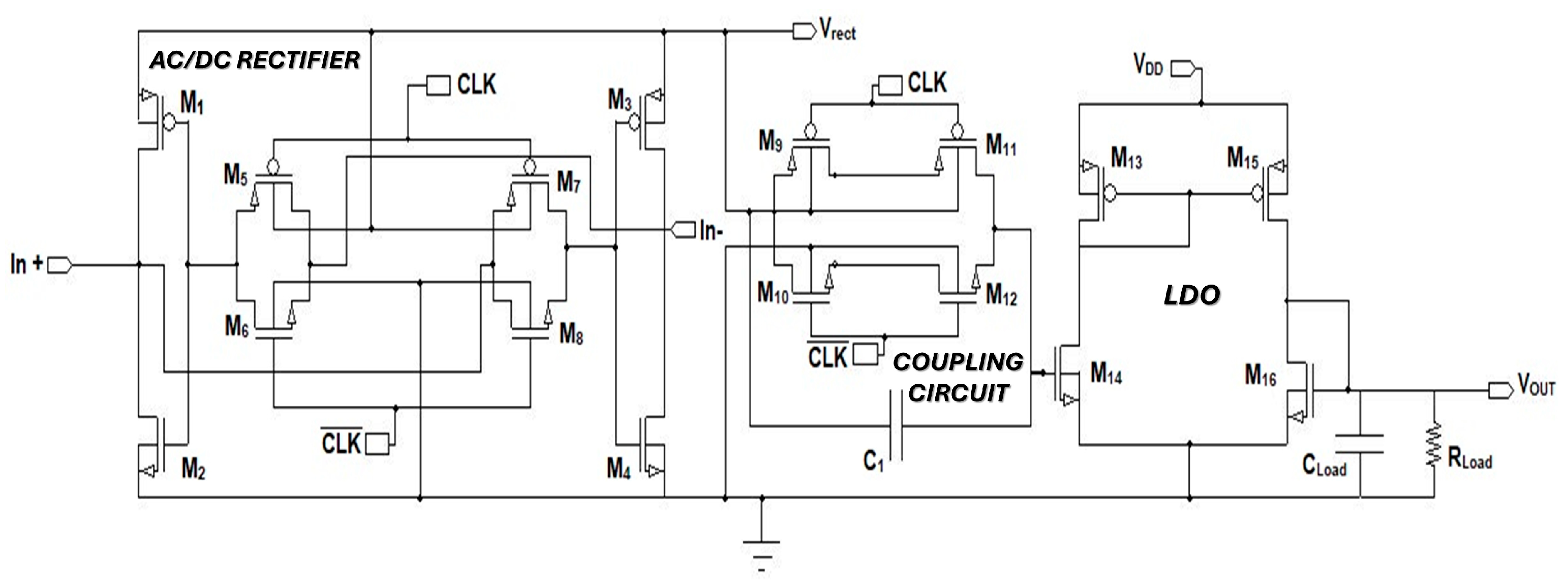
Introduces a novel reconfigurable rectifier–coupling–regulator architecture fabricated in 0.18 µm from Taiwan semiconductor manufacturing company (TSMC) for piezoelectric harvester CMOS technology.
(ii)
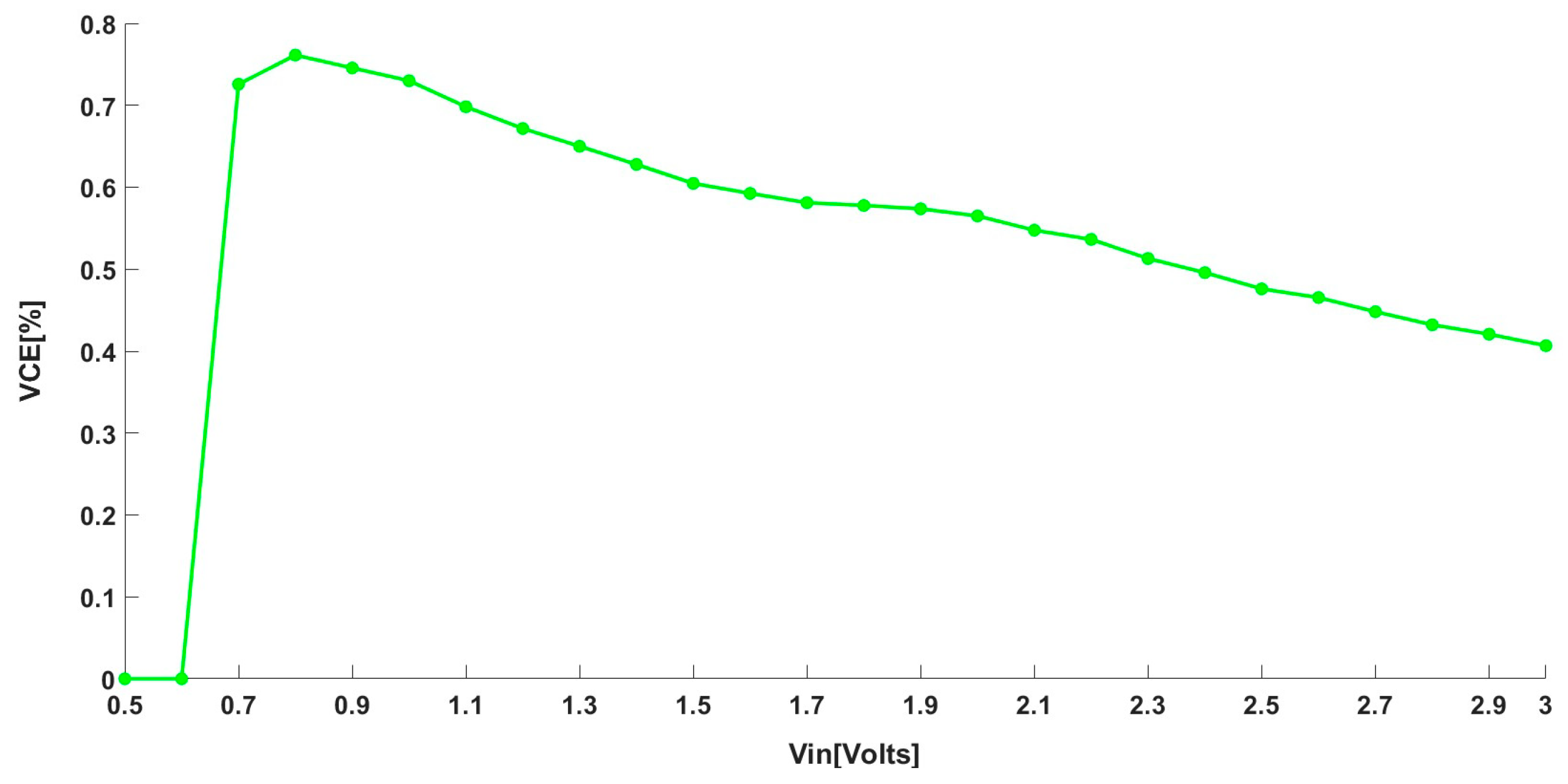
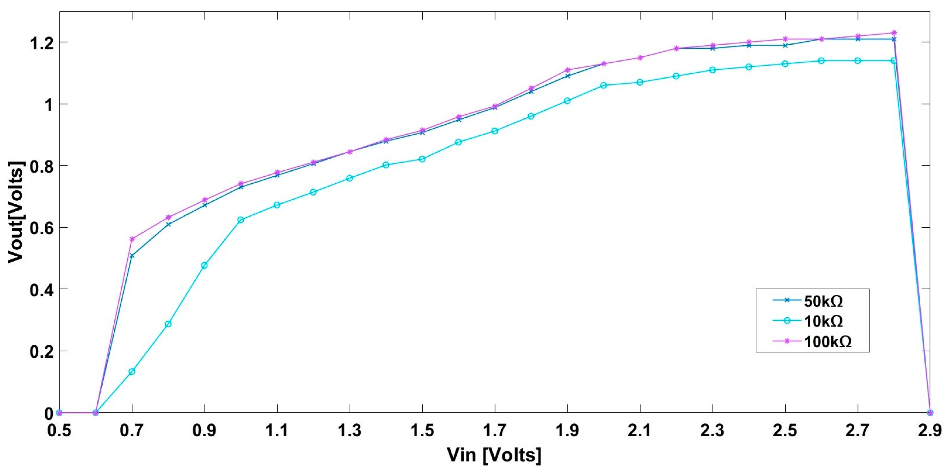
Achieves wide-range input operation from 0.7 V to 2.8 V, maintaining high VCE (72.8% to 43.21%).
(iii)
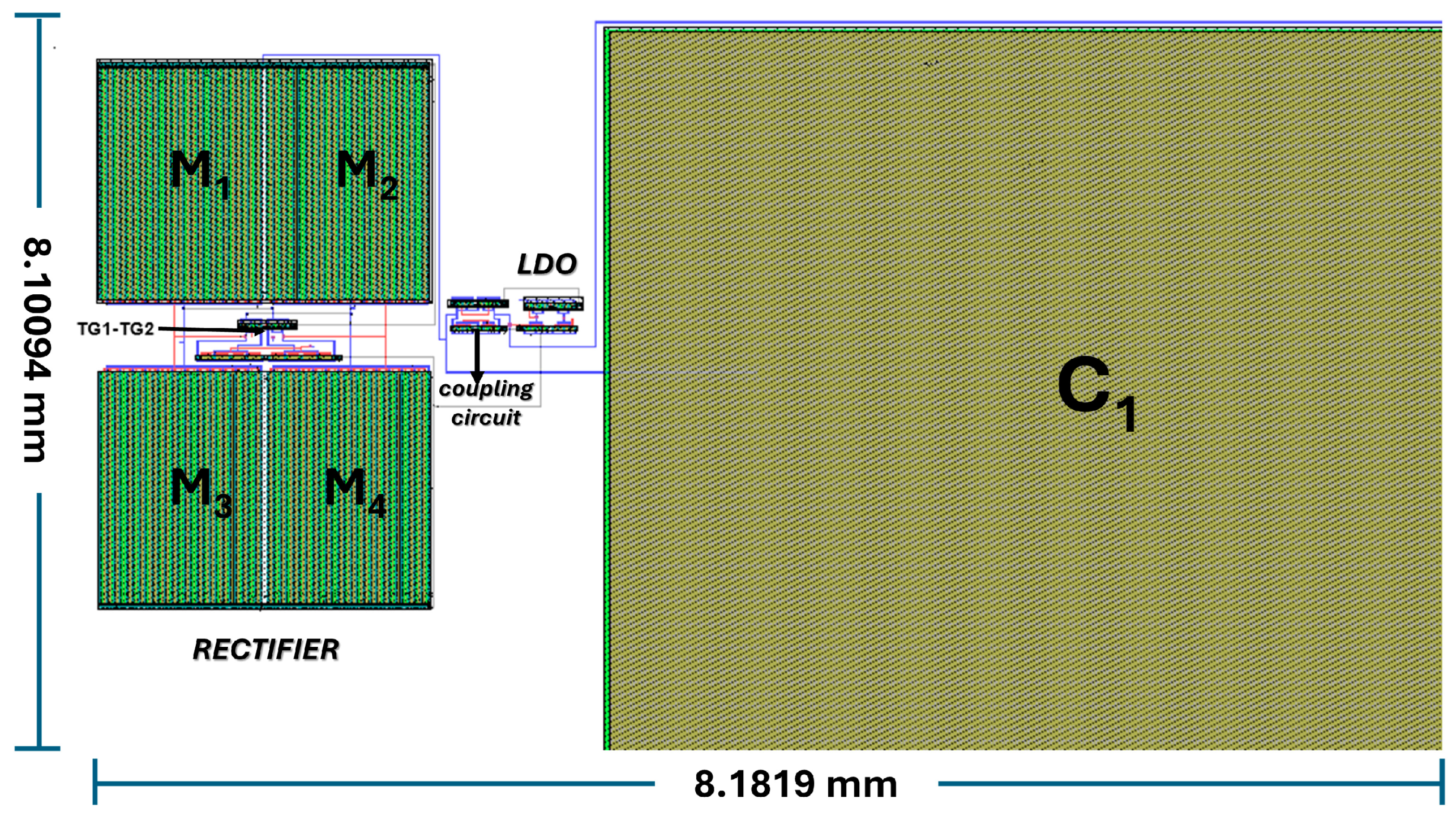
Demonstrates compact area efficiency with a silicon footprint of 66.28 mm2.
(iv)
Incorporates a coupling network that significantly reduces voltage losses between rectification and regulation stages (~10% gain).
(v)
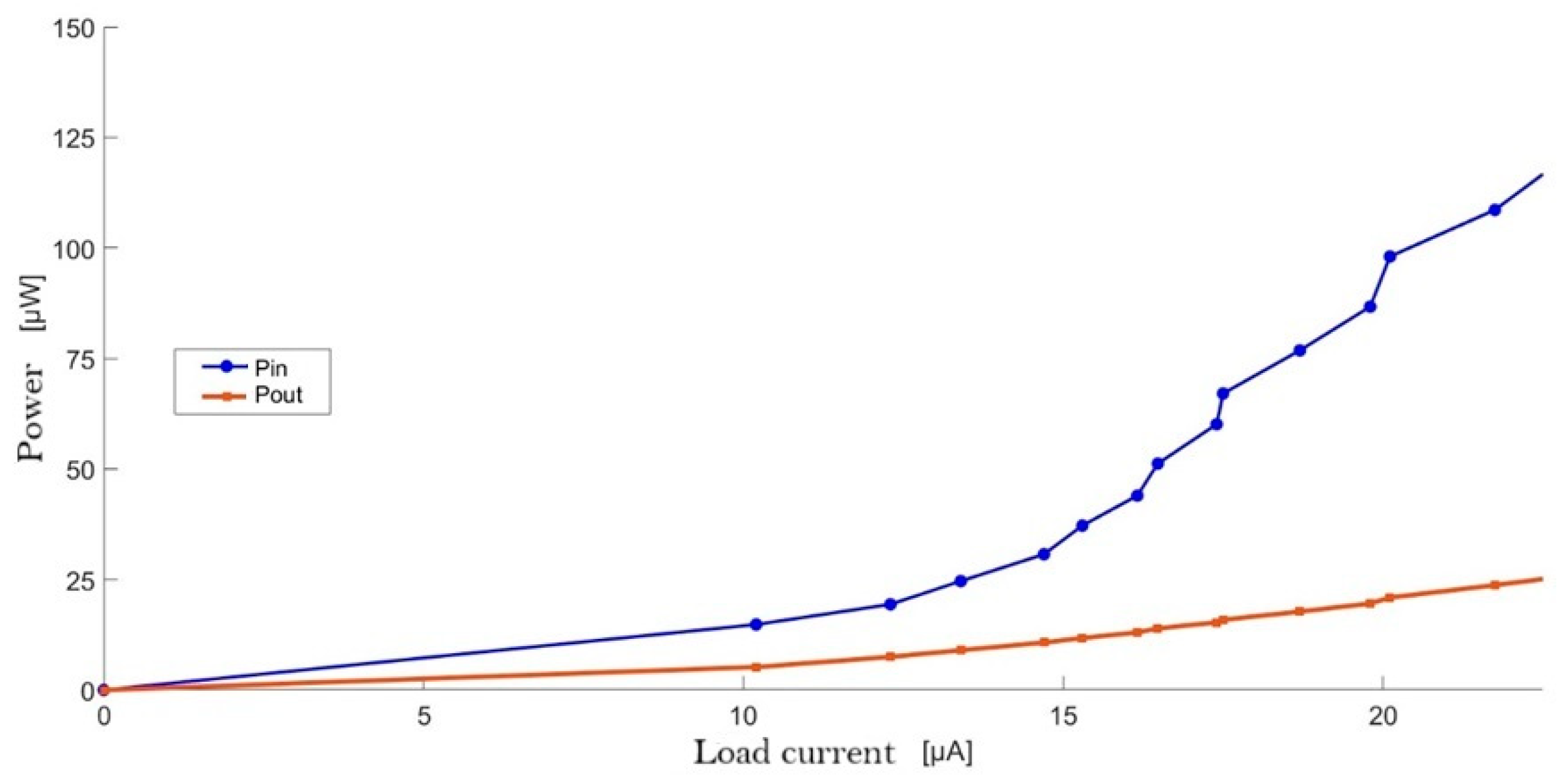
Supports power conversion efficiencies above 35% at typical load conditions for IoT sensor nodes.
Collectively, these findings address key limitations in voltage scalability, energy regulation, and circuit integration in self-powered electronic platforms.
In Section 2, we present the layout and simulation of the power management circuit of a piezoelectric energy harvester. Section 3 describes the results and discussions of the output performance of the proposed PMC. Finally, the conclusions are reported in Section 4.

2. Materials and Methods

2.1. Requirements for the IoT Sensors

For monitoring the health of patients it is required that sensors can transmit the required data through the IoT, which can contribute to the selection of better medical treatments. For instance, temperature sensors for monitoring the temperature variations in retinal prostheses [28,29] and portable glucose sensors for measuring glucose concentration in non-blood biofluids for people with diabetes [30] are IoT devices used in healthcare. Table 1 describes several low-power IoT sensors for monitoring physiological data. These devices could be portable and implantable [31], but they require clean and long-life energy sources to substitute the electrochemical batteries.
For this health monitoring, the sensors can use two devices: one in charge of processing the sensor data and another that connects the information to the user using the IoT [36,37]. As data processing components, microcontrollers with low power consumption could be used. However, this power consumption can vary depending on the selected microcontroller and the application. For instance, the power consumption of a microcontroller could be up to 13 mW [25]. Furthermore, the following wireless protocols could be used: low-power Bluetooth (power consumption between 13 mW and 15 mW), low-power Wi-Fi (power consumption from 2 mW to 800 mW), ZigBee (power consumption close to 52 mW), and radio frequency identification (power consumption approximately to 25 mW and 63 mW). This should be considered to determine the best DC-DC converter circuit for the power supply of the system.
These power constraints are especially critical in medical monitoring systems and smart home environments, where ultra-low-power, self-sustaining nodes are deployed in wearable or embedded configurations. Recent advances in ambient energy harvesting and the integration of piezoelectric and triboelectric energy harvesters have demonstrated the ability for real-time IoT sensing without battery replacement [38].

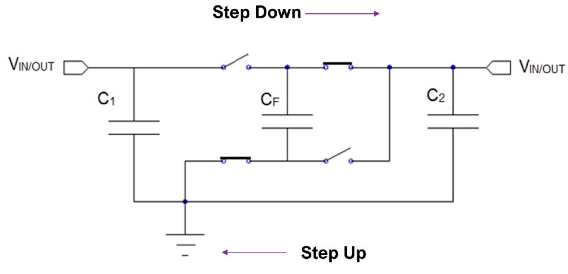
2.2. DC-DC Converter Topologies

An energy harvester has different stages before providing energy to a load. A key stage of an energy harvester is its power management circuit, in which the harvested signal is conditioned with an AC-DC rectifier and is regulated through a DC-DC converter. The optimal designs of these rectifiers and converters can increase the energy efficiency of the energy harvester systems. In this section, we will describe the different DC-DC converters that can be used with the rectifiers for the above application. The two most widely used DC-DC converter topologies for this application are linear regulators and switched-capacitor converters (SC).
In this power management, the rectified voltage must remain stable regardless of the variation that may exist in both the input signal and the circuit load [39]. One of the topologies that achieve this purpose are linear regulators. These circuits have a pass element and a MOSFET transistor (ONSEMI, Nampa, ID, USA), which will operate in the linear or saturation region. Furthermore, these circuits can control the current changes in the input signal and the connected load, which keep the required output voltage (Vout) [40]. Within this classification of linear regulators, there is the low-dropout regulator (LDO) that is the most widely used regulator for IoT sensor applications since one of its characteristics is to provide an output voltage like the input voltage. In addition, this LDO can allow for the handling of low powers on the order of a few hundred µW and input voltages of less than 2 V [41,42].
Figure 1 shows the general topology of an LDO, where there is a reference voltage (VREF), an error amplifier, the feedback network (R1 and R2), and a pass element (typically an NMOS or PMOS transistor (ONSEMI, Nampa, ID, USA)). The error amplifier controls the pass element, comparing and amplifying the reference voltage and the feedback voltage received from the voltage divider. If the feedback voltage differs to the reference voltage an error signal is generated, which is applied to control the current required in the pass element to maintain the voltage level at the required value for the load [43,44]. These regulators have a fast response on load. However, the efficiency of these regulators is low compared to Vout/Vin, but they have better integration than other low-cost converters.
LDOs are circuits that have great potential in IoT sensors. These circuits have variants such as analog topologies (ALDO), digital (DLDO), and hybrid designs (HD-LDO). The performance and efficiency of these circuits can be optimized, decreasing their area consumption [45,46]. Furthermore, switched-capacitor (SC) converters are mainly characterized for having a switch that can be a transistor. This transistor switches between the cut-off and saturation state to control the signal to ensure it is regulated. Also, this transistor has several elements to store the harvested energy, such as capacitors. These circuits can increase or decrease the voltage conversion [47,48]. DC-DC converters with capacitors have diverse topologies due to the different configurations that can be created from switches and capacitors to transfer the harvested energy to the load. Figure 2 depicts a general circuit of an SC converter. These circuits with capacitors can regulate the Vout by varying the capacitance or frequency and the direction of power delivery determines whether the converter increases or decreases the voltage. Furthermore, it depends on where the power source is located and how the energy flows [49]. Other topologies of this type of converter were shown by Ahmed et al. [50], including Dickson, Fibonacci, and Doubler, whose configurations are used as step-up converters, and the ladder topology and series-parallel, which are step-down converters. A more detailed analysis of these configurations was reported by Souza et al. [51], where the arrangements of series and parallel capacitor combinations provide different gains, efficiencies, and powers. For instance, Fibonacci presented higher gain and power levels than topologies such as Doubler, Ladder, Dickson and series-parallel due to its staged relationship; whilst the ladder topology has as a limitation related to the high output impedance, resulting in an inadequate voltage regulation for loads with high currents. On the other hand, this topology depending on its configuration can be used for both upconverter and downconverter. The Dickson topology could present a limitation for high power applications due to the low efficiency when wanting to obtain high voltage gains. However, it could work for the opposite applications.
Both LDO and SC converters have the advantage of being integrated on-chip and are suitable for low power (µW) devices, achieving high voltage conversion efficiencies of around 33–85% at Vin between 0.7 V and 2.8 V [50,52].

2.3. Power Management Circuits for Piezoelectric Energy Harvesters

The proposed PMC is designed to efficiently process the electrical output from PEHs, which typically generate low-voltage AC signals with highly variable amplitude and frequency. The PMC integrates the following three functional blocks: (1) a reconfigurable full-wave rectifier, (2) a coupling network to interface with the voltage regulator, and (3) an LDO linear regulator to provide a stable DC output.
Figure 3 depicts the proposed power management circuit for a piezoelectric energy harvester, which is integrated with a reconfigurable rectifier (cross-coupled with two transmission gates), a coupling circuit, and an LDO that has a differential pair. In addition, there is a circuit between the reconfigurable rectifier and the LDO circuit which consists of two transmission gates and a capacitor. This circuit allows the tracking of the rectifier output signal to the input of the regulator, avoiding the drop and loss of voltage from one stage to another with ~10% more efficiency in voltage ranges from 0.7 to 2 V. Without this circuit, the rectifier and the LDO have considerable voltage drop losses at the output and its optimal operation starts at 2 V. This structure can reduce forward voltage drop and improve the PCE under low input voltages.
A similar configuration has been previously explored by Paul et al. [52], who implemented a reconfigurable rectifier using 0.35 µm CMOS technology. In contrast, our circuit design employs 0.18 µm TSMC CMOS technology, integrates a coupling network, and operates in a broader voltage range (0.7–2.8 V). Thus, our circuit design is more suitable for ultra-low-power IoT applications. On the other hand, the coupling stage is implemented using a transmission gate controlled by internal signals and a coupling capacitor that serves to transfer charge to the regulator with minimal losses. This intermediate stage provides a voltage-boosting effect by reducing the transition drop between rectifier and regulator, and it allows a smoother voltage transfer that enhances the efficiency at the boundary between the two stages.
Finally, the LDO regulator ensures a stable DC output voltage under different loading and input conditions. Figure 4 shows the complete layout of the proposed PMC, considering a total silicon area of 8100.94 μm × 8181.9 μm. The interdigitated technique was used to decrease the area consumption, and a 0.18 μm CMOS technology model from TSMC was employed with 6 metal layers and one polysilicon layer and obtained from MOSIS (run: T18H). The output voltage is maintained at 1.8 V, regulated from the rectified and coupled input, with a power conversion efficiency exceeding 35% under nominal load conditions (50 kΩ).
The PMC has been verified using transient simulations in IC Nanometer Design software (version 2023.2) with corner models at typical conditions. The design demonstrates correct functionality across the intended input voltage range and provides acceptable line and load regulation. The combined architecture allows the circuit to adapt dynamically to variable energy input without requiring complex control circuitry or bulky passive components. The key electrical and physical characteristics of the proposed PMC are summarized in Table 2.
The operation of the circuit was analyzed using different input signals with a voltage range from 0.7 V to 2 V (maximum voltage provided by the reconfigurable rectifier). To avoid voltage drops, a coupling circuit is integrated with transmission gates that are controlled by the C L K and C L K ¯ signals, and a capacitor (C1) that performs the function of coupling both the AC/DC rectifier circuit and the LDO converter. It can avoid switching power losses due to a switch-capacitor that has a faster response compared to a single MOSFET transistor.

3. Results and Discussions

This section describes the results and discussions of the output performance of the proposed power management circuit, regarding its output voltage regulation, voltage conversion efficiency, and power conversion efficiency, as well as the output voltage versus input voltage.

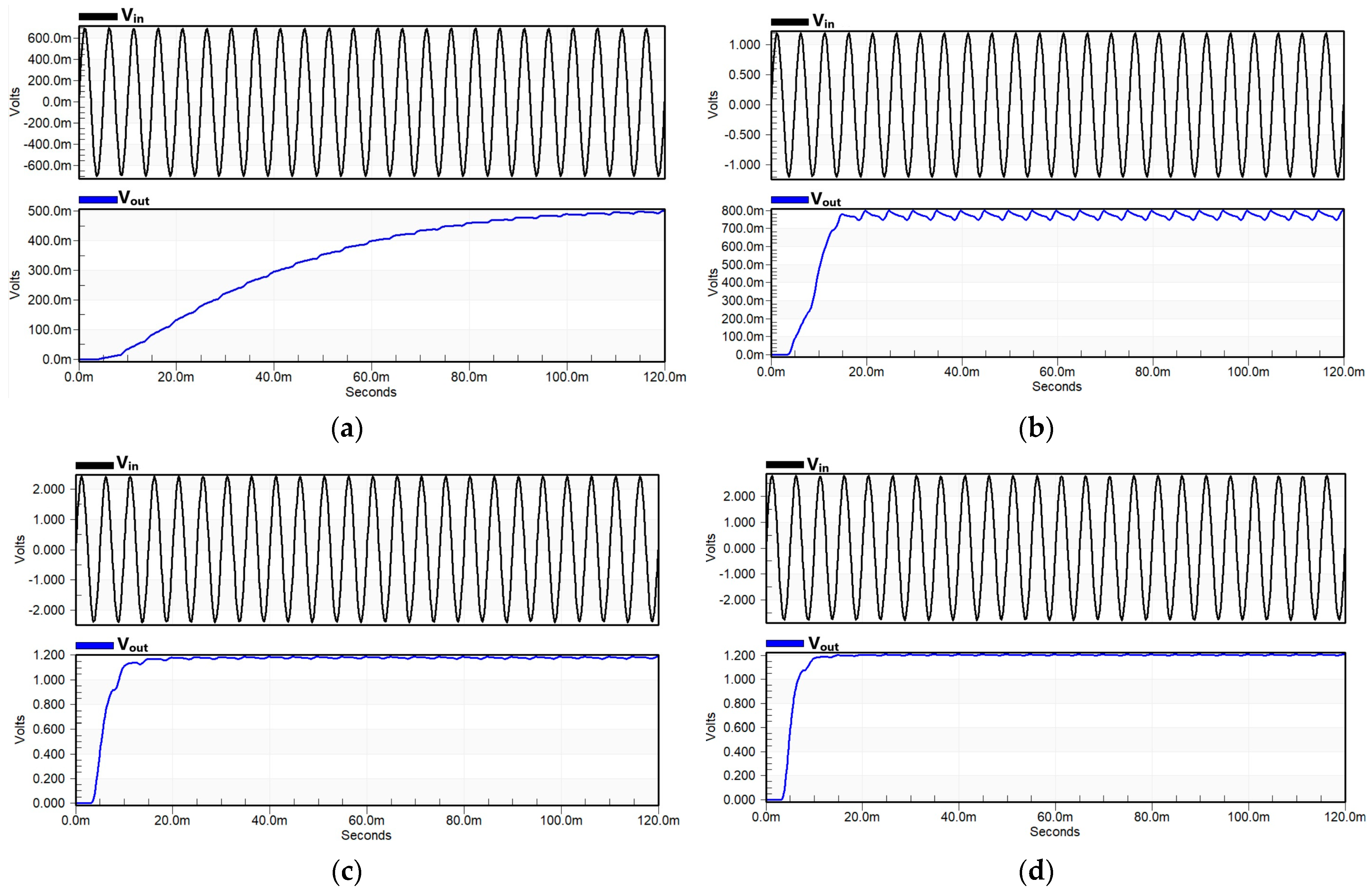
3.1. Output Voltage Regulation

Figure 5a–d illustrates the post-layout behavior of four samples of the input and output signal of the proposed PMC. Figure 5a depicts an input voltage of 0.7 V with an output voltage of 0.504 V and a voltage regulation that starts from 120 ms. For Figure 5b, there is a voltage regulation close to 20 ms with an input voltage of 1.2 V and an output voltage of 0.806 V. Figure 5c shows an input voltage of 2.5 V and an output voltage of 1.19 V, with voltage regulation close to 20 ms. On the other hand, Figure 5d registers a regulation of input voltage of 2.8 V and output voltage of 1.21 V after from 20 ms. These results allow us to predict the different ranges of optimal operation (0.7–2.8 V) in the rectifier and the LDO circuit. In addition, these results confirm the voltage regulator capability of the proposed circuit, keeping a stable output voltage. Also, no overshoot or undershoot is observed, indicating effective loop compensation.

3.2. Voltage Conversion Efficiency and Power Conversion Efficiency

The input and output signals of both voltage and current are used to determine the values of the voltage conversion efficient (VCE) and power conversion efficient (PCE) of the proposed PMC, integrating both the rectifier and the LDO with CMOS technology, respectively. These VCE and PCE parameters are obtained from the following equations [53]:
V C E = V o u t V i n × 100 %
P C E = P o u t P i n × 100 %
Thus, the performance of a power management circuit can be determined using the VCE and PCE values. Figure 6 illustrates VCE values of the proposed PMC across the input voltage sweep. The circuit achieves a peak VCE of 72.8% at 0.7 V input, gradually decreasing to 43.21% at 2.8 V. This decline is due to increasing losses in the pass devices and intrinsic resistance within the LDO and rectifier at higher voltages. However, the coupling stage minimizes transition losses, maintaining a relatively stable VCE above 40% across the full range. Based on the results of Figure 6, the VCE and highlights that at voltages below 1 V the circuit achieves efficiencies above ~73%. Figure 7 illustrates the PCE of the proposed PMC, achieving efficiencies above 35% at load currents of 10 µA under a 50 kΩ load resistance. This level of efficiency is competitive for circuits operating under ultra-low-power harvesting conditions where trade-offs between regulator stability and active loss minimization must be balanced. Thus, this power management circuit of piezoelectric energy harvesters could be used for low-power devices.
Figure 8 depicts the performance of the proposed circuit in terms of input and output power at load currents in the range of 5 µA to 30 µA. With this circuit, we could power IoT sensors that require low power. The output power increases with load resistance until a saturation point of ~150 µA, which corresponds to the regulator’s maximum designed output. Beyond this, output voltage drops due to limited current drive. The coupling capacitor improves energy delivery by storing and smoothing transitions between energy pulses.

3.3. Output Voltage as a Function of Input Voltage

Figure 9 shows a comparison of the relationship between the input and output voltages of the proposed circuit by varying different load resistors of 10 kΩ, 50 kΩ, and 100 kΩ. Better power performance can be observed at load resistances between 100 kΩ and 50 kΩ. Figure 9 illustrates Vout behavior across various input voltages and load resistances. At lower load resistances (higher current), the regulator maintains a near-constant output until the drive limit is exceeded. This result demonstrates acceptable load regulation (1.2%) and line regulation (0.5%). The output capacitor (1 µF) maintains loop stability with a simulated phase margin higher than 45°, preventing ringing or overshoot.
Table 3 summarizes key electrical characteristics, including an input voltage range between 0.7 V and 2.8 V, a regulated output voltage of 1.8 V, a maximum output current of 150 µA, and a silicon area of 66.28 mm2.
Stability analysis of the LDO circuit was performed through load and line regulation tests. The LDO circuit exhibits a line regulation of 0.5% and a load regulation of 1.2%, with a transient response time below 10 ms. The output capacitor (C1) of 1 µF ensures loop stability, maintaining a phase margin above 45° which is critical for reliable operation in variable load conditions.
To assess the relative performance of the proposed PMC, Table 4 presents a detailed comparison with recent designs from the literature. Metrics include CMOS technology node, input/output range, efficiency levels, and silicon area. The comparison indicates that the proposed PMC achieves competitive VCE and PCE across a wide input voltage range and has a compact silicon footprint. Thus, the integration of a reconfigurable rectifier, coupling network, and LDO in a single architecture contributes to its enhanced performance, making it suitable for energy-constrained IoT applications.

4. Conclusions

A CMOS-based PMC for piezoelectric energy harvesting with autonomous and low-power IoT applications is reported. The proposed power management circuit integrates the following three key functional stages: a reconfigurable full-wave rectifier, a capacitive coupling network, and a compact LDO regulator. This combination enabled efficient energy conversion, dynamic adaptability to input voltage conditions, and stable output regulation without the need for complex digital control or bulky passive components. Furthermore, post-layout simulation results, based on a 0.18 µm TSMC CMOS process, demonstrated that the circuit can support a wide input voltage range of 0.7 V to 2.8 V and regulate the output at 1.8 V. The voltage conversion efficiency (VCE) varied from 72.8% at low input voltages to 43.21% at the upper end, while power conversion efficiency (PCE) exceeded 35% under nominal load conditions. The regulator supported a maximum output current of 150 µA with a silicon area of 66.28 mm2. Compared to prior designs, the proposed PMC achieved a competitive balance of VCE, PCE, and area efficiency, while it also offered an improved modularity through a coupling stage. The layout-friendly design and stable transient behavior make it suitable for embedded systems operating under variable or intermittent energy sources, such as wearable sensors, implantable medical devices, and environmental micro-nodes.
Future research work will a full PVT corner analysis to evaluate proposed circuit robustness under process variations and thermal conditions. In addition, we will incorporate the experimental validation of the PMC through chip fabrication. Also, we will consider the optimization of the PMC for even lower quiescent current, and integration with energy-aware sensor platforms. The architecture of the PMC can also be extended to support hybrid energy harvesting schemes that combine the piezoelectric energy harvester with other transducers such as thermoelectric or triboelectric sources.

Author Contributions

Conceptualization and investigation, S.E.V.-V., R.M.W.-G., E.O.-d.-l.-R., F.L.-H. and P.A.-L.; methodology and software, S.E.V.-V. and R.M.W.-G.; formal analysis, R.M.W.-G., E.O.-d.-l.-R. and P.A.-L.; writing—review and editing, A.L.H.-M. and F.L.-H. All authors have read and agreed to the published version of the manuscript.

Funding

This work was supported by the Secretariat of Science, Humanities, Technology and Innovation (SECIHTI), Mexico, through grant 803671, and the Program of Doctorate in Applied Engineering of Universidad Veracruzana, Mexico.

Data Availability Statement

The original contributions presented in this study are included in the article. Further inquiries can be directed to the corresponding authors.

Conflicts of Interest

The authors declare no conflicts of interest.

References

  1. Han, T.; Kundu, S.; Nag, A.; Xu, Y. 3D Printed Sensors for Biomedical Applications: A Review. Sensors 2019, 19, 1706. [Google Scholar] [CrossRef] [PubMed]
  2. Mishra, S.; Rajaboina, R.K.; Jho, Y.-D. Review on the Hierarchical Improvement of Zinc Sulfide-Based Nanogenerator Systems and Their Various IoT Applications. ACS Appl. Energy Mater. 2025, 8, 1918–1941. [Google Scholar] [CrossRef]
  3. Wu, T.; Redouté, J.-M.; Yuce, M.R. A Wireless Implantable Sensor Design with Subcutaneous Energy Harvesting for Long-Term IoT Healthcare Applications. IEEE Access 2018, 6, 35801–35808. [Google Scholar] [CrossRef]
  4. Xiao, Y.; Han, Q.; Wu, N. Piezoelectric energy harvesting: A review of energy sources, structures, and working mechanisms in high-frequency excitations and operations. Smart Mater. Struct. 2025, 34, 023001. [Google Scholar] [CrossRef]
  5. Park, J.; Bhat, G.; NK, A.; Geyik, C.S.; Ogras, U.Y.; Lee, H.G. Energy per Operation Optimization for Energy-Harvesting Wearable IoT Devices. Sensors 2020, 20, 764. [Google Scholar] [CrossRef]
  6. Macário, D.; Domingos, I.; Carvalho, N.; Pinho, P.; Alves, H. Harvesting circuits for triboelectric nanogenerators for wearable applications. iScience 2022, 25, 103977. [Google Scholar] [CrossRef]
  7. Edla, M.; Lim, Y.Y.; Mikio, D.; Padilla, R. A Single-Stage Rectifier-Less Boost Converter Circuit for Piezoelectric Energy Harvesting Systems. IEEE Trans. Energy Convers. 2022, 37, 505–514. [Google Scholar] [CrossRef]
  8. Salem, L.G. A Recursive N-Path Switched-Capacitor Rectifier for Piezoelectric Energy Harvesting. IEEE J. Solid-State Circuits 2025, 60, 1461–1473. [Google Scholar] [CrossRef]
  9. Ammar, M.B.; Sahnoun, S.; Fakhfakh, A.; Kanoun, O. Design of a DC-DC Boost Converter of Hybrid Energy Harvester for IoT Devices. In Proceedings of the 2020 IEEE 6th World Forum on Internet of Things (WF-IoT), New Orleans, LA, USA, 2–16 June 2020. [Google Scholar] [CrossRef]
  10. Subasinghage, K.; Gunawardane, K.; Kularatna, N. Supercapacitor-Assisted Low-Dropout Regulator Technique for Low Output Ripple DC-DC Conversion. IEEE J. Emerg. Sel. Top. Ind. Electron. 2022, 3, 1028–1037. [Google Scholar] [CrossRef]
  11. Wang, J.; Chen, Z.; Li, Z.; Jiang, J.; Liang, J.; Zeng, X. Piezoelectric Energy Harvesters: An Overview on Design Strategies and Topologies. IEEE Trans. Circuits Syst. II Express Briefs 2022, 69, 3057–3063. [Google Scholar] [CrossRef]
  12. Shirvanimoghaddam, M.; Shirvanimoghaddam, K.; Abolhasani, M.M.; Farhangi, M.; Barsari, V.Z.; Liu, H. Towards a Green and Self-Powered Internet of Things Using Piezoelectric Energy Harvesting. IEEE Access 2019, 7, 94533–94556. [Google Scholar] [CrossRef]
  13. Pandiev, I.; Tomchev, N.; Kurtev, N.; Aleksandrova, M. Analysis of the Methods for Realization of Low-Power Piezoelectric Energy Harvesting Circuits for Wearable Battery-Free Power Supply Devices. Appl. Sci. 2024, 14, 4792. [Google Scholar] [CrossRef]
  14. Pereira-Rial, O.; Cabrini, A.; Torelli, G.; Lopez, P.; Carrillo, J.M. Ultra-Low-Power Low-Input-Voltage Charge Pump for Micro-Energy Harvesting Applications. IEEE Trans. Circuits Syst. I Regul. Pap. 2023, 70, 154–165. [Google Scholar] [CrossRef]
  15. Covaci, C.; Gontean, A. Piezoelectric Energy Harvesting Solutions: A Review. Sensors 2020, 20, 3512. [Google Scholar] [CrossRef]
  16. Long, Z.; Wang, X.; Li, P.; Wang, B.; Zhang, X.; Chung, H.S.-H. Self-Powered SSDCI Array Interface for Multiple Piezoelectric Energy Harvesters. IEEE Trans. Power Electron. 2021, 36, 9093–9104. [Google Scholar] [CrossRef]
  17. Rigo, F.; Migliorini, M.; Pozzebon, A. Piezoelectric Sensors as Energy Harvesters for Ultra Low-Power IoT Applications. Sensors 2024, 24, 2587. [Google Scholar] [CrossRef]
  18. Izadgoshasb, I. Piezoelectric Energy Harvesting towards Self-Powered Internet of Things (IoT) Sensors in Smart Cities. Sensors 2021, 21, 8332. [Google Scholar] [CrossRef]
  19. Liu, S.; Chen, S.; Gao, W.; Zhang, J.; Xu, D.; Chen, F.; Lu, Z.; Yu, X. A High-Efficiency Piezoelectric Energy Harvesting and Management Circuit Based on Full-Bridge Rectification. J. Low Power Electron. Appl. 2024, 14, 49. [Google Scholar] [CrossRef]
  20. Asthana, P.; Khanna, G. A broadband piezoelectric energy harvester for IoT based applications. Microelectron. J. 2019, 93, 104635. [Google Scholar] [CrossRef]
  21. Law, M.-K.; Jiang, Y.; Mak, P.-I.; Martins, R.P. Miniaturized Energy Harvesting Systems Using Switched-Capacitor DC-DC Converters. IEEE Trans. Circuits Syst. II Express Briefs 2022, 69, 2629–2634. [Google Scholar] [CrossRef]
  22. Wu, T.; Wu, F.; Redouté, J.-M.; Yuce, M.R. An autonomous wireless body area network implementation towards IoT-connected healthcare applications. IEEE Access 2017, 5, 11413–11422. [Google Scholar] [CrossRef]
  23. Priya, S.; Song, H.-C.; Zhou, Y.; Varghese, R.; Chopra, A.; Kim, S.-G.; Kanno, I.; Wu, L.; Ha, D.S.; Ryu, J.; et al. A review on piezoelectric energy harvesting: Materials, methods, and circuits. Energy Harvest. Syst. 2019, 4, 3–39. [Google Scholar] [CrossRef]
  24. Wang, Y.; Feng, Y.; Li, X.; Liu, Z.; Chen, C.; Cao, D.; Li, M.; Chuai, X.; Peng, Y.; Mei, X.; et al. Mutualistic symbiotic wireless node for next-era smart transportation. Nano Energy 2025, 136, 110746. [Google Scholar] [CrossRef]
  25. Wu, T.; Wu, F.; Qiu, C.; Redoute, J.M.; Yuce, M.R. A Rigid-Flex Wearable Health Monitoring Sensor Patch for IoT-Connected Healthcare Applications. IEEE Internet Things J. 2020, 7, 6932–6945. [Google Scholar] [CrossRef]
  26. Gunti, A.; Biswas, D.K.; Mahbub, I.; Adhikari, P.R.; Reid, R.C. Highly efficient rectifier and DC-DC converter designed in 180 nm CMOS process for ultra-low frequency energy harvesting applications. In Proceedings of the 2020 Dallas Circuits and Systems Conference (DCAS) 2020, Dallas, TX, USA, 15–16 November 2020. [Google Scholar] [CrossRef]
  27. Ahmed, F.U.; Sandhie, Z.T.; Chowdhury, M.H. An implementation of external capacitor-less low-dropout voltage regulator in 45 nm technology with output voltage ranging from 0.4 V–1.2 V. In Proceedings of the 2020 IEEE 38th International Conference on Computer Design (ICCD), Harford, CT, USA, 18–21 October 2020; pp. 453–456. [Google Scholar] [CrossRef]
  28. Seo, H.; Chung, W.G.; Kwon, Y.W.; Kim, S.; Hong, Y.-M.; Park, W.; Kim, E.; Lee, J.; Lee, S.; Kim, M.; et al. Smart Contact Lenses as Wearable Ophthalmic Devices for Disease Monitoring and Health Management. Chem. Rev. 2023, 123, 11488–11558. [Google Scholar] [CrossRef]
  29. Park, J.H.; Tan, J.S.Y.; Wu, H.; Dong, Y.; Yoo, J. 1225-Channel Neuromorphic Retinal-Prosthesis SoC with Localized Temperature-Regulation. IEEE Trans. Biomed. Circuits Syst. 2020, 14, 1230–1240. [Google Scholar] [CrossRef]
  30. Zhang, J.; Xu, J.; Lim, J.; Nolan, J.K.; Lee, H.; Lee, C.H. Wearable Glucose Monitoring and Implantable Drug Delivery Systems for Diabetes Management. Adv. Healthc. Mater. 2021, 10, 2100194. [Google Scholar] [CrossRef]
  31. Zhu, M.; Yi, Z.; Yang, B.; Lee, C. Making use of nanoenergy from human—Nanogenerator and self-powered sensor enabled sustainable wireless IoT sensory systems. Nano Today 2021, 36, 101016. [Google Scholar] [CrossRef]
  32. Dong, L.; Closson, A.B.; Jin, C.; Nie, Y.; Cabe, A.; Escobedo, D.; Huang, S.; Trase, I.; Xu, Z.; Chen, Z.; et al. Multifunctional Pacemaker Lead for Cardiac Energy Harvesting and Pressure Sensing. Adv. Healthc. Mater. 2020, 9, 2000053. [Google Scholar] [CrossRef]
  33. Wang, C.; Li, X.; Hu, H.; Zhang, L.; Huang, Z.; Lin, M.; Zhang, Z.; Yin, Z.; Huang, B.; Gong, H.; et al. Monitoring of the central blood pressure waveform via a conformal ultrasonic device. Nat. Biomed. Eng. 2018, 2, 687–695. [Google Scholar] [CrossRef]
  34. Gljušćić, P.; Zelenika, S.; Blažević, D.; Kamenar, E. Kinetic Energy Harvesting for Wearable Medical Sensors. Sensors 2019, 19, 4922. [Google Scholar] [CrossRef] [PubMed]
  35. Roy, S.; Azad, A.N.M.W.; Baidya, S.; Khan, F. A Comprehensive Review on Rectifiers, Linear Regulators, and Switched-Mode Power Processing Techniques for Biomedical Sensors and Implants Utilizing in-Body Energy Harvesting and External Power Delivery. IEEE Trans. Power Electron. 2021, 36, 12721–12745. [Google Scholar] [CrossRef]
  36. Mahmmod, B.M.; Naser, M.A.; Al-Sudani, A.H.S.; Alsabah, M.; Mohammed, H.J.; Alaskar, H. Patient Monitoring System Based on Internet of Things: A Review and Related Challenges With Open Research Issues. IEEE Access 2024, 12, 132444–132479. [Google Scholar] [CrossRef]
  37. Liu, Y.; Khanbareh, H.; Halim, M.A.; Feeney, A.; Zhang, X.; Heidari, H.; Ghannam, R. Piezoelectric energy harvesting for self-powered wearable upper limb applications. Nano Select. 2021, 2, 1459–1479. [Google Scholar] [CrossRef]
  38. Graham, S.A.; Manchi, P.; Paranjape, M.V.; Kurakula, A.; Kavarthapu, V.S.; Lee, J.K.; Yu, J.S. Multifunctional Thermochromic Dye-Integrated Hybrid Nanogenerators for Mechanical Energy Harvesting and Real-Time IoT Sensing. Adv. Funct. Mater. 2024, 34, 2409608. [Google Scholar] [CrossRef]
  39. Murad, S.A.Z.; Harun, A.; Isa, M.N.M.; Marzuki, A.; Sapawi, R. A Linear 0.98 mV Low-Dropout Voltage Regulator in 0.18-μm CMOS Technology. J. Phys. Conf. Ser. 2021, 1755, 012049. [Google Scholar] [CrossRef]
  40. Sobhan Bhuiyan, M.A.; Hossain, M.R.; Minhad, K.N.; Haque, F.; Hemel, M.S.K.; Md Dawi, O.; Ibne Reaz, M.B.; Ooi, K.J.A. CMOS Low-Dropout Voltage Regulator Design Trends: An Overview. Electronics 2022, 11, 193. [Google Scholar] [CrossRef]
  41. Xie, J.; Ye, D.; Wang, C.; Li, J.; Luo, Z. An adaptive Gm cell compensation technique for fast transient and high efficiency LDO without on/off-chip capacitor. AEU-Int. J. Electron. Commun. 2025, 190, 155640. [Google Scholar] [CrossRef]
  42. Zamora-Mejia, G.; Gomez-Garcia, D.E.; Giron-Nieto, H.; Martinez-Castillo, J.; Moreno-Coria, L.A.; Rocha-Perez, J.M.; Diaz-Sanchez, A. A 0.18 μm CMOS capacitor-less Low-Drop Out Voltage Regulator Compensated via the Bootstrap Flipped-Voltage Follower. Microelectron. J. 2020, 101, 104809. [Google Scholar] [CrossRef]
  43. Alicea-Morales, P.M.; Ortiz-Villanueva, C.J.; Pérez, R.; Palomera-Garcia, R.; Jiménez, M. Design of an adjustable, low voltage, low dropout regulator. In Proceedings of the IEEE International Caracas Conference on Devices, Circuits and Systems (ICCDCS) 2004, Punta Cana, Dominican Republic, 3–5 November 2004; pp. 289–292. [Google Scholar] [CrossRef]
  44. Heidrich, J.; Brenk, D.; Essel, J.; Heinrich, M.; Jung, M.; Hofer, G. Design of a low-power voltage regulator for RFID applications. In Proceedings of the 2010 IEEE Region 8 International Conference on Computational Technologies in Electrical and Electronics Engineering (SIBIRCON), Irkutsk, Russia, 11–15 July 2010; pp. 552–557. [Google Scholar] [CrossRef]
  45. Arbet, D.; Potocny, M.; Kovac, M.; Nagy, L.; Stopjakova, V. Fully On-Chip Low-Drop Regulator for Low-Power Applications. In Proceedings of the 2021 44th International Convention on Information, Communication and Electronic Technology (MIPRO), Opatija, Croatia, 27 September–1 October 2021; pp. 101–106. [Google Scholar] [CrossRef]
  46. Kilani, D.; Alhawari, M.; Mohammad, B.; Saleh, H.; Ismail, M. Reconfigurable, Switched-Capacitor Power Converter for IoT. In The IoT Physical Layer; Elfadel, I., Ismail, M., Eds.; Springer: Cham, Switzerland, 2019. [Google Scholar] [CrossRef]
  47. Kiran Kumar, G.; Kobaku, T.; Sahoo, S.; Subudhi, B.; Elangovan, D.; Blaabjerg, F. An Overview of Fully Integrated Switching Power Converters Based on Switched-Capacitor versus Inductive Approach and Their Advanced Control Aspects. Energies 2021, 14, 3250. [Google Scholar] [CrossRef]
  48. Krishnaveni, S.; Ravi, S. Effect of physical variations of inductor and capacitor on peak current in DC-DC converter. In Proceedings of the 2014 International Conference on Smart Structures and Systems (ICSSS), Chennai, India, 9 October 2014; pp. 127–130. [Google Scholar] [CrossRef]
  49. Lu, Y.; Ki, W.-H. CMOS Integrated Circuit Design for Wireless Power Transfer; Springer: Singapore, 2018. [Google Scholar] [CrossRef]
  50. Ahmed, F.U.; Sandhie, Z.T.; Ali, L.; Chowdhury, M.H. A Brief Overview of On-Chip Voltage Regulation in High-Performance and High-Density Integrated Circuits. IEEE Access 2021, 9, 813–826. [Google Scholar] [CrossRef]
  51. de Souza, A.F.; Tofoli, F.L.; Ribeiro, E.R. Switched Capacitor DC-DC Converters: A Survey on the Main Topologies, Design Characteristics, and Applications. Energies 2021, 14, 2231. [Google Scholar] [CrossRef]
  52. Paul, A.; Ramirez-Angulo, J.; Gangineni, M.; Huerta-Chua, J. Low Voltage CMOS Class AB Current Mirror/Precision Rectifier. In Proceedings of the IEEE 66th International Midwest Symposium on Circuits and Systems (MWSCAS), Tempe, AZ, USA, 6–9 August 2023; pp. 846–849. [Google Scholar] [CrossRef]
  53. Yang, C.C.; Pandey, R.; Tu, T.Y.; Cheng, Y.-P.; Chao, P.C.P. An efficient energy harvesting circuit for batteryless IoT devices. Microsyst. Technol. 2020, 26, 195–207. [Google Scholar] [CrossRef]
  54. Lin, Y.; Wu, T.; Zeng, Y.; Yang, J.; Chen, W.; Li, Z. A 15 mV-input and 71%-efficiency boost converter with 22 mV output ripple for thermoelectric energy harvesting application. Microelectron. J. 2022, 121, 105353. [Google Scholar] [CrossRef]
  55. Wu, S.-H.; Liu, X.; Wan, Q.; Kuai, Q.; Teh, Y.-K.; Mok, P.K.T. A 0.3-V Ultralow-Supply-Voltage Boost Converter for Thermoelectric Energy Harvesting with Time-Domain-Based MPPT. IEEE Solid-State Circuits Lett. 2021, 4, 100–103. [Google Scholar] [CrossRef]
  56. Jayaweera, H.M.P.C.; Pathirana, W.P.M.R.; Muhtaroğlu, A. An on-die ultra-low voltage DC–DC step-up converter with voltage doubling LC-tank. J. Micromech. Microeng. 2016, 26, 12. [Google Scholar] [CrossRef]
Figure 1. General topology of a low dropout regulator.
Nanoenergyadv 05 00007 g001
Figure 2. General topology SC converter [49].
Nanoenergyadv 05 00007 g002
Figure 3. Schematic diagram of the power management circuit for a piezoelectric energy harvester.
Nanoenergyadv 05 00007 g003
Figure 4. Schematic of the proposed CMOS power management stage for a piezoelectric energy harvester.
Nanoenergyadv 05 00007 g004
Figure 5. Post-layout simulations of the proposed power management circuit of a piezoelectric energy harvester with RLoad = 50 kΩ and frequency = 200 Hz. (a) Vin = 0.7 V, regulation starting at 120 ms, (b) Vin = 1.2 V, regulation starting at ~20 ms, (c) Vin = 2.5 V, regulation starting at 20 ms, and (d) Vin = 2.8 V, regulation starting at 15 ms.
Nanoenergyadv 05 00007 g005
Figure 6. VCE of the proposed PMC with 50 kΩ load resistance and a frequency of 200 Hz.
Nanoenergyadv 05 00007 g006
Figure 7. PCE of the proposed PMC with 50 kΩ load resistance and a frequency of 200 Hz.
Nanoenergyadv 05 00007 g007
Figure 8. Input and output power versus load current at 200 Hz frequency.
Nanoenergyadv 05 00007 g008
Figure 9. Comparison of output voltage versus input voltage at 10 kΩ, 50 kΩ, and 100 kΩ resistors.
Nanoenergyadv 05 00007 g009
Table 1. Power requirements for IoT sensors.
DeviceElectrical ParametersPower Level
Commercial pacemakers10–15 μWUltra-low [32]
Blood pressure sensors~4.6–24 mWLow [33,34]
Temperature sensors~38.5–241 µWUltra-low [34]
Pulse oximeter sensors~68 µW–4.8 mWLow [34]
Drug pump~100 μW–2 mWUltra-low [35]
Retinal stimulator~1–100 mWLow [35]
Neural stimulator~10–200 mWLow [35]
Table 2. Dimensions of the CMOS transistors of the power management circuit for a piezoelectric energy harvester.
AC/DC Rectifier TransistorsW/L (µm)FactorType
M136/0.425PMOS
M236/0.425NMOS
M336/0.425PMOS
M436/0.425NMOS
M50.5/0.184PMOS
M60.5/0.184PMOS
M70.5/24NMOS
M80.5/24NMOS
M92.5/24PMOS
M102.5/24NMOS
M112.5/24PMOS
M122.5/24NMOS
M132.5/24PMOS
M142.5/24NMOS
M152.5/24PMOS
M162.5/24NMOS
Table 3. Main parameters of the CMOS-based PMC for a piezoelectric energy harvester.
ParametersIn This Work
Technology (µm)0.18 µm TSMC
Vin (V)0.7–2.8 V
Vout (V)0.508–1.21 V
Frequency (Hz)200 Hz
VCE (%)72.57%@50 kΩ
PCE (%)35%@50 kΩ
C1 (µF)1
Area (mm2)66.28108
Table 4. Main performance parameters of different CMOS-based PMCs.
ReferenceCMOS TechnologyVin Range (V)Vout (V)VCE (%)PCE (%)Area (mm2)
This Work0.18 µm0.7–2.81.843–72.83566.28
Gunti et al. [26]0.18 µm0.5–2.01.250–7025–3570
Ahmed et al. [27]0.45 µm0.4–1.21.035–6020–3060
Paul et al. [52]0.18 µm1.0–2.51.840–6530–4080
Yihan et al. [54]0.18 µm0.15–2.41.2545–7130–3865
Liu et al. [19]0.11 µm0.5–2.51.850–7540–500.6
Wu et al. [55]0.13 µm0.30.372281.16
Jayaweera et al. [56]0.18 µm0.201.615–3532–401.15
Disclaimer/Publisher’s Note: The statements, opinions and data contained in all publications are solely those of the individual author(s) and contributor(s) and not of MDPI and/or the editor(s). MDPI and/or the editor(s) disclaim responsibility for any injury to people or property resulting from any ideas, methods, instructions or products referred to in the content.

