1. Introduction
Thermoelectric (TE) materials, as a series of functional materials, can convert temperature differences into electrical potentials, or vice versa [
1,
2,
3]. Thus, devices fabricated from TE materials are widely investigated by researchers to solve the issues like heat recovery, room-temperature power generation, or self-charging power sources [
4,
5,
6]. Typically, the efficiency of the TE devices is determined by the intrinsic properties of the TE materials, which are evaluated by the dimensionless figure of merit,
zT (
zT =
S2σT∕
κ, where
S,
σ,
T, and
κ are the Seebeck coefficient, electrical conductivity, absolute temperature, and total thermal conductivity, respectively) [
7,
8]. To fabricate TE devices for the applications of room-temperature power generation or self-charging power sources, forming TE materials into thin films [
9] and employing flexible substrates, like polyimide (PI) [
10], etc., are two effective strategies for researchers to enhance flexibility, though sometimes leading to a slight reduction in thermoelectric performance [
9]. However, considering that the thermal conductivity (
κ) values of thin films are difficult to measure accurately, the power factor (
PF =
S2σ) is commonly used to assess their TE performance potential [
11]. The literature reports that intrinsic Ag
2Se thin films typically exhibit
κ values around 1.20 to 1.35 W·m
−1·K
−1, located in the range of approximately 1.9 to 2.2 of Ag/Se ratio [
12]. In addition,
S and
σ are coupled with the carrier concentration (
n), which shows that the increase in n leads to the increase in σ and the decrease in S [
13,
14]. Thus, the simultaneous increase in S and
σ is also a challenge for researchers to enhance the TE performance of flexible thin films.
Over the past several decades, near-room-temperature TE materials, such as Bi
2Te
3 and Sb
2Te
3, have been extensively studied. In recent years, considerable efforts have been devoted to exploring new material systems with high TE performance near room temperature, with particular attention given to silver and silver–copper chalcogenides (Ag
2Q and AgCuQ, where Q = S, Se, and Te) [
15,
16]. Specifically, Ag
2Se thin films exhibit comparable
n-type TE performance to that of mature Bi
2Te
3, showing high
σ and low
κ near room temperature [
17]. Moreover, the abundance of Ag
2Se in the Earth’s crust and its environmental compatibility make it a promising alternative to Bi
2Te
3 [
18]. Furthermore, Ag
2Se possesses a relatively narrow band gap (~0.02 eV to 0.22 eV), demonstrating huge potential for the enhancement of TE performance [
15]. Although Ag
2Se possesses a relatively stable orthorhombic structure near room temperature, a phase transition occurs when the temperature reaches approximately 130 °C [
18]. Thus, Ag
2Se thin films are typically measured in the temperature range of room temperature to 100 °C. According to various reports on Ag
2Se TE thin films, multiple methods have been developed for the fabrication of high-performance Ag
2Se thin films, such as adjusting the Ag/Se ratio (e.g., Ag
1.8Se [
19] and Ag
2.06Se [
20]), texturing (e.g., (00l)-oriented [
21] and (013)-oriented texturing [
22]), and doping (e.g., Te [
21], Ga [
23], and S [
24]).
In this work, we synthesized Ag
2Se thin film samples by a widely utilized magnetron sputtering method under different sputtering power settings, followed by a post-deposition annealing process at different annealing temperatures. Magnetron sputtering was selected due to its suitability for precise parameter control, high film uniformity, and compatibility with flexible substrates. In addition, post-deposition annealing was performed to enhance the crystallinity and phase purity of the Ag
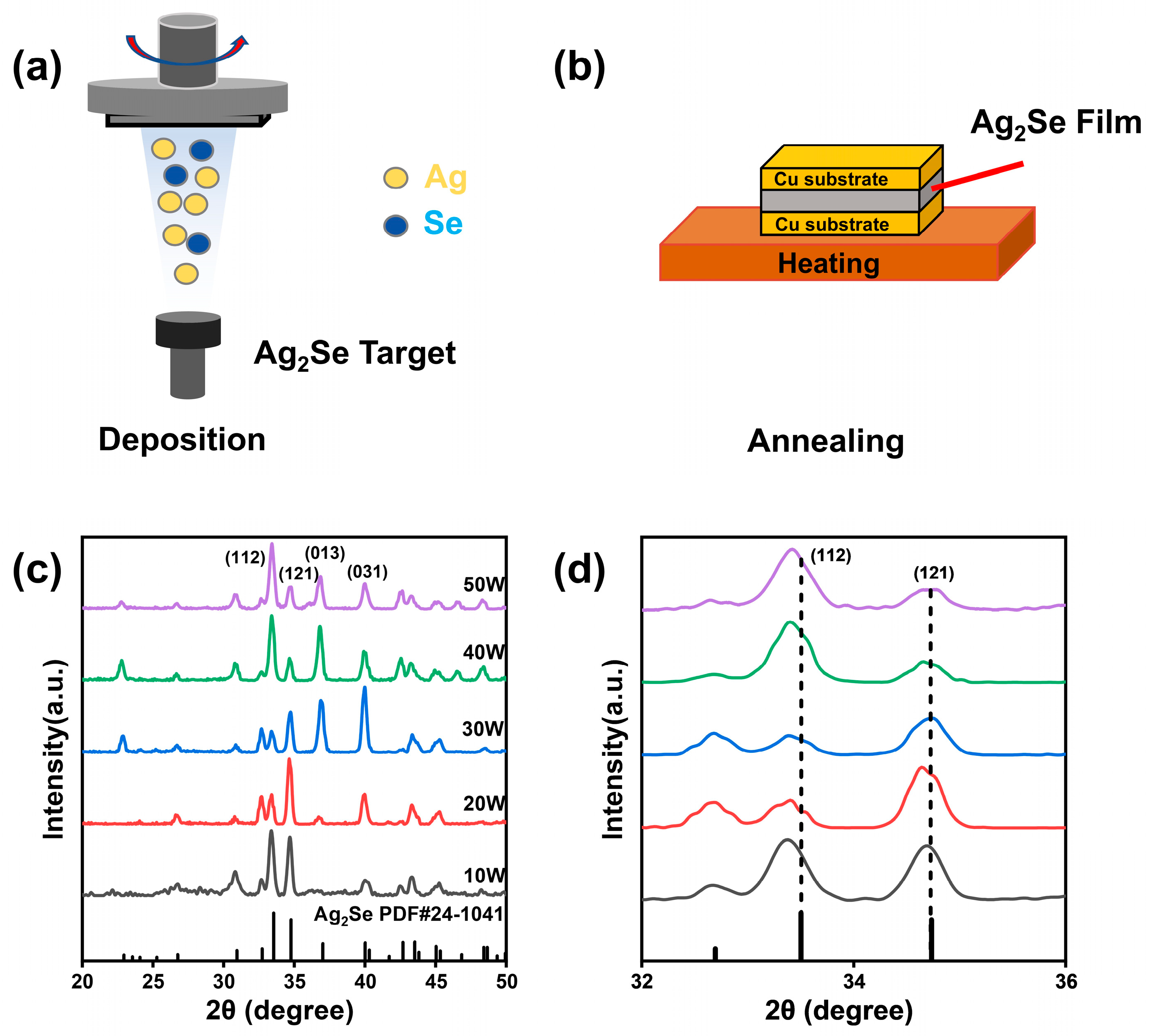
2Se thin films, addressing how sputtering power and annealing temperature affected TE performance. The schematic diagrams of the magnetron sputtering process and the post-deposition annealing process are shown in
Figure 1a and 1b, respectively. The aim of this work was to synthesize high-performance flexible Ag
2Se thin films by magnetron sputtering followed by post-deposition annealing. Moreover, the influence of sputtering power and annealing temperature on TE performance was systematically investigated based on the crystal structure and microstructural analysis.
2. Materials and Methods
Thin film fabrication: Firstly, the polyimide (PI) substrates were cut into chips with the size of 20 mm × 20 mm × 0.12 mm and ultrasonically and sequentially cleaned in deionized water, ethanol, and acetone, with 20 min for each step. The PI substrates were chosen for their high mechanical and thermal stability, which enabled post-deposition annealing without degradation. Moreover, the flexibility of the PI substrate is outstanding, making it widely used in flexible TE device fabrication [
21,
22]. Secondly, Ag
2Se thin films were deposited on PI substrates using the magnetron sputtering technique. As shown in
Figure 1a, the Ag
2Se target material (99.99% purity, Zhongnuo Advanced Material Co., Ltd., Beijing, China) was loaded into the vacuum chamber, which was evacuated to a pressure below 3.0 × 10
−3 Pa. During the deposition process of Ag
2Se thin films, the working pressure was maintained at 0.5 Pa with an argon (Ar) flow rate of 40 sccm. The sputtering power of this process was set to 10 W, 20 W, 30 W, 40 W, and 50 W to further investigate the effect of sputtering power on TE performance.
Post-deposition annealing: The synthesized 30 W sample of Ag
2Se thin films were sandwiched between the Cu substrates and placed on the heater, as shown in
Figure 1b. The annealing environment is in vacuum with a glove box at the annealing temperature for 30 min, followed by another 30 min to maintain the temperature, and an automatic decrease to room temperature. The annealing temperatures of the thin film samples were set to 150 °C, 200 °C, 250 °C, 300 °C, and 350 °C to investigate the effect of annealing temperature on TE performance.
Characterization: X-ray diffraction (XRD, D/max-2500, Rigaku Corporation, Tokyo, Japan) was used to characterize the crystal structure of the synthesized samples with a scanning range of 2θ = 10° to 50° and a scanning speed of 10°/min. The distribution and analysis of the valence states of elements were detected by an X-ray photoelectron spectroscope (XPS; ESCALAB Xi+, Thermo Fisher, Waltham, MA, USA). The surface and cross-sectional morphology of the synthesized samples were observed by field-emission scanning electron microscopy (SEM, Supra 55 Sapphire, Zeiss, Oberkochen, Germany), and the elemental composition was analyzed by the equipped energy dispersive X-ray spectrometer (EDS, BRUKER QUANTAX 200, Zeiss, Oberkochen, Germany). The high-resolution nanostructure of the synthesized samples was characterized by a spherical aberration-corrected transmission electron microscope (AC-TEM, Titan3 Themis G2, FEI, Hillsboro, CA, USA). The S and σ of the synthesized samples were measured using an SBA apparatus (SBA458, Netzsch, Selb, Germany). The carrier concentration (n) and carrier mobility (μ) at room temperature were measured by a Hall measurement system (HL5500PC, Nanometrics, Milpitas, CA, USA). The thickness of the synthesized thin films was measured by a surface-profile measurement system (Dektak XT, Bruker, Billerica, MA, USA).
3. Results and Discussions
Figure 1d shows the X-ray diffraction (XRD) patterns of Ag
2Se TE thin films with different sputtering power settings of 10 W, 20 W, 30 W, 40 W, and 50 W from 2θ = 20° to 50°, respectively. All the diffraction peaks of the samples can be well indexed to the standard PDF card (PDF#24-1041) of the orthorhombic β-Ag
2Se phase without impurity peaks detected, confirming the high purity in the phases and crystallinity of all the synthesized samples. Although all the samples exhibit the (013) diffraction peak, its intensity increases significantly at intermediate sputtering powers (particularly at 30 W and 40 W), suggesting a progressive enhancement of preferential orientation along the (013) plane rather than a uniform growth behavior across all conditions [
22]. In addition, the 30 W sample shows the strongest (013) characteristic peak, which is associated with the higher crystallinity and
μ [
18,
25].
Figure 1d shows the enlarged XRD patterns of the (112) and (121) characteristic peaks of the synthesized samples from 32° to 36°. Both the (112) and (121) characteristic peaks shift to the lower angle, pointing out the expansion of the lattice in the synthesized samples. The calculated lattice parameters of the synthesized samples are listed in
Table S1. According to the lattice parameters and the lattice volume, the expansion of the lattice can be observed, which agrees with the conclusion by the XRD patterns.
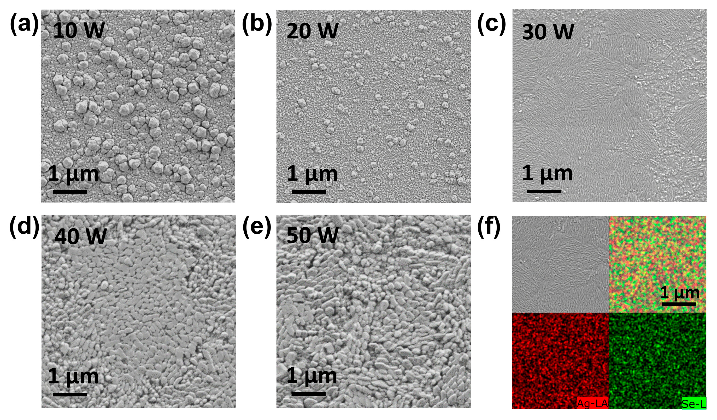
To better understand the surface morphology and crystallinity of the synthesized samples, scanning electron microscopy (SEM) was performed, as shown in
Figure 2a–e. The observed SEM images, supported by the EDS results in
Figure 2f, indicate the uniformly distributed elemental consistent of the Ag
2Se phase. Specifically, the 30 W sample shows a denser and more uniform microstructure than the other samples with high crystallinity. Moreover, the 10 W and 20 W samples show Ag-rich clusters. In contrast, the surfaces of the 40 W and 50 W samples become dense and continuous. These results suggest that the increase in sputtering power initially suppresses the Ag-rich clusters and promotes the formation of a dense Ag
2Se phase but leads to surface disorder beyond 30 W. In addition, the increase in sputtering power also strengthens the preferential growth of (013), resulting in a denser Ag
2Se phase up to 30 W. Notably, the 30 W sample has the closest Ag/Se atomic ratio to 2.02. Beyond this power, the Ag/Se atomic ratio of all the samples, listed in
Table S2, decreased with increasing sputtering power, indicating the consistent tendency with the SEM observations. The cross-sectional SEM morphology of the representative Ag
2Se thin film is shown in
Figure S1. The average thickness values of the synthesized Ag
2Se thin films are listed in
Table S3.
Figure 3 shows the temperature-dependent
σ (a),
S (b),
n and
μ (c),
PF (d) of all the synthesized Ag
2Se thin film samples at room temperature. In
Figure 3a,
σ first increased with increasing sputtering power, reaching a maximum value of 30 W, and then decreased. In
Figure 3b, the absolute value of
S first increased with increasing sputtering power up to 40 W, followed by a decrease at 50 W. All the
S values shown in the figure are negative, confirming the successful fabrication of n-type Ag
2Se thin films. In
Figure 3c, the carrier concentration (
n) and carrier mobility (
μ) correlated well with the tendency of
S and
σ, which also confirms the XRD results of the better
μ in the 30 W sample.
Figure 3d demonstrates the
PF value with different sputtering power settings. The maximum
PF value of 7.0 µW·cm
−1·K
−2 at room temperature is achieved by the 30 W sample. Thus, the simultaneous enhancement of
S and
σ can be achieved by tuning the sputtering power up to 30 W, pointing out the successful decoupling of these two parameters. Moreover, TE performance results are also consistent with the SEM observations and Ag/Se ratio results, further confirming the reliable tendency and results in TE performance. However, the
PF values are low even compared to our previous work [
20,
21,
22]. Thus, we further conducted post-deposition annealing to enhance the TE performance of Ag
2Se thin films.
After identifying the thin film sample with the highest
PF value of different sputtering power settings, the 30 W sample was then subjected to post-deposition annealing treatment to improve its microstructure and further affect the TE performance [
19,
21]. The annealing temperatures were set to 150 °C, 200 °C, 250 °C, 300 °C, and 350 °C.
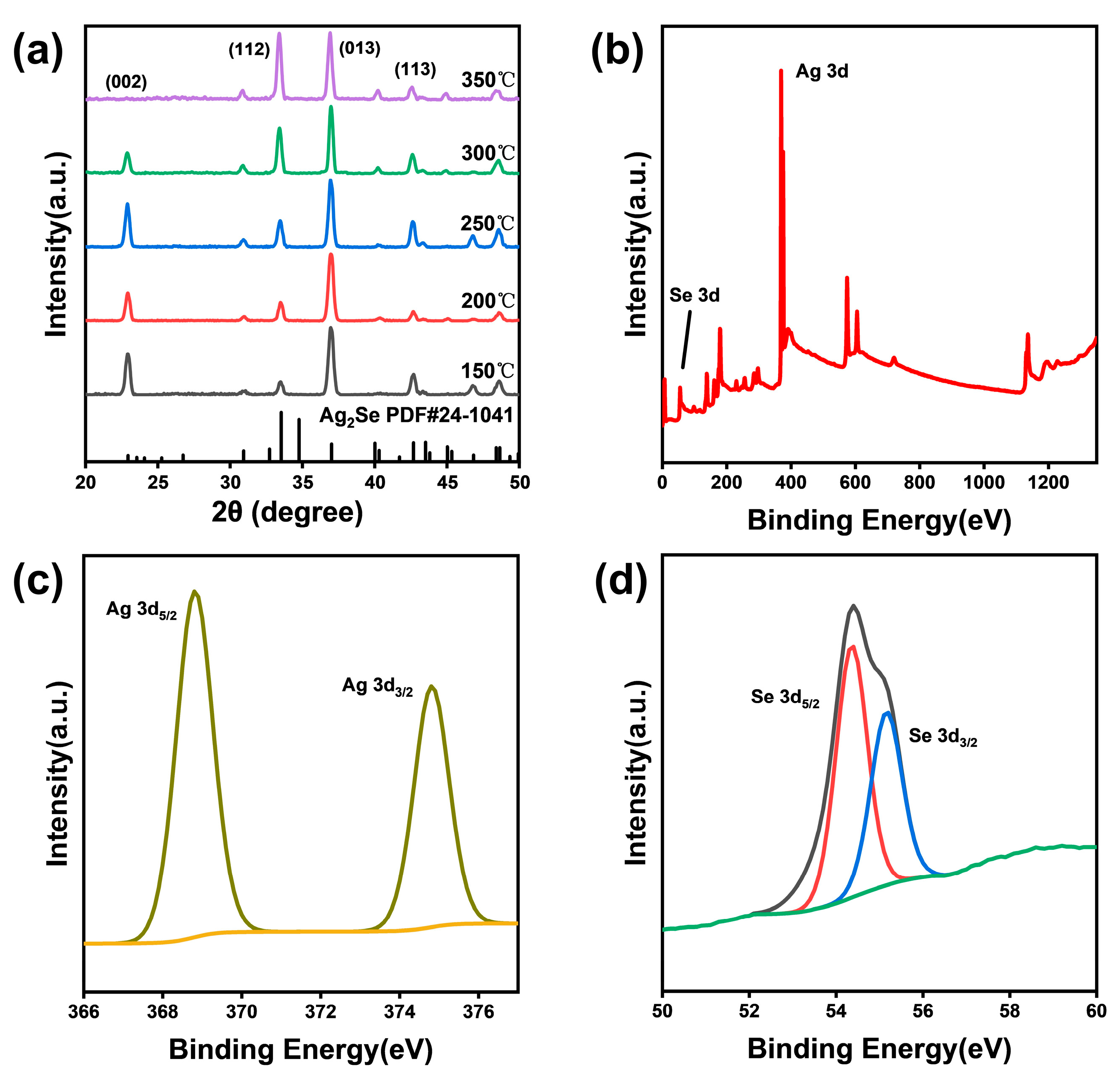
Figure 4a shows the XRD patterns of the annealed Ag
2Se thin film samples from 2θ = 20° to 50°. All the observed diffraction peaks can be well indexed to the standard PDF card (PDF#24-1041) of Ag
2Se without significant impurity peaks, pointing out the relatively pure phase of the orthorhombic β- Ag
2Se phase possessed by the annealed samples. Compared to the samples without annealing shown in
Figure 1d, (002), (112), and (113) characteristic peaks appeared with significantly high intensity.
In addition to XRD analysis, X-ray photoelectron spectroscopy (XPS) analysis was employed to further investigate the elemental valence states in the 30 W sample annealed at 300 °C. According to the spectrum in
Figure 4c, the Ag 3
d spectrum exhibits two distinct peaks of Ag
3d3/2 and Ag 3
d5/2 located at approximately ~374.8 eV and ~368.8 eV, respectively, indicating the presence of the Ag
+ oxidation state without the detectable metallic Ag state. In
Figure 4d, the Se 3
d spectrum reveals two peaks of Se 3
d3/2 and Se 3
d5/2 located at ~55.2 eV and ~54.4 eV, respectively, pointing out the existence of Se
2- species. These results confirm the formation of Ag
2Se with high purity and stable elemental valence states.
To further investigate the nanostructure of Ag
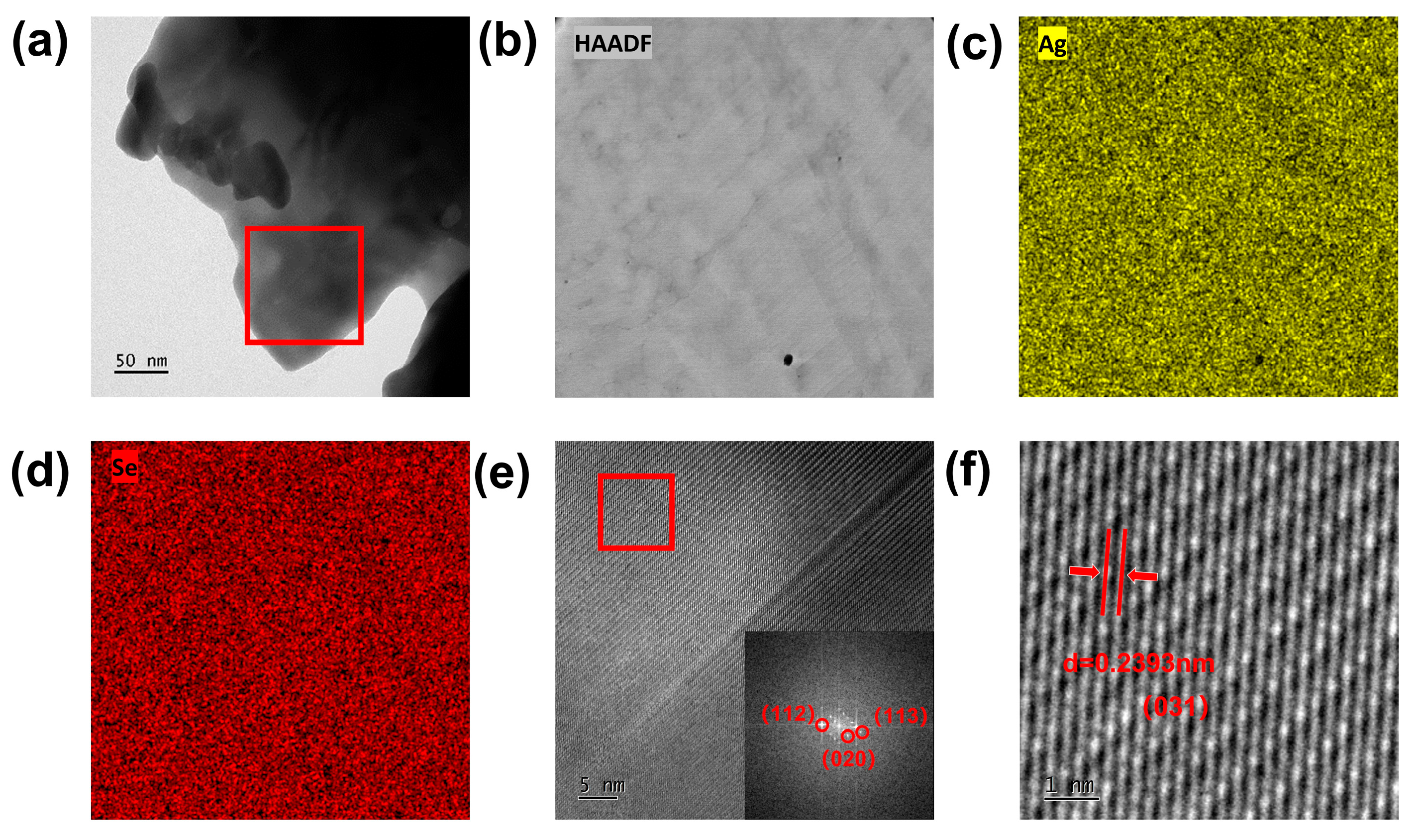
2Se thin films, the 30 W sample annealed at 300 °C was then studied by a transmission electron microscope (TEM).
Figure 5a shows a low-resolution TEM image of the 30 W sample annealed at 300 °C, with a well-crystallized structure.
Figure 5b is the high-resolution, high-angle annular dark field (HR-HAADF) image of the red circled area in
Figure 5a.
Figure 5c,d present the EDS mapping of the observed area in
Figure 5b with Ag and Se elemental analyses, respectively. As the figures show, the annealed sample exhibits a highly ordered Ag
2Se phase without any impurity phases or clusters.
Figure 5e shows the atomic-scale HR-TEM image of the rectangular area in
Figure 5b with the inset of the fast Fourier transform (FFT) image.
Figure 5f presents the observed image of the red rectangle area in
Figure 5e. As the figure shows, the atomic distributions are uniform and neatly organized. The d-spacing of the observed area was calculated as 0.2393 nm, which corresponds to the (031) plane in standard Ag
2Se. Post-deposition annealing can increase the crystallinity by suppressing the formation of Ag-rich clusters and re-organizing the nanostructure to the dense and pure Ag
2Se phase. In summary, these results demonstrate the successful synthesis of high-quality Ag
2Se thin films by magnetron sputtering and post-deposition annealing, with a well-ordered nanostructure and high crystallinity at the atomic scale.
Finally, the annealed Ag
2Se thin film samples were measured by the ZEM-3 and LFA instruments to analyze TE properties.
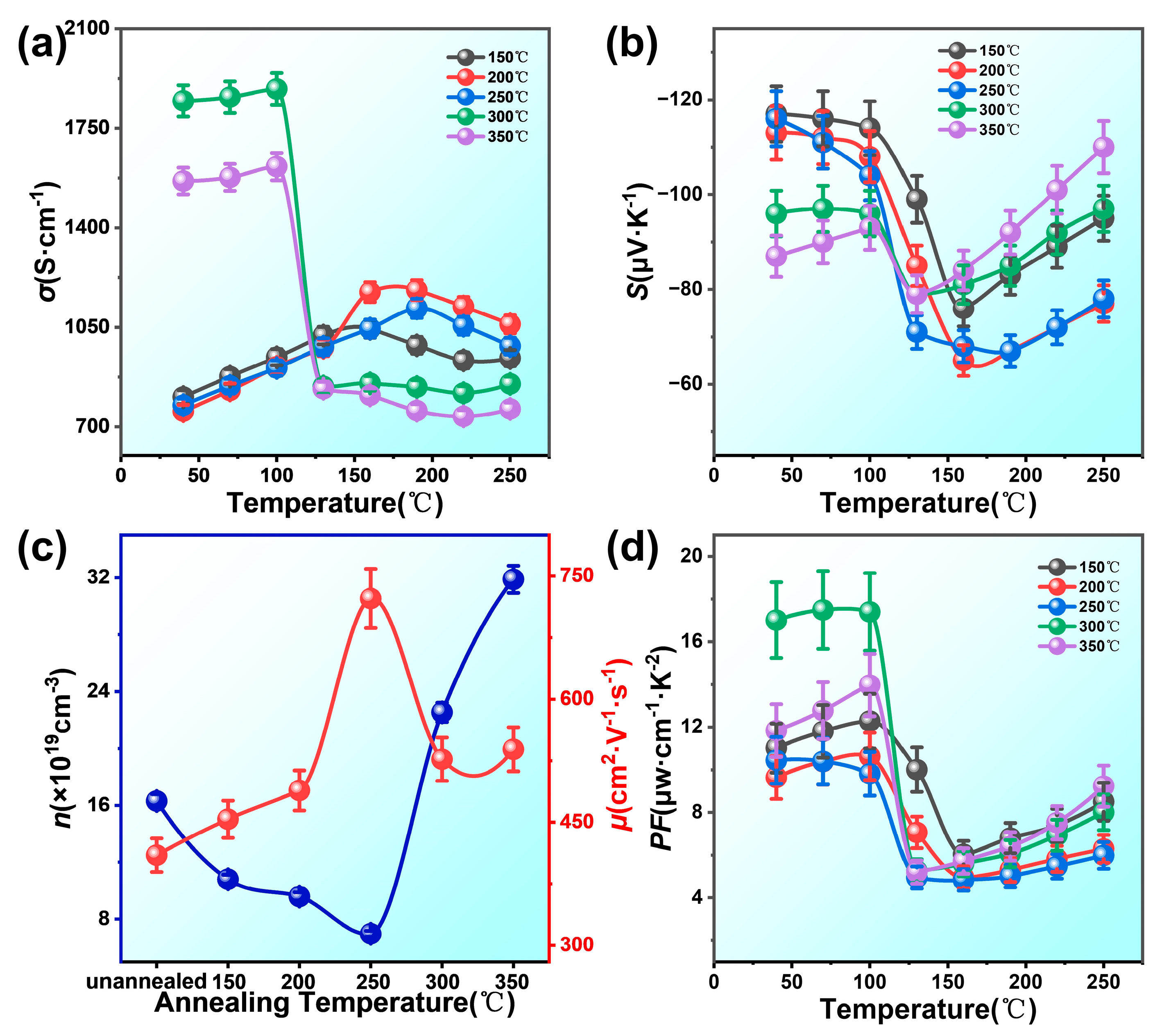
Figure 6 shows the temperature-dependent
σ (a),
S (b),
n, and
μ (c), and
PF (d) at different annealing temperatures. Since the phase transition happened at around 130 °C, the diagrams can be divided into two temperature regions: from room temperature to 100 °C (orthorhombic Ag
2Se) and from 150 °C to 250 °C (cubic Ag
2Se). Most of the reports only consider the orthorhombic temperature region since TE performance decreases sharply after the phase transition [
21,
22]. In the orthorhombic Ag
2Se temperature area in
Figure 6a,
σ increases with the increasing temperature. The 30 W sample annealed at 300 °C exhibits the highest
σ at 100 °C among all the annealed samples. The samples annealed at 300 °C and 350 °C exhibit relatively high
σ in the orthorhombic Ag
2Se temperature area but decreased sharply in the cubic Ag
2Se temperature region. In
Figure 6b, the absolute value of
S in most of the annealed samples decreased during the phase transition and then increased with further temperature rises. In addition, the negative
S values also indicate
n-type Ag
2Se after post-deposition annealing.
Figure 6c shows the
n and
μ of the annealed samples at room temperature. These trends are consistent with the variations in
σ and
S observed in
Figure 6a and 6b, respectively.
Figure 6d illustrates that the
PF values of the annealed samples are temperature-dependent. All the
PF values also decreased sharply after the phase transition temperature, showing that the
PF values in orthorhombic Ag
2Se consistently exhibit higher TE performance than cubic Ag
2Se. The 30 W sample annealed at 300 °C possesses the highest
PF values of around ~17.4 µW·cm
−1·K
−2 at 100 °C. Finally, the 30 W sample annealed at 300 °C was served as n-leg, with p-leg Sb
2Te
3 used to fabricate a flexible TE generator. The measured output voltage (
U) and output power (
P) of this device as a function of current (I) with the temperature difference Δ
T (set as 5, 15, 25, 35, 45, and 55 K) are shown in
Figure S2. The maximum
U and
P are ~140.3 mV and ~6530.0 nW under the Δ
T of 55 K. Moreover, the calculated power density is around 181.4 W·m
−2 in the fabricated f-TEG.
