Article

SCAPS-1D Simulation of Various Hole Transport Layers’ Impact on CsPbI2Br Perovskite Solar Cells Under Indoor Low-Light Conditions

Department of Mechatronics Engineering, National Changhua University of Education, Changhua 50007, Taiwan
*
Author to whom correspondence should be addressed.
Solids 2025, 6(3), 31; https://doi.org/10.3390/solids6030031 (registering DOI)
Submission received: 9 May 2025 / Revised: 13 June 2025 / Accepted: 20 June 2025 / Published: 21 June 2025

Abstract

:
This study presents the first comprehensive theoretical investigation utilizing SCAPS-1D simulation to systematically evaluate eight hole transport materials for CsPbI2Br perovskite solar cells under authentic indoor LED conditions (560 lux, 5700 K color temperature). Unlike previous studies employing simplified illumination assumptions, our work establishes fundamental design principles for indoor photovoltaics through rigorous material property correlations. The investigation explores the influence of layer thickness and defect concentration on performance to identify optimal parameters. Through detailed energy band alignment analysis, we demonstrate that CuI achieves superior performance (PCE: 23.66%) over materials with significantly higher mobility, revealing that optimal band alignment supersedes carrier mobility under low-light conditions. Analysis of HTL and absorber layer thickness, bulk defect concentration, interface defect density, and an HTL-free scenario showed that interface defect concentration and absorber layer parameters have greater influence than HTL thickness. Remarkably, ultra-thin HTL layers (0.04 μm) maintain >99% efficiency, offering substantial cost reduction potential for large-scale manufacturing. Under optimized conditions of a 0.87 μm absorber layer thickness, defect concentration of 1015 cm−3, interface defect concentration of 109 cm−3, and CuI doping concentration of 1017 cm−3, PCE reached 28.57%, while the HTL-free structure achieved 17.6%. This study establishes new theoretical foundations for indoor photovoltaics, demonstrating that material selection criteria differ fundamentally from outdoor applications.

1. Introduction

Increasing environmental awareness has elevated the importance of solar energy harvesting technologies. Among various solar cell technologies, perovskite solar cells (PSCs) have garnered significant attention due to their outstanding photoelectric conversion efficiency, low manufacturing cost, and excellent photoelectric properties [1,2]. However, conventional solar energy generation faces limitations, including the inability to generate power after sunset and susceptibility to weather conditions. Indoor low-light energy harvesting presents a promising solution to overcome these limitations. Recent studies have shown that perovskite solar cells can achieve high power conversion efficiencies under indoor lighting conditions, making them promising candidates for powering Internet of Things (IoT) devices [3]. Yang et al. demonstrated that optimized perovskite compositions can maintain a stable performance under various indoor lighting spectra including LED, fluorescent, and halogen sources [4]. Recent experimental validation by multiple research groups has confirmed the exceptional potential of CsPbI2Br for indoor applications, yet systematic theoretical frameworks for optimal device design remain underdeveloped. For effective indoor light harvesting under common sources such as LEDs, solar cells require bandgaps of approximately 1.9 eV [2]. CsPbI2Br, with a bandgap of 1.88 eV [5], emerges as an ideal absorber layer material for indoor low-light photovoltaic applications. Most critically, previous computational studies have employed oversimplified illumination conditions that fail to capture the unique spectral and intensity characteristics of actual indoor environments. Despite the growing interest in indoor photovoltaics, systematic studies comparing different hole transport layers specifically for CsPbI2Br under realistic indoor LED conditions remain limited. This work addresses this critical gap by providing the first comprehensive evaluation of HTL materials under authentic indoor illumination conditions (560 lux white LED, 5700 K color temperature), which closely mimic real-world indoor environments where these devices would operate. The thermal and phase stability of CsPbI2Br has been significantly improved through various strategies including compositional engineering and interface modification [6]. Comparative studies have shown that CsPbI2Br maintains its black phase at room temperature longer than CsPbI3, while still offering a suitable bandgap for both outdoor and indoor applications [7]. Recent experimental studies by Bahadur et al. [8] demonstrated that CsPbI2Br-based devices achieved power conversion efficiencies exceeding 20% under 1000 lux fluorescent lighting, highlighting their practical potential for indoor applications. Liu et al. [9] further improved device stability through compositional engineering, addressing a critical challenge in perovskite technology.
Unlike its performance under standard AM 1.5G illumination where conversion efficiency typically ranges between 17 and 19%, CsPbI2Br-based solar cells demonstrate superior performance under indoor lighting conditions, with potential photoelectric conversion efficiencies reaching up to 34.2% when paired with appropriate HTLs [10]. Experimental work by Wang et al. [11] confirmed this trend, showing that optimized CsPbI2Br devices maintained over 90% of their initial efficiency after 1000 h under continuous indoor illumination, outperforming their outdoor stability metrics. While the absorber layer plays a crucial role in determining efficiency, the electron transport layer (ETL) and HTL significantly impact overall device performance. Traditionally, TiO2 has been widely employed as an ETL, but its instability and high-temperature processing requirements have led to the consideration of SnO2 as a superior alternative due to its enhanced photoelectric stability and low-temperature processing compatibility. Hoang Huy et al. [12] experimentally validated this transition, demonstrating that SnO2-based devices exhibited 15% higher stability under operational conditions compared to TiO2 counterparts. The fundamental functions of HTLs include hole extraction and transport, the prevention of electron flow toward the anode, and protection of the perovskite layer from moisture and oxygen [13]. Recent research has focused on developing low-cost, dopant-free hole transport materials that can enhance both the efficiency and stability of perovskite solar cells [14]. Additionally, inorganic hole transport layers have gained attention for their superior environmental stability compared to organic counterparts, potentially enabling longer device lifetimes under various operating conditions [15].
Device simulation software like SCAPS-1D (version 3.3.11) provides a cost-effective approach to optimize solar cell structures and identify promising material combinations before experimental validation. Beyond SCAPS-1D, researchers have employed various simulation tools to model perovskite solar cell performance, including finite element analysis and drift-diffusion modeling [16]. These complementary approaches have enabled a comprehensive understanding of the carrier dynamics and recombination mechanisms in perovskite devices [17]. Previous studies have demonstrated the efficacy of SCAPS-1D in modeling CsPbI2Br-based solar cells with various ETL and HTL configurations. Pinzón et al. [5] optimized all-inorganic inverted CsPbI2Br and CsPbI3 perovskite solar cells, identifying optimal material thicknesses and defect densities that significantly enhanced conversion efficiencies. Similarly, Khatoon et al. [18] modeled single-, dual-, and triple-layer absorber structures incorporating CsPbI2Br and achieved substantial efficiency improvements through parameter optimization. Beyond material screening, this research establishes fundamental design principles by correlating material properties with device performance, revealing counterintuitive relationships between carrier mobility and efficiency under low-light conditions. These insights challenge conventional photovoltaic design paradigms and provide new theoretical foundations for the rapidly emerging indoor energy harvesting market. This study employs a systematic methodology to investigate the impact of various hole transport layers on CsPbI2Br perovskite solar cell performance under indoor low-light conditions. Our approach follows a logical progression: (1) the comprehensive screening of both organic and inorganic HTL materials under realistic indoor LED illumination, (2) identification of the best-performing HTL through energy band alignment analysis, and (3) systematic optimization of critical device parameters including layer thickness and defect concentrations. This research aims to identify the most efficient device structure for indoor photovoltaic applications.

2. Device Structure and Simulation Parameters

2.1. Device Structure

The solar cell device architecture investigated in this study followed a standard n-i-p configuration consisting of FTO/SnO2/CsPbI2Br/Au (Figure 1a) with an added HTL layer (FTO/SnO2/CsPbI2Br/HTL/Au) for HTL incorporation (Figure 1b). The material selection for each layer was based on established principles for indoor photovoltaic applications. Fluorine-doped tin oxide (FTO) served as the transparent conductive substrate with a thickness of 0.2 μm. Tin oxide (SnO2) was strategically employed as the ETL with a thickness of 0.2 μm, selected for its favorable band alignment with CsPbI2Br (−3.93 eV electron affinity vs. −3.73 eV for CsPbI2Br), superior long-term stability under indoor conditions, and compatibility with low-temperature processing compared to traditional TiO2-based ETLs. The photoactive layer consisted of CsPbI2Br perovskite with an initial thickness of 0.5 μm, chosen for its optimal bandgap of 1.88 eV, which is particularly well-suited for indoor light harvesting. Eight different materials were systematically investigated as HTLs following a rational selection criteria: five inorganic candidates (CuSCN, Cu2O, CuI, NiO, and MoS2) were chosen for their promising thermal and environmental stability characteristics, while three organic alternatives (PTAA, P3HT, and Spiro-OMeTAD) were selected based on their established high performance in perovskite solar cells and commercial availability, each with a standardized thickness of 0.2 μm for initial comparative analysis. The inorganic HTLs were selected for their promising stability characteristics, while the organic HTLs were chosen based on their established performance in perovskite solar cells. Gold (Au) with a work function of 5.1 eV was used as the counter electrode to complete the device structure. For comprehensive analysis, a reference structure without any HTL (FTO/SnO2/CsPbI2Br/Au) was also simulated to evaluate the fundamental necessity and contribution of the hole transport layer to overall device performance under indoor low-light conditions.

2.2. Numerical Method

The SCAPS-1D simulation is based on solving three fundamental semiconductor equations: Poisson’s equation and continuity equations for both holes and electrons, as shown below [19]:
2 φ x 2 + q ε p x n x + N D N A + ρ p ρ n = 0  
1 q d J p d x = G o p x R ( x )
1 q d J n d x = G o p x R x
Here, ε is the dielectric constant; q is the electron charge; NA and ND are the acceptor and donor type density, respectively; φ is the electrostatic potential; and p, n, ρp, ρn, Jp, and Jn are the hole concentration, electron concentration, hole distribution, electron distribution, current densities of the hole, and current densities of the electron, respectively. Gop is the optical generation rate, and R is the net recombination rate from both direct and indirect recombination processes. All of these parameters are the function of the position coordinate x.
This study employed SCAPS-1D (version 3.3.11) to simulate CsPbI2Br perovskite solar cells under indoor low-light conditions (300 K, white LED, 560 lux, 5700 K color temperature, 0.661 mW/cm2). The key material parameters for the primary structural layers are summarized in Table 1. The physical parameters for the investigated HTL materials are presented in Table 2, including both inorganic (CuSCN, Cu2O, CuI, NiO, MoS2) and organic (PTAA, P3HT, Spiro-OMeTAD) materials, each with a thickness of 0.2 μm. Interface properties between the absorber and adjacent transport layers were configured as shown in Table 3, with neutral defect types assigned and a total defect density of 1.0 × 109 cm−3 at these critical interfaces.

3. Results and Discussion

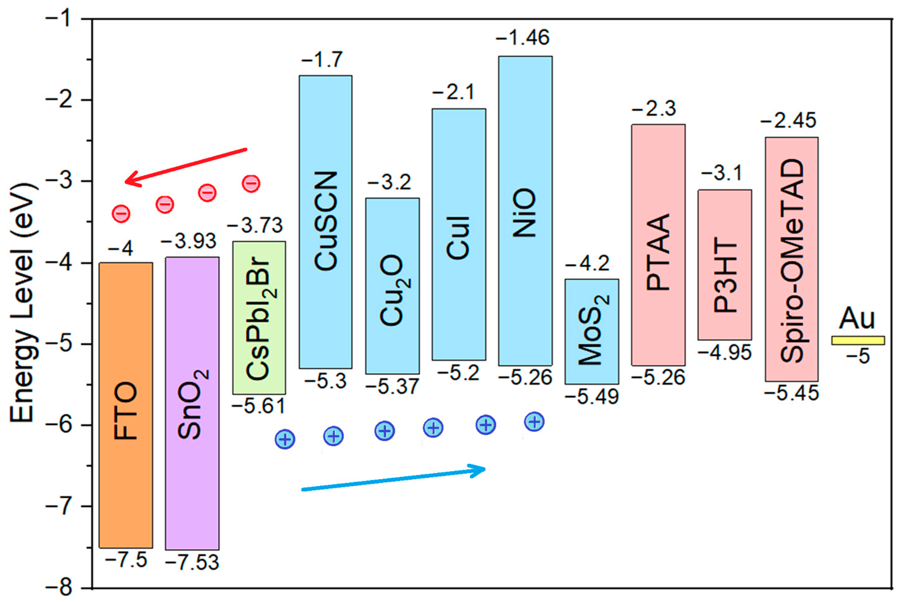
3.1. CsPbI2Br Perovskite Solar Cell Energy Band Diagram and Performance Comparison of Different HTLs

Figure 2 illustrates the energy band diagram of CsPbI2Br perovskite solar cells, with directional arrows showing the carrier transport mechanisms, revealing the mechanism governing electron–hole transport. As indicated by the arrows, electrons migrate from the absorber layer (CsPbI2Br) toward the electron transport layer (SnO2), while holes move toward the HTL, enabling efficient charge separation. Efficient separation and transport of carriers are critical for enhancing photoelectric conversion efficiency. Electrons migrate from the absorber layer (CsPbI2Br) toward the electron transport layer (SnO2), while holes move toward the HTL. For optimal carrier transport, the conduction band minimum (CBM) of the absorber layer must exceed that of the electron transport layer, and the valence band maximum (VBM) of the absorber layer must exceed that of the hole transport layer. This energy band alignment promotes effective carrier separation while reducing recombination losses, thereby enhancing overall solar cell performance.
The performance of eight different HTL materials in the FTO/SnO2/CsPbI2Br/HTL/Au structure under indoor low-light conditions (0.661 mW/cm2) is summarized in Table 4. CuI demonstrated superior performance, achieving a Voc of 1.22 V, FF of 83.84%, Jsc of 0.153 mA/cm2, and PCE of 23.66%. Other materials exhibited PCE values between 21.34% and 22.21%. The superior performance of CuI over materials with significantly higher mobility reveals the fundamental physics governing indoor photovoltaics. Despite MoS2 featuring a 3.4× higher hole mobility (150 vs. 43.9 cm2/V·s), CuI achieves a 9.7% higher PCE. This apparent contradiction is explained through detailed energy band analysis: CuI’s electron affinity (2.1 eV) creates optimal alignment with CsPbI2Br (3.73 eV), establishing a favorable 1.63 eV offset that facilitates efficient hole injection. Conversely, MoS2’s higher electron affinity (4.2 eV) creates energy barriers that limit carrier extraction efficiency despite superior mobility. This finding establishes a new design principle: under low-light conditions where carrier generation rates are fundamentally limited, optimal energy band alignment becomes more critical than carrier mobility. This contrasts sharply with outdoor photovoltaics where high mobility typically dominates performance metrics. Among organic materials, PTAA achieved the highest efficiency (22.05%) with a comparable hole mobility (40 cm2/V·s) to CuI, but its less favorable energy band alignment and inherently lower fill factor limited overall performance compared to the optimally aligned CuI.
To investigate performance under varying illumination intensities, simulations were conducted at two additional white LED light sources: 1000 lux (0.384 mW/cm2) and 200 lux (0.0661 mW/cm2). The results are presented in Table 5 and Table 6. With decreasing light intensity, all efficiency parameters declined correspondingly, with Jsc showing the most significant reduction. At 0.384 mW/cm2, PCE values ranged between 21.14% and 22.57%, with CuI maintaining superior performance. At 0.0661 mW/cm2, PCE decreased to 19.51–20.33%, with P3HT performing marginally better than other materials. To determine the threshold light intensity affecting PCE, simulations were conducted across power densities from 0 to 1 mW/cm2 (Figure 3). Even at extremely low intensities, PCE remained above 19%, with CuI consistently exhibiting optimal performance at medium to high power densities. Based on these findings, CuI was selected for further parameter optimization.
Figure 4 displays the external quantum efficiency (EQE) curve of CsPbI2Br perovskite solar cells, revealing optimal photoelectric conversion in the 350–650 nm wavelength range. This spectral response aligns precisely with the primary emission spectrum of indoor LED light sources, explaining why CsPbI2Br solar cells perform better under indoor illumination than the standard AM 1.5G solar spectrum. Simulation using the AM 1.5G spectrum showed a significant PCE decrease from 23.66% to 17.47%. These findings align with recent literature—Pinzón et al. [5] demonstrated that CuI forms an optimal band alignment with CsPbI2Br, while Guo et al. [10] confirmed that CsPbI2Br solar cells achieve substantially higher efficiencies under indoor lighting (up to 34.2%) compared to standard sunlight conditions (17–19%).

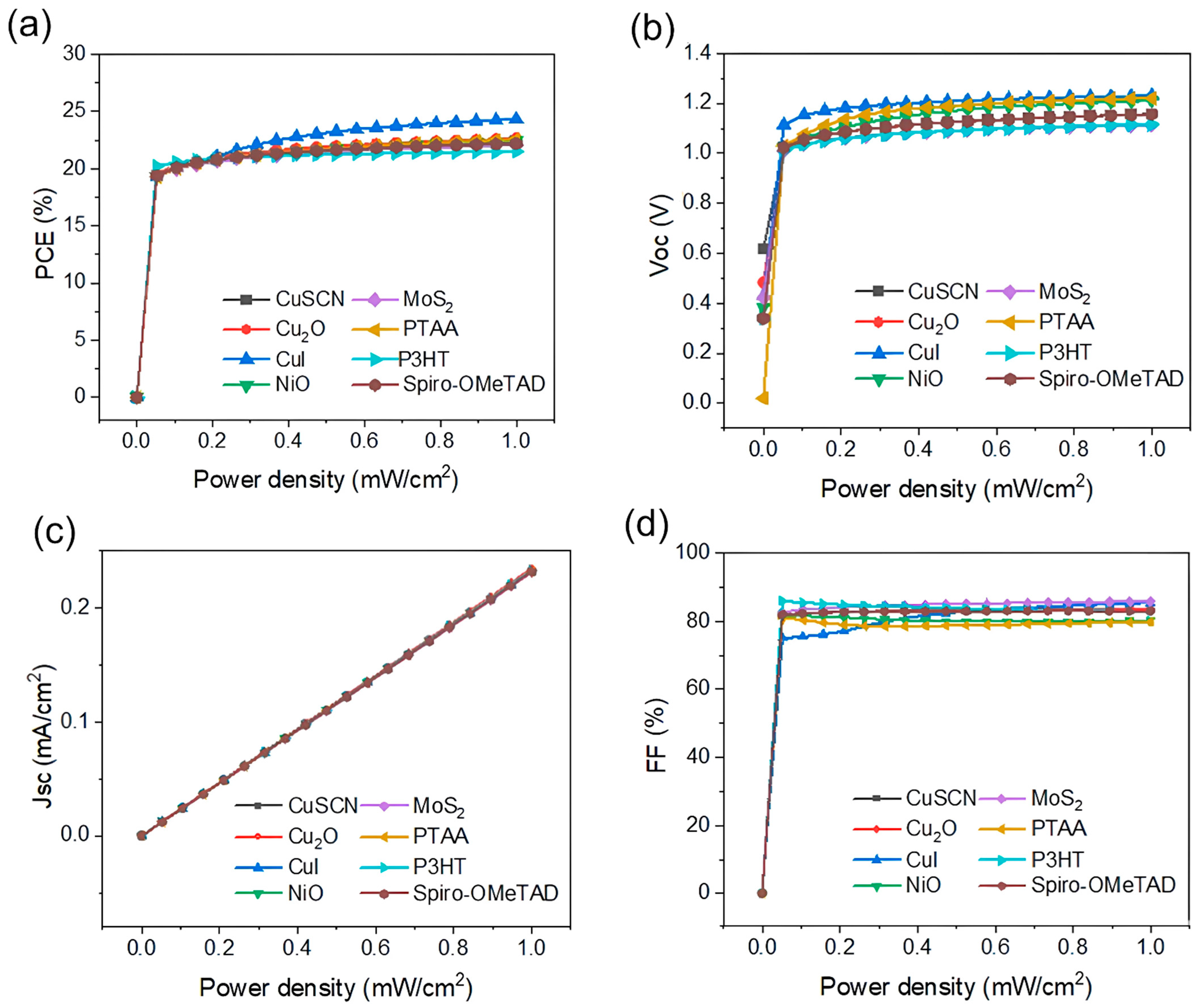
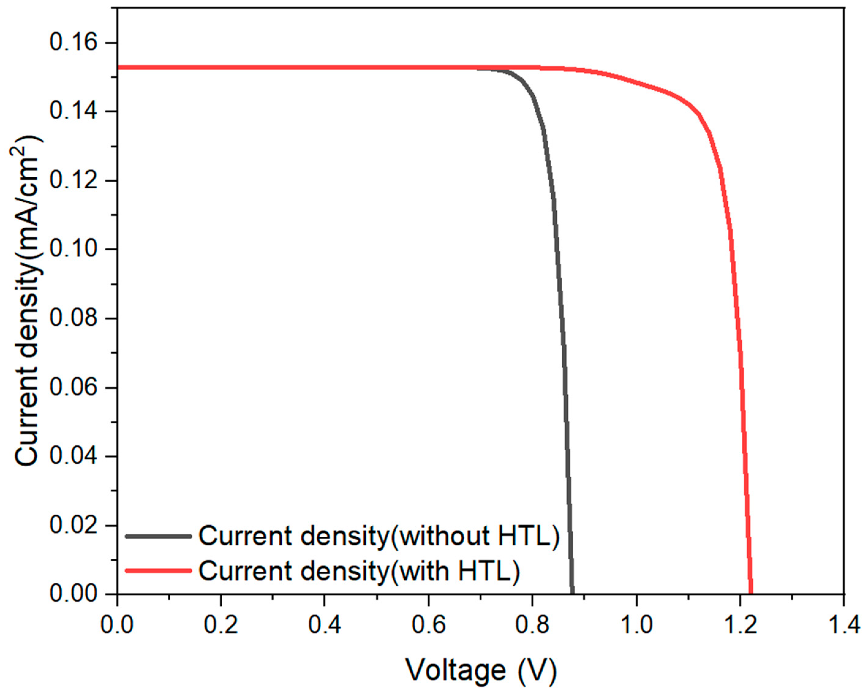
3.2. Performance Parameter Optimization and Structure Analysis of CsPbI2Br Solar Cells

After identifying CuI as the optimal HTL material, we systematically investigated the key parameters affecting device performance. Figure 5 demonstrates the comprehensive effect of various parameters on solar cell performance through a multi-panel analysis combining five critical optimization studies. Figure 5a reveals a remarkable finding: HTL thickness can be reduced to just 0.04 μm without compromising device performance. Once the thickness exceeds 0.04 μm, PCE changes become virtually negligible, suggesting that this minimal thickness is already sufficient for complete hole extraction and transport under low-light conditions. This discovery has profound implications for manufacturing economics, potentially reducing HTL material costs by 80% while maintaining >99% of maximum efficiency. This behavior may indicate either that 0.04 μm provides adequate hole collection efficiency under these low-light conditions or potential limitations in SCAPS-1D’s handling of ultra-thin layer physics, including quantum effects and tunneling mechanisms that become significant at such scales. The physical basis for this behavior lies in the reduced carrier generation rates under low-light conditions. With lower hole densities requiring extraction, thinner HTL layers can adequately transport the photogenerated carriers without introducing significant resistance losses. Nevertheless, this finding suggests that HTL thickness can be reduced to 0.04 μm without compromising performance, offering significant advantages in reducing material costs and simplifying fabrication processes. Future experimental validation would be valuable to confirm these simulation predictions for ultra-thin HTLs. Figure 5b shows that as CsPbI2Br absorber layer thickness increases from 0.2 μm to approximately 1 μm, PCE gradually improves and stabilizes. Beyond 1.2 μm, PCE decreases due to increased carrier recombination and series resistance. Additionally, thicker absorber layers typically exhibit higher defect densities. Based on these findings, the optimal configuration includes an HTL thickness of 0.04 μm and absorber layer thickness of 1 μm, enhancing PCE to 26.3%.
Figure 5c analyzes the influence of CuI’s shallow acceptor density on device performance. When the concentration exceeds 1017 cm−3, PCE begins to decline, decreasing by approximately 3% at 1019 cm−3. Excessive doping can disrupt energy band alignment, increase recombination rates, or create rough interfaces that increase leakage current. Therefore, the optimal doping concentration ranges between 1015 and 1017 cm−3. As shown in Figure 5d, the absorber layer’s defect concentration has a more pronounced effect on PCE. When defect concentration exceeds 1015 cm−3, PCE drops dramatically, with potential decreases of up to 8%. Additionally, Figure 5e demonstrates that the interface defect concentration between the absorber layer and HTL significantly impacts performance. Once the interface defect concentration exceeds 1012 cm−3, PCE noticeably decreases by up to 4%. Such high interface defect concentrations can originate from several sources including lattice mismatch between CsPbI2Br and HTL materials, poor processing conditions during interface formation, surface contamination, inadequate interface cleaning procedures, or suboptimal deposition parameters that fail to achieve proper atomic-scale contact between layers, highlighting the importance of interface engineering for high-efficiency devices.
Under optimized conditions—HTL thickness of 0.04 μm, absorber layer thickness of 0.87 μm, HTL doping concentration of 1017 cm−3, absorber layer defect concentration of 1015 cm−3, and interface defect concentration of 109 cm−3—CsPbI2Br solar cells under indoor low-light conditions achieved a PCE of 28.57%, with a Voc of 1.2468 V, Jsc of 0.17043 mA/cm2, and FF of 88.90%. To evaluate the necessity of an HTL, we simulated an HTL-free structure (FTO/SnO2/CsPbI2Br/Au), which yielded a PCE of 17.6%, Voc of 0.8759 V, Jsc of 0.15306 mA/cm2, and FF of 86.81%—6% less efficient than the CuI-HTL structure. Figure 6 compares the J-V curves of both structures, revealing that the open-circuit voltage of the HTL-free structure is approximately 28% lower than the CuI-HTL structure (0.8759 V vs. 1.22 V). This substantial difference indicates that the HTL layer significantly contributes to overall device performance through multiple physical mechanisms: (1) the HTL creates optimal band bending at the perovskite/electrode interface, establishing a built-in electric field that facilitates hole collection; (2) it reduces interface recombination by providing proper energy level alignment and passivating surface states; (3) the HTL prevents electron leakage toward the anode, ensuring unidirectional carrier flow; and (4) it enhances hole collection efficiency by providing a low-resistance pathway for hole transport to the metal contact. These combined effects result in the observed 28% improvement in open-circuit voltage and overall enhanced device performance.

3.3. Literature Comparison

To verify the reliability of our simulation results, we compared our optimized CsPbI2Br perovskite solar cell structure with recent experimental findings (Table 7 and Table 8). While simulation-only studies have inherent limitations in capturing all real-world device physics and fabrication-related variations, our results show good agreement with the experimental literature, providing confidence in our theoretical predictions. Under a standard AM 1.5G solar spectrum, our optimized FTO/SnO2/CsPbI2Br/CuI/Au structure achieved a simulated PCE of 19.48%, Voc of 1.376 V, Jsc of 16.35 mA/cm2, and FF of 86.57%—all exceeding the parameters reported in the literature for similar structures. Compared to the FTO/TiO2/CsPbI2Br/MoO2-PTAA/Carbon structure reported by Lee et al. [23] (PCE of 14.67%), our simulated structure shows an approximately 33% higher efficiency. Similarly, compared to the structure using Spiro-OMeTAD as the HTL reported by Chen et al. [24] (PCE of 15.03%), our structure demonstrates an approximately 30% higher efficiency. This performance difference can be attributed to several factors: (1) CuI forms a more ideal energy band alignment with CsPbI2Br, facilitating efficient charge separation; (2) our systematic optimization of the interface defect concentration reduced recombination losses; and (3) the optimized layer thickness configuration balances light absorption and charge transport requirements. The disparity between the simulation and experimental results can be partially attributed to practical fabrication challenges such as film uniformity, interface roughness, and environmental factors that are not accounted for in simulations.
Future experimental validation should focus on (1) fabricating CuI-based HTL devices using the optimized parameters identified in this study, (2) characterizing interface quality through advanced spectroscopic techniques, (3) measuring device performance under controlled indoor LED illumination conditions, and (4) investigating long-term stability under realistic indoor operating environments. Such experimental work would provide crucial validation of our theoretical predictions and enable practical device optimization.
Notably, our optimized solar cells exhibit a significantly higher PCE (28.57%) under indoor low-light conditions (0.661 mW/cm2) than under the standard AM 1.5G solar spectrum (19.48%). While the short-circuit current density under indoor conditions (0.17043 mA/cm2) is far lower than under standard illumination (16.35 mA/cm2), this is explained by the PCE calculation formula:
PCE = (Voc × Jsc × FF)/Pin
Given that the indoor power density (0.661 mW/cm2) is only about 0.661% of the standard AM 1.5G (100 mW/cm2), the ratio of short-circuit current densities (approximately 1:96) is consistent with the ratio of light source power densities (approximately 1:151). Under low-light conditions, despite a significantly lower short-circuit current density, the relatively high open-circuit voltage and fill factor, combined with the substantially lower denominator in Equation (4), result in a higher calculated PCE.
More significantly, the bandgap of CsPbI2Br (1.88 eV) is particularly well-suited for indoor low-light spectral distribution. As shown in Figure 4, this material exhibits optimal photoelectric conversion in the 350–650 nm range, corresponding closely to the emission spectrum of indoor LED light sources. In contrast, the standard AM 1.5G solar spectrum contains significant long-wavelength components that CsPbI2Br cannot effectively absorb. Compared to the literature, the indoor low-light PCE of our optimized structure (28.57%) exceeds the 23.51% reported by Kim et al. [25] and the 23.24% reported by Bahadur et al. [26], further confirming the theoretical advantages of CuI as an HTL material in CsPbI2Br perovskite solar cells for indoor applications.
Table 7. Comparison of simulated optimized CsPbI2Br perovskite solar cell performance with recent experimental results under the standard AM 1.5G solar spectrum (100 mW/cm2).
Device StructureVoc (V)Jsc (mA/cm2)FF (%)PCE (%)Reference
FTO/SnO2/CsPbI2Br/CuI/Au1.37616.3586.5719.48This work
ITO/ZnO/CsPbI2Br/P3HT/Au1.22014.8875.7013.74Bahadur [8]
ITO/NiOx/CsPbI2Br/PC61BM/BCP/Ag1.1015.7575.1313.01Chen [27]
FTO/TiO2/CsPbI2Br/MoO2-PTAA/Carbon1.2115.0780.4414.67Lee [23]
FTO/TiO2/CsPbI2Br/Carbon1.1513.876410.21Dong [28]
FTO/TiO2/CsPbI2Br/Spiro-OMeTAD/Au1.2115.678015.03Chen [24]
Table 8. Comparison of simulated optimized CsPbI2Br perovskite solar cell performance with recent experimental results under indoor white LED illumination.
Device Structure
(Illumination Intensity)
Voc (V)Jsc (mA/cm2)FF (%)PCE (%)Reference
FTO/SnO2/CsPbI2Br/CuI/Au
(0.661mW/cm2)
1.24680.1704388.9028.57This work
ITO/SnO2/ZnO/CsPbI2Br/P3HT/Au
(0.382 mW/cm2)
1.0510.11076.7923.24Bahadur [26]
ITO/SnO2/CsPbI2Br/Spiro-OMeTAD/Au
(0.3098 mW/cm2)
0.950.1147023.51Kim [25]

4. Conclusions

This research establishes new theoretical foundations for indoor perovskite photovoltaics through several key contributions. First, we demonstrate that an optimal energy band alignment supersedes carrier mobility under low-light conditions, challenging conventional photovoltaic design paradigms. The superior performance of CuI over MoS2 (despite 3.4× lower mobility) reveals that energy band alignment becomes the dominant factor in indoor applications. Second, the identification of ultra-thin HTL requirements (0.04 μm) represents a breakthrough for cost-effective manufacturing, potentially reducing material costs by 80% compared to conventional 0.2 μm layers while maintaining >99% of maximum efficiency. This discovery provides a clear pathway to economical indoor photovoltaic production. This research utilized SCAPS-1D simulation software to investigate the impact of various HTLs on the PCE of CsPbI2Br perovskite solar cells under indoor low-light conditions (white LED, 560 lux, 0.661 mW/cm2). The study compared eight HTL materials (CuSCN, Cu2O, CuI, NiO, MoS2, PTAA, P3HT, and Spiro-OMeTAD) across varying light intensities (0–1 mW/cm2). The results demonstrated that CuI exhibited superior energy level compatibility with the absorber layer and the highest PCE of 23.66%, attributed to its optimal band alignment and high hole mobility. CuI also demonstrated better stability and a higher PCE compared to other materials across most low-light intensity ranges. Parameter optimization revealed that HTL thickness has minimal impact on efficiency and can be reduced to 0.04 μm, while absorber layer thickness, defect concentration, and interface defect density significantly influenced performance. Under optimized conditions (absorber layer: 0.87 μm; defect concentration: 1015 cm−3; interface defect concentration: 109 cm−3), the PCE increased to 28.57% with a Voc of 1.2468 V, Jsc of 0.17043 mA/cm2, and FF of 88.90%. The HTL-free structure showed a reduced efficiency (17.6%) and open-circuit voltage (0.8759 V), confirming HTL’s crucial role in device performance. This study establishes fundamental design principles showing that material selection criteria differ fundamentally from outdoor applications. The validated theoretical framework provides rational guidelines for next-generation IoT energy harvesting devices. The findings highlight CsPbI2Br perovskite solar cells’ potential for powering low-power electronics in indoor environments where conventional solar cells perform poorly. Future research should focus on experimental validation of the ultra-thin HTL concept and scaling of the optimized device architecture for commercial applications.

Author Contributions

C.-H.P.: Methodology, Formal analysis, Writing—original draft; Y.-C.L.: Conceptualization, Resources, Writing—review and editing. All authors have read and agreed to the published version of the manuscript.

Funding

This research was funded by National Science and Technology Council under grant number the National Science and Technology Council under grant number 113-2221-E-018-001.

Institutional Review Board Statement

The authors declare that this research was conducted in accordance with ethical standards. No human or animal subjects were involved in this study. All computational methods and data analysis procedures followed established scientific practices.

Data Availability Statement

The computational data and simulation parameters used in this study are available from the corresponding author upon reasonable request. The SCAPS-1D software (version 3.3.11) used for the simulations is freely available from the University of Gent. All other data generated or analyzed during this study are included in this published article.

Acknowledgments

The authors wish to thank the developers of SCAPS at the University of Gent for making their software package publicly available free of charge.

Conflicts of Interest

The authors declare that they have no known competing financial interests or personal relationships that could have appeared to influence the work reported in this paper.

References

  1. Alanazi, T.I.; Shaker, A.; Zein, W. Design and Simulation of 2D Ruddlesden-Popper Perovskite Solar Cells under LED Illumination: Role of ETL and Front Contact Band Alignment. Sol. Energy Mater. Sol. Cells 2024, 274, 112992. [Google Scholar] [CrossRef]
  2. Wu, M.; Kuo, C.; Jhuang, L.; Chen, P.; Lai, Y.; Chen, F. Bandgap engineering enhances the performance of mixed-cation perovskite materials for indoor photovoltaic applications. Adv. Energy Mater. 2019, 9, 1901863. [Google Scholar] [CrossRef]
  3. Yang, M.; Kim, D.; Park, Y. High-efficiency perovskite solar cells for indoor photovoltaic applications: Recent progress and challenges. Energy Environ. Sci. 2021, 14, 643–654. [Google Scholar] [CrossRef]
  4. Zhang, L.; Wang, J.; Liu, T. Spectral response optimization of perovskite photovoltaics for indoor light harvesting. Adv. Energy Mater. 2021, 11, 2100332. [Google Scholar]
  5. Pinzón, C.; Martínez, N.; Casas, G.; Alvira, F.C.; Denon, N.; Brusasco, G.; Chanduví, H.M.; Gil Rebaza, A.V.; Cappelletti, M.A. Optimization of Inverted All-Inorganic CsPbI3 and CsPbI2Br Perovskite Solar Cells by SCAPS-1D Simulation. Solar 2022, 2, 559–571. [Google Scholar] [CrossRef]
  6. Wang, R.; Xue, J.; Wang, K.L. Phase stability engineering of CsPbI2Br perovskites for photovoltaic applications. J. Phys. Chem. Lett. 2021, 12, 1465–1472. [Google Scholar]
  7. Huang, S.; Zhang, B.; Wu, Y. Comparative study of all-inorganic cesium lead halide perovskites for indoor photovoltaic ap-plications. ACS Appl. Mater. Interfaces 2021, 13, 43833–43841. [Google Scholar]
  8. Bahadur, J.; Cho, S.; Pandey, P.; Yoon, S.; Lee, D.-G.; Ryu, J.; Meena, V.; Kang, D.-W. Fully hot Air-Processed All-Inorganic CsPbI2Br perovskite solar cells for outdoor and indoor applications. Appl. Surf. Sci. 2025, 684, 161909. [Google Scholar] [CrossRef]
  9. Liu, Y.; Lang, K.; Han, H.; Liu, H.; Fu, Y.; Zou, P.; Lyu, Y.; Xu, J.; Yao, J. Crystallization management of CsPbI2Br perovskites by PbAc2-incorporated twice spin-coating process for efficient and stable CsPbI2Br perovskite solar cells. J. Energy Chem. 2024, 97, 419–428. [Google Scholar] [CrossRef]
  10. Guo, Z.; Jena, A.K.; Takei, I.; Ikegami, M.; Ishii, A.; Numata, Y.; Miyasaka, T. Dopant-free polymer HTM-based CsPbI2Br solar cells with efficiency over 17% in sunlight and 34% in indoor light. Adv. Funct. Mater. 2021, 31, 2103614. [Google Scholar] [CrossRef]
  11. Wang, K.-L.; Zhou, Y.-H.; Lou, Y.-H.; Wang, Z.-K. Perovskite indoor photovoltaics: Opportunity and challenges. Chem. Sci. 2021, 12, 11936–11954. [Google Scholar] [CrossRef] [PubMed]
  12. Huy, V.P.H.; Nguyen, T.M.H.; Bark, C.W. Recent Advances of Doped SnO2 as Electron Transport Layer for High-Performance Perovskite Solar Cells. Materials 2023, 16, 6170. [Google Scholar] [CrossRef]
  13. Dong, Y.; Duan, J.; Luo, D.; Liu, J.; Wang, X.; Liu, X.; Huang, Z.; Li, X.; Gao, Y. Interface optimization of CsPbI2Br based perovskite solar cells by device simulation. Mater. Today Commun. 2024, 39, 108695. [Google Scholar] [CrossRef]
  14. Li, N.; Niu, X.; Ding, L. Emerging dopant-free hole transport materials for perovskite solar cells. Energy Environ. Sci. 2020, 13, 3608–3620. [Google Scholar]
  15. Kim, H.; Zhao, J.; Du, M. Long-term stable inorganic hole transport layers for efficient perovskite solar cells. Adv. Funct. Mater. 2020, 30, 2002674. [Google Scholar]
  16. Lopez-Varo, P.; Jiménez-Tejada, J.A.; García-Rosell, M.; Ravishankar, S.; Garcia-Belmonte, G.; Bisquert, J.; Almora, O. Device Physics of Hybrid Perovskite Solar cells: Theory and Experiment. Adv. Energy Mater. 2018, 8, 1702772. [Google Scholar] [CrossRef]
  17. Xing, G.; Wu, Y.; Li, X. Multi-scale simulation approaches for perovskite photovoltaics: From material properties to device performance. J. Mater. Chem. A 2021, 9, 17545–17570. [Google Scholar]
  18. Khatoon, S.; Chakraborty, V.; Yadav, S.K.; Diwakar, S.; Singh, J.; Singh, R.B. Simulation study of CsPbIxBr1-x and MAPbI3 heterojunction solar cell using SCAPS-1D. Sol. Energy 2023, 254, 137–157. [Google Scholar] [CrossRef]
  19. Basak, A.; Singh, U.P. Numerical modelling and analysis of earth abundant Sb2S3 and Sb2Se3 based solar cells using SCAPS-1D. Sol. Energy Mater. Sol. Cells 2021, 230, 111184. [Google Scholar] [CrossRef]
  20. Siddique, M.; Sultan, M.; Safeer, S.H. Device Optimization of CsPbI2Br-based Inorganic Perovskite Solar Cells using Different Hole and Electron Transport Layers via SCAPS-1D. Next Mater. 2025, 8, 100532. [Google Scholar] [CrossRef]
  21. Sharma, D.; Mehra, R.; Raj, B. Comparative study of hole transporting layers commonly used in high-efficiency perovskite solar cells. J. Mater. Sci. 2022, 57, 21172–21191. [Google Scholar] [CrossRef]
  22. Raoui, Y.; Ez-Zahraouy, H.; Ahmad, S.; Kazim, S. Unravelling the theoretical window to fabricate high performance inorganic perovskite solar cells. Sustain. Energy Fuels 2021, 5, 219–229. [Google Scholar] [CrossRef]
  23. Lee, D.S.; Ki, M.J.; Lee, H.J.; Park, J.K.; Hong, S.Y.; Kim, B.W.; Heo, J.H.; Im, S.H. Fully Scalable and Stable CsPbI2Br Solar Cells Realized by an All-Spray-Coating Process. ACS Appl. Mater. Interfaces 2022, 14, 7926–7935. [Google Scholar] [CrossRef] [PubMed]
  24. Chen, H.; Ma, Y.; Wang, X.; Yao, G.; Du, Y.; Zhou, J.; Zhu, L.; Zhao, X.; Yang, S.; Liu, X.; et al. Improving the stability and efficiency of inorganic CsPbI2Br perovskite via surface reconstruction strategy. Chem. Eng. J. 2022, 442, 136242. [Google Scholar] [CrossRef]
  25. Kim, K.S.; Jin, I.S.; Park, S.H.; Lim, S.J.; Jung, J.W. Methylammonium Iodide-Mediated Controlled Crystal Growth of CsPbI2Br Films for Efficient and Stable All-Inorganic Perovskite Solar Cells. ACS Appl. Mater. Interfaces 2020, 12, 36228–36236. [Google Scholar] [CrossRef]
  26. Bahadur, J.; Cho, S.; Pandey, P.; Ryu, J.; Yoon, S.; Lee, D.-G.; Song, J.T.; Cho, J.S.; Kang, D.-W. Surface defect passivation of All-Inorganic CsPbI2Br perovskites via fluorinated ionic liquid for efficient Outdoor/Indoor photovoltaics processed in ambient air. Appl. Surf. Sci. 2023, 637, 157901. [Google Scholar] [CrossRef]
  27. Chen, Y.; Liu, J.; Wu, Y.; Wang, Z.; Li, J.; Liu, X.; Yang, D.; Wang, X. Performance enhancement of inverted CsPbI2Br perovskite solar cells via butylammonium cation additive modification. Mater. Lett. 2025, 379, 137643. [Google Scholar] [CrossRef]
  28. Dong, C.; Han, X.; Li, W.; Qiu, Q.; Wang, J. Anti-solvent assisted multi-step deposition for efficient and stable carbon-based CsPbI2Br all-inorganic perovskite solar cell. Nano Energy 2019, 59, 553–559. [Google Scholar] [CrossRef]
Figure 1. Schematic diagram of the proposed perovskite solar cell structures: (a) without HTL configuration; (b) with HTL configuration.
Solids 06 00031 g001
Figure 2. Energy band diagram of CsPbI2Br perovskite solar cells showing electron and hole transport mechanisms.
Solids 06 00031 g002
Figure 3. Performance parameters of CsPbI2Br perovskite solar cells with different HTLs as a function of light intensity: (a) PCE; (b) Voc; (c) Jsc; and (d) FF.
Solids 06 00031 g003
Figure 4. EQE spectrum of CsPbI2Br perovskite solar cells with CuI as the HTL.
Solids 06 00031 g004
Figure 5. Effect of (a) HTL (CuI) thickness, (b) absorber layer thickness, (c) CuI’s shallow acceptor density, (d) absorber layer defect concentration, and (e) interface defect concentration between the absorber layer and HTL on solar cell performance parameters PCE, Voc, Jsc, and FF.
Solids 06 00031 g005
Figure 6. J-V characteristics of CsPbI2Br perovskite solar cells with and without HTL under indoor low-light conditions.
Solids 06 00031 g006
Table 1. Material parameters for the primary structural layers used in the SCAPS-1D simulation [5,20,21].
ParametersFTOSnO2CsPbI2Br
Thickness (μm)0.20.20.5
Bandgap (eV)3.53.61.88
Relative permittivity998.6
Electron affinity (eV)43.933.73
Effective DoS at CB (cm−3)2.2 × 10183.16 × 10181.9 × 1018
Effective DoS at VB (cm−3)1.8 × 10192.5 × 10192.370 × 1019
Mob. of electrons (cm2/V·s)2020200
Mob. of holes (cm2/V·s)1010200
Dop. conc. of acceptor (cm−3)000
Dop. conc. of donor (cm−3)2.0 × 10181.0× 10181.0 × 1015
Defect density (cm−3)1.0 × 10151.0 × 10153.64 × 1015
Table 2. Physical and electronic properties of various hole transport materials (HTMs) investigated in this study [5,20,21,22].
ParametersCuSCNCu2OCuINiOMoS2PTAAP3HTSpiro-OMeTAD
Thickness (μm)0.20.20.20.20.20.20.20.2
Bandgap (eV)3.62.173.13.81.292.961.853
Relative permittivity107.16.53.84.2693.43
Electron affinity (eV)1.73.22.11.464.22.33.12.45
Effective DoS at CB (cm−3)2.29 × 10192 × 10172.8 × 10192.8 × 10192.2 × 10182 × 10182 × 10202.2 × 1018
Effective DoS at VB (cm−3)1.8 × 10181.1 × 10191 × 10191 × 10191.8 × 10191 × 10192 × 10201.9 × 1019
Mob. of electrons (cm2/V·s)1002001001210011 × 10−42 × 10−4
Mob. of holes (cm2/V·s)258043.93.8150401 × 10−32 × 10−4
Dop. conc. of acceptor (cm−3)1 × 10181 × 10181 × 10181 × 10181 × 10181 × 10181 × 10181 × 1018
Defect density (cm−3)1 × 10151 × 10151 × 10151 × 10151 × 10151 × 10151 × 10151 × 1015
Table 3. Interface defect parameters implemented in the SCAPS-1D simulation model [20].
ParametersSnO2/CsPbI2BrCsPbI2Br/CuI
Defect typesNeutralNeutral
Capture cross section electrons (cm2)1.0 × 10−191.0 × 10⁻¹⁹
Capture cross section holes (eV)1.0 × 10−191.0 × 10⁻¹⁹
Energy distributionsSingleSingle
Ref for defect energy levelAbove the highest EvAbove the highest Ev
Energy with respect to reference (eV)0.60.6
Total density (cm−3)1.0 × 1091.0 × 109
Table 4. Performance metrics of CsPbI2Br perovskite solar cells with various HTLs under indoor low-light conditions (white LED, 0.661 mW/cm2).
HTLs/PerformancesVoc (V)Jsc (mA/cm2)FF (%)PCE (%)
CuSCN1.13810.15383.3521.96
Cu2O1.13790.15483.4322.21
CuI1.21910.15383.8423.66
NiO1.18910.15379.8521.98
MoS21.09080.15285.6321.57
PTAA1.20440.15379.0422.05
P3HT1.10160.15383.3921.34
Spiro-OMeTAD1.13790.15382.9121.84
Table 5. Performance metrics of CsPbI2Br perovskite solar cells with various HTLs under reduced indoor illumination (white LED, 0.384 mW/cm2).
HTLs/PerformancesVoc (V)Jsc (mA/cm2)FF (%)PCE (%)
CuSCN1.11310.088983.0421.4
Cu2O1.11320.089883.1221.64
CuI1.2020.088981.122.57
NiO1.15210.088980.221.39
MoS21.08250.088784.7521.19
PTAA1.17840.088978.5221.43
P3HT1.08170.089284.1221.14
Spiro-OMeTAD1.11360.088982.8221.35
Table 6. Performance metrics of CsPbI2Br perovskite solar cells with various HTLs under reduced indoor illumination (white LED, 0.0661 mW/cm2).
HTLs/PerformancesVoc (V)Jsc (mA/cm2)FF (%)PCE (%)
CuSCN1.03130.015382.0119.58
Cu2O1.03210.015482.0519.81
CuI1.12820.015374.9919.59
NiO1.03620.015381.4319.54
MoS21.01970.015282.8419.51
PTAA1.04330.015380.8819.54
P3HT1.02020.015385.7520.33
Spiro-OMeTAD1.03330.015382.0519.63
Disclaimer/Publisher’s Note: The statements, opinions and data contained in all publications are solely those of the individual author(s) and contributor(s) and not of MDPI and/or the editor(s). MDPI and/or the editor(s) disclaim responsibility for any injury to people or property resulting from any ideas, methods, instructions or products referred to in the content.

