
Flow Rate-Driven Morphology Evolution of Chemical Vapor Deposited WS2 at Varying Temperatures


Abstract

1. Introduction
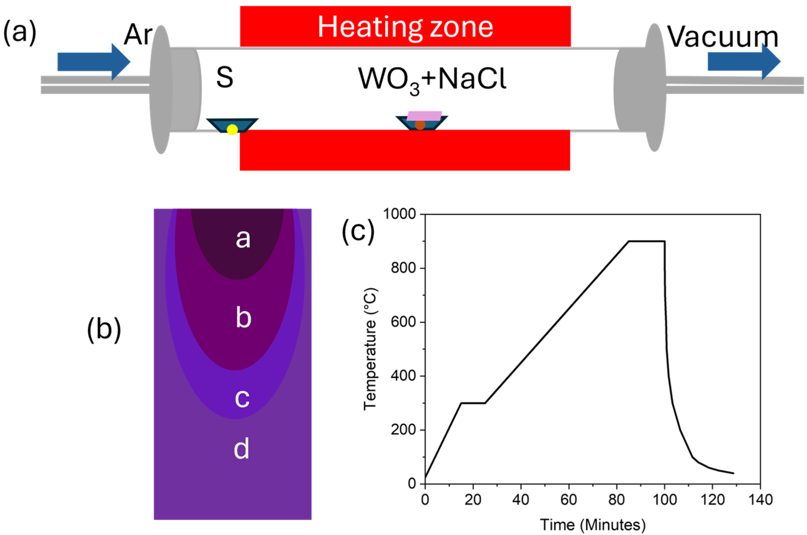
2. Materials and Methods
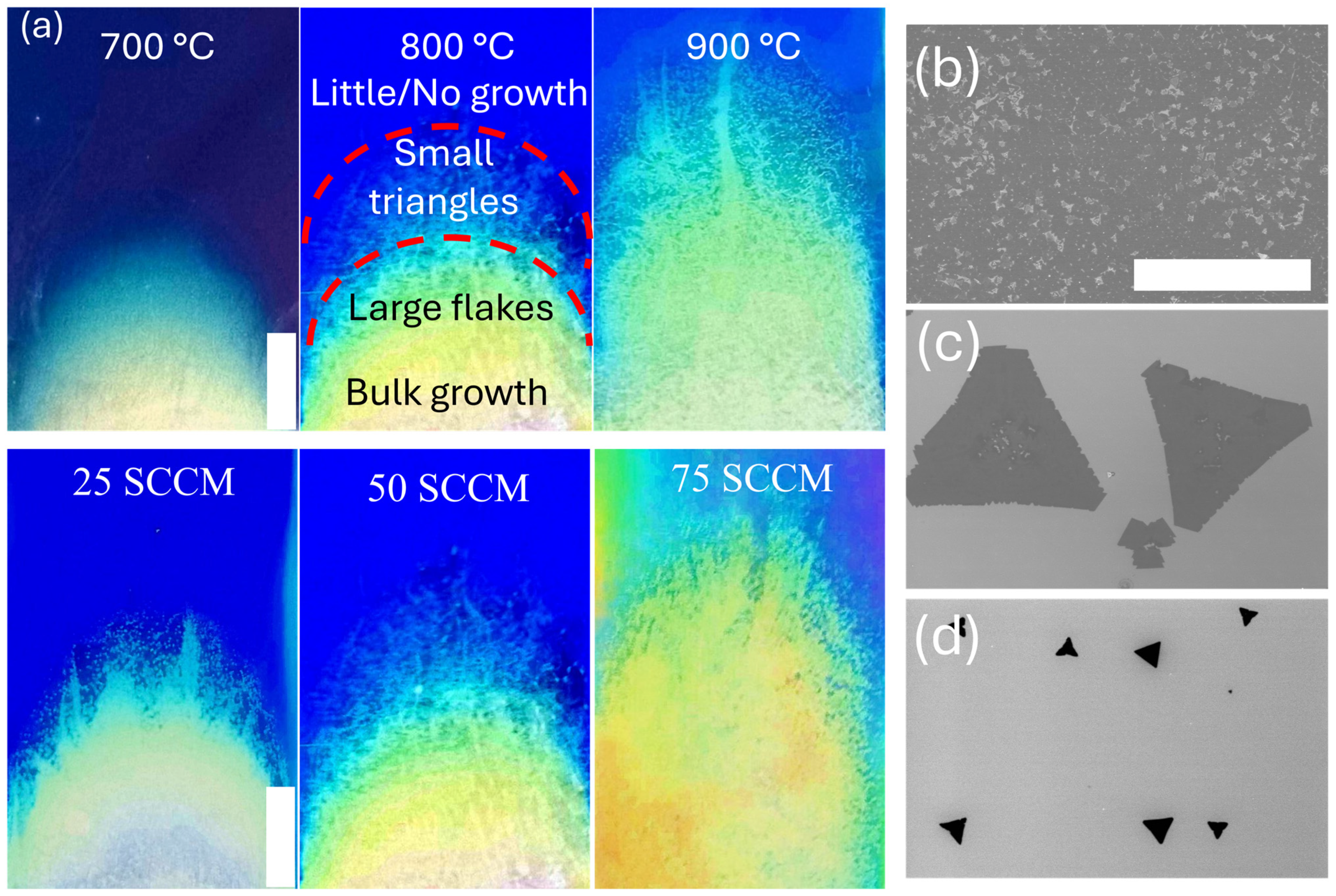
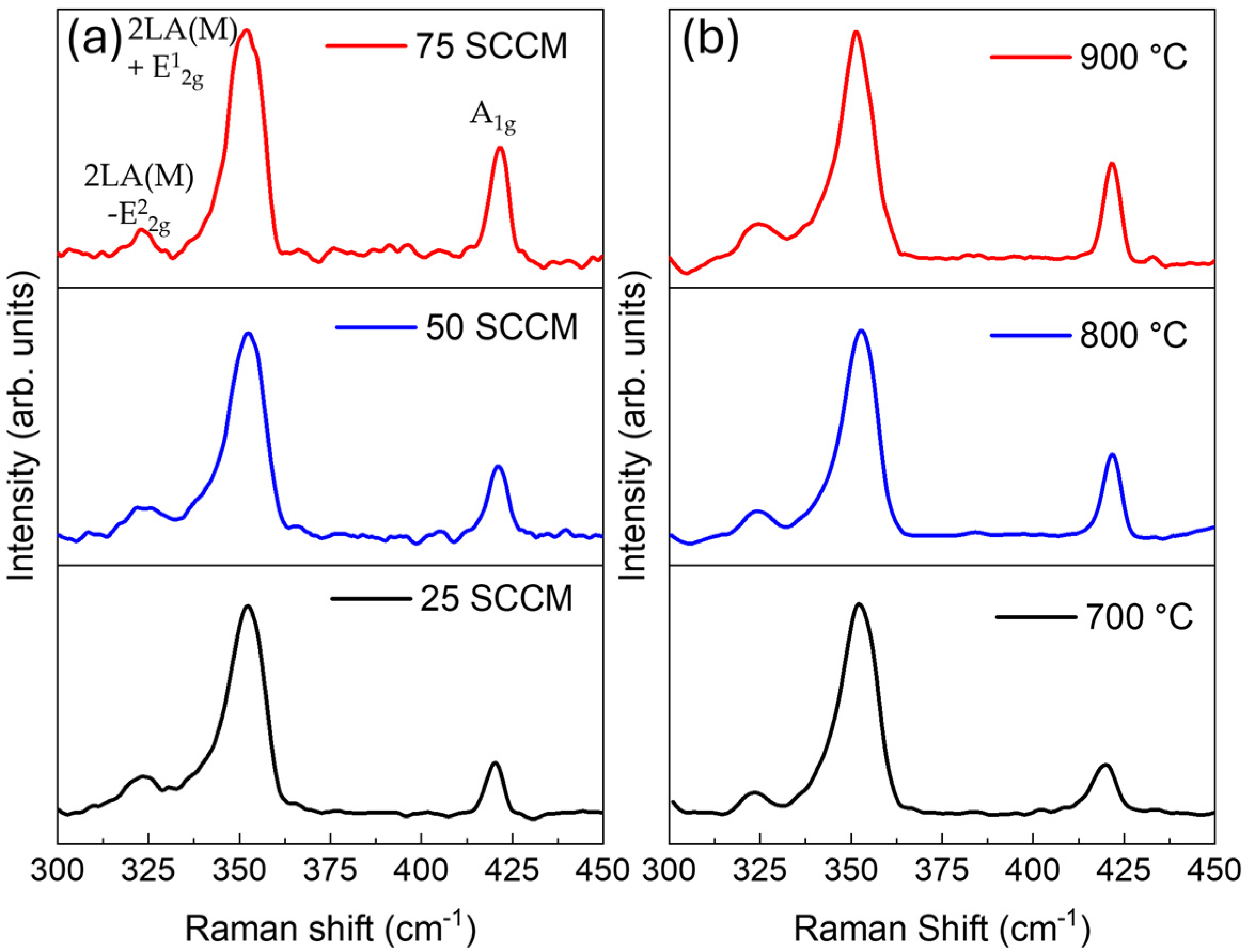
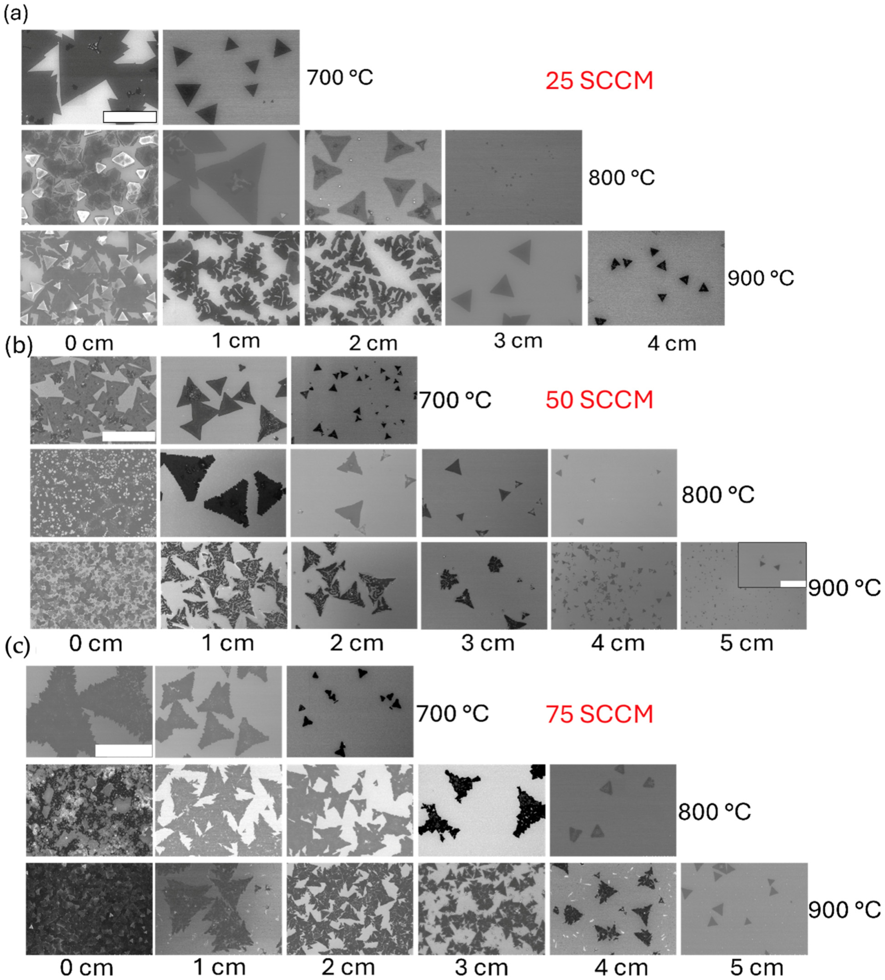
3. Results
4. Discussion
5. Conclusions
Author Contributions
Funding
Data Availability Statement
Acknowledgments
Conflicts of Interest
References
- Ovchinnikov, D.; Allain, A.; Huang, Y.-S.; Dumcenco, D.; Kis, A. Electrical Transport Properties of Single-Layer WS2. ACS Nano 2014, 8, 8174–8181. [Google Scholar] [CrossRef]
- Shi, S.; Liang, S.; Zhu, Z.; Cai, K.; Pollard, S.D.; Wang, Y.; Wang, J.; Wang, Q.; He, P.; Yu, J.; et al. All-electric magnetization switching and Dzyaloshinskii-Moriya interaction in WTe2/ferromagnet heterostructures. Nat. Nanotechnol. 2019, 14, 945–949. [Google Scholar] [CrossRef]
- Xiao, D.; Liu, G.-B.; Feng, W.; Xu, X.; Yao, W. Coupled Spin and Valley Physics in Monolayers of MoS 2 and and Other Group-VI Dichalcogenides. Phys. Rev. Lett. 2012, 108, 196802. [Google Scholar] [CrossRef]
- Zhu, Z.Y.; Cheng, Y.C.; Schwingenschlögl, U. Giant spin-orbit-induced spin splitting in two-dimensional transition-metal dichalcogenide semiconductors. Phys. Rev. B 2011, 84, 153402. [Google Scholar] [CrossRef]
- Wurstbauer, U.; Miller, B.; Parzinger, E.; Holleitner, A.W. Light–matter interaction in transition metal dichalcogenides and their heterostructures. J. Phys. D Appl. Phys. 2017, 50, 173001. [Google Scholar] [CrossRef]
- Cao, J.; Fiore, S.; Klinkert, C.; Vetsch, N.; Luisier, M. Light-matter interactions in van der Waals photodiodes from first principles. Phys. Rev. B 2022, 106, 035306. [Google Scholar] [CrossRef]
- Wang, Q.H.; Kalantar-Zadeh, K.; Kis, A.; Coleman, J.N.; Strano, M.S. Electronics and optoelectronics of two-dimensional transition metal dichalcogenides. Nat. Nanotechnol. 2012, 7, 699–712. [Google Scholar] [CrossRef]
- Zhao, W.; Ghorannevis, Z.; Chu, L.; Toh, M.; Kloc, C.; Tan, P.-H.; Eda, G. Evolution of Electronic Structure in Atomically Thin Sheets of WS2 and WSe2. ACS Nano 2013, 7, 791–797. [Google Scholar] [CrossRef]
- Braga, D.; Lezama, I.G.; Berger, H.; Morpurgo, A.F. Quantitative Determination of the Band Gap of WS2 with Ambipolar Ionic Liquid-Gated Transistors. Nano Lett. 2012, 12, 5218–5223. [Google Scholar] [CrossRef]
- Voiry, D.; Mohite, A.; Chhowalla, M. Phase engineering of transition metal dichalcogenides. Chem. Soc. Rev. 2015, 44, 2702–2712. [Google Scholar] [CrossRef]
- Zeng, H.; Liu, G.-B.; Dai, J.; Yan, Y.; Zhu, B.; He, R.; Xie, L.; Xu, S.; Chen, X.; Yao, W.; et al. Optical signature of symmetry variations and spin-valley coupling in atomically thin tungsten dichalcogenides. Sci. Rep. 2013, 3, 1608. [Google Scholar] [CrossRef]
- Nayak, P.K.; Lin, F.-C.; Yeh, C.-H.; Huang, J.-S.; Chiu, P.-W. Robust room temperature valley polarization in monolayer and bilayer WS2. Nanoscale 2016, 8, 6035–6042. [Google Scholar] [CrossRef]
- Hwang, W.S.; Remskar, M.; Yan, R.; Protasenko, V.; Tahy, K.; Chae, S.D.; Zhao, P.; Konar, A.; Xing, H.; Seabaugh, A.; et al. Transistors with chemically synthesized layered semiconductor WS2 exhibiting 105 room temperature modulation and ambipolar behavior. Appl. Phys. Lett. 2012, 101, 013107. [Google Scholar] [CrossRef]
- Iqbal, M.W.; Iqbal, M.Z.; Khan, M.F.; Shehzad, M.A.; Seo, Y.; Park, J.H.; Hwang, C.; Eom, J. High-mobility and air-stable single-layer WS2 field-effect transistors sandwiched between chemical vapor deposition-grown hexagonal BN films. Sci. Rep. 2015, 5, 10699. [Google Scholar] [CrossRef]
- Bin Rafiq, K.S.; Amin, N.; Alharbi, H.F.; Luqman, M.; Ayob, A.; Alharthi, Y.S.; Alharthi, N.H.; Bais, B.; Akhtaruzzaman, M. WS2: A New Window Layer Material for Solar Cell Application. Sci. Rep. 2020, 10, 771. [Google Scholar] [CrossRef]
- Schranghamer, T.F.; Sharma, M.; Singh, R.; Das, S. Review and comparison of layer transfer methods for two-dimensional materials for emerging applications. Chem. Soc. Rev. 2021, 50, 11032–11054. [Google Scholar] [CrossRef]
- Kang, T.; Tang, T.W.; Pan, B.; Liu, H.; Zhang, K.; Luo, Z. Strategies for Controlled Growth of Transition Metal Dichalcogenides by Chemical Vapor Deposition for Integrated Electronics. ACS Mater. Au 2022, 2, 665–685. [Google Scholar] [CrossRef]
- Hussain, S.; Xu, R.; Xu, K.; Lei, L.; Meng, L.; Zheng, Z.; Xing, S.; Guo, J.; Dong, H.; Liaqat, A.; et al. Strain-induced hierarchical ripples in MoS2 layers investigated by atomic force microscopy. Appl. Phys. Lett. 2020, 117, 153102. [Google Scholar] [CrossRef]
- Chen, F.; Su, W.; Zhao, S.; Lv, Y.; Ding, S.; Fu, L. Morphological evolution of atomically thin MoS2 flakes synthesized by a chemical vapor deposition strategy. CrystEngComm 2020, 22, 4174–4179. [Google Scholar] [CrossRef]
- Wang, S.; Rong, Y.; Fan, Y.; Pacios, M.; Bhaskaran, H.; He, K.; Warner, J.H. Shape Evolution of Monolayer MoS2 Crystals Grown by Chemical Vapor Deposition. Chem. Mater. 2014, 26, 6371–6379. [Google Scholar] [CrossRef]
- Saenz, G.A.L.; Biswas, C.; Yamaguchi, H.; Villarrubia, C.N.; Mohite, A.D.; Kaul, A.B. Effects of Synthesis Parameters on CVD Molybdenum Disulfide Growth. MRS Adv. 2016, 1, 2291–2296. [Google Scholar] [CrossRef]
- Pokhrel, H.; Duncan, J.J.A.; Woli, Y.B.; Hoang, T.B.; Pollard, S.D. The effect of Ar plasma on the space-confined growth of MoS2 with low-pressure chemical vapor deposition. AIP Adv. 2023, 13, 065322. [Google Scholar] [CrossRef]
- Wu, L.; Yang, W.; Wang, G. Mechanism of substrate-induced anisotropic growth of monolayer WS2 by kinetic Monte Carlo simulations. NPJ 2D Mater. Appl. 2019, 3, 6. [Google Scholar] [CrossRef]
- Xu, W.; Li, S.; Zhou, S.; Lee, J.K.; Wang, S.; Sarwat, S.G.; Wang, X.; Bhaskaran, H.; Pasta, M.; Warner, J.H. Large Dendritic Monolayer MoS2 Grown by Atmospheric Pressure Chemical Vapor Deposition for Electrocatalysis. ACS Appl. Mater. Interfaces 2018, 10, 4630–4639. [Google Scholar] [CrossRef]
- Ma, J.; Li, X.; Gan, L.; Zhang, S.; Cao, Y.; Nie, Z.; Wang, X.; Ma, D.; He, L.; Nie, J.; et al. Controlling the dendritic structure and the photo-electrocatalytic properties of highly crystalline MoS2 on sapphire substrate. 2D Mater. 2018, 5, 031015. [Google Scholar] [CrossRef]
- Li, S.; Wang, S.; Tang, D.-M.; Zhao, W.; Xu, H.; Chu, L.; Bando, Y.; Golberg, D.; Eda, G. Halide-assisted atmospheric pressure growth of large WSe2 and WS2 monolayer crystals. Appl. Mater. Today 2015, 1, 60–66. [Google Scholar] [CrossRef]
- Pokhrel, H.; Duncan, J.J.A.; Krause, B.; Hoang, T.B.; Pollard, S.D. Transformation from dendritic to triangular growth of WS2 via NaCl assisted low-pressure chemical vapor deposition. J. Vac. Sci. Technol. A 2024, 42, 042203. [Google Scholar] [CrossRef]
- Di, X.; Wang, F.; Wei, J.; Shen, J.; Zhang, B.; Shan, X.; Lin, X.; Hao, Y.; Zhang, K. Controlled synthesis of WS2 with different layers by tuning flow rates. Mater. Sci. Eng. B 2020, 261, 114756. [Google Scholar] [CrossRef]
- Lin, X.; Liu, Y.; Wang, K.; Wei, C.; Zhang, W.; Yan, Y.; Li, Y.J.; Yao, J.; Zhao, Y.S. Two-Dimensional Pyramid-like WS2 Layered Structures for Highly Efficient Edge Second-Harmonic Generation. ACS Nano 2018, 12, 689–696. [Google Scholar] [CrossRef]
- Somphonsane, R.; Chiawchan, T.; Bootsa-Ard, W.; Ramamoorthy, H. CVD Synthesis of MoS2 Using a Direct MoO2 Precursor: A Study on the Effects of Growth Temperature on Precursor Diffusion and Morphology Evolutions. Materials 2023, 16, 4817. [Google Scholar] [CrossRef]
- Chiawchan, T.; Ramamoorthy, H.; Buapan, K.; Somphonsane, R. CVD Synthesis of Intermediate State-Free, Large-Area and Continuous MoS2 via Single-Step Vapor-Phase Sulfurization of MoO2 Precursor. Nanomaterials 2021, 11, 2642. [Google Scholar] [CrossRef]
- Chen, Y. Growth of a Large, Single-Crystalline WS2 Monolayer for High-Performance Photodetectors by Chemical Vapor Deposition. Micromachines 2021, 12, 137. [Google Scholar] [CrossRef]
- Lee, Y.-H.; Yu, L.; Wang, H.; Fang, W.; Ling, X.; Shi, Y.; Lin, C.-T.; Huang, J.-K.; Chang, M.-T.; Chang, C.-S.; et al. Synthesis and Transfer of Single-Layer Transition Metal Disulfides on Diverse Surfaces. Nano Lett. 2013, 13, 1852–1857. [Google Scholar] [CrossRef]
- Berkdemir, A.; Gutiérrez, H.R.; Botello-Méndez, A.R.; Perea-López, N.; Elías, A.L.; Chia, C.-I.; Wang, B.; Crespi, V.H.; López-Urías, F.; Charlier, J.-C.; et al. Identification of individual and few layers of WS2 using Raman Spectroscopy. Sci. Rep. 2013, 3, 1755. [Google Scholar] [CrossRef]
- Chowdhury, S.; Roy, A.; Bodemann, I.; Banerjee, S.K. Two-Dimensional to Three-Dimensional Growth of Transition Metal Diselenides by Chemical Vapor Deposition: Interplay between Fractal, Dendritic, and Compact Morphologies. ACS Appl. Mater. Interfaces 2020, 12, 15885–15892. [Google Scholar] [CrossRef]
- Nie, Y.; Liang, C.; Zhang, K.; Zhao, R.; Eichfeld, S.M.; Cha, P.-R.; Colombo, L.; A Robinson, J.; Wallace, R.M.; Cho, K. First principles kinetic Monte Carlo study on the growth patterns of WSe2 monolayer. 2D Mater. 2016, 3, 025029. [Google Scholar] [CrossRef]
- Chen, P.; Baldwin, M.; Bandaru, P.R. Hierarchically structured, oxygen deficient, tungsten oxide morphologies for enhanced photoelectrochemical charge transfer and stability. J. Mater. Chem. A 2017, 5, 14898–14905. [Google Scholar] [CrossRef]
- Chen, S.; Gao, J.; Srinivasan, B.M.; Zhang, G.; Sorkin, V.; Hariharaputran, R.; Zhang, Y.-W. Origin of ultrafast growth of monolayer WSe2 via chemical vapor deposition. npj Comput. Mater. 2019, 5, 28. [Google Scholar] [CrossRef]
- Nie, Y.; Liang, C.; Cha, P.-R.; Colombo, L.; Wallace, R.M.; Cho, K. A kinetic Monte Carlo simulation method of van der Waals epitaxy for atomistic nucleation-growth processes of transition metal dichalcogenides. Sci. Rep. 2017, 7, 2977. [Google Scholar] [CrossRef]


Disclaimer/Publisher’s Note: The statements, opinions and data contained in all publications are solely those of the individual author(s) and contributor(s) and not of MDPI and/or the editor(s). MDPI and/or the editor(s) disclaim responsibility for any injury to people or property resulting from any ideas, methods, instructions or products referred to in the content. |
© 2024 by the authors. Licensee MDPI, Basel, Switzerland. This article is an open access article distributed under the terms and conditions of the Creative Commons Attribution (CC BY) license (https://creativecommons.org/licenses/by/4.0/).
Share and Cite
Pokhrel, H.; Mishra, S.; Pollard, S. Flow Rate-Driven Morphology Evolution of Chemical Vapor Deposited WS2 at Varying Temperatures. Solids 2024, 5, 510-519. https://doi.org/10.3390/solids5040034
Pokhrel H, Mishra S, Pollard S. Flow Rate-Driven Morphology Evolution of Chemical Vapor Deposited WS2 at Varying Temperatures. Solids. 2024; 5(4):510-519. https://doi.org/10.3390/solids5040034
Chicago/Turabian StylePokhrel, Himal, Sanjay Mishra, and Shawn Pollard. 2024. "Flow Rate-Driven Morphology Evolution of Chemical Vapor Deposited WS2 at Varying Temperatures" Solids 5, no. 4: 510-519. https://doi.org/10.3390/solids5040034
APA StylePokhrel, H., Mishra, S., & Pollard, S. (2024). Flow Rate-Driven Morphology Evolution of Chemical Vapor Deposited WS2 at Varying Temperatures. Solids, 5(4), 510-519. https://doi.org/10.3390/solids5040034