Abstract
Due to its unique electronic and optical properties, tungsten disulfide (WS2) is a promising material for various device applications. However, achieving an efficient and cost-effective method for synthesizing large-area uniform WS2 is still challenging. In this work, we demonstrate the synthesis of few-layer WS2 crystallites by NaCl-assisted low-pressure chemical vapor deposition and study the effect of temperature and the carrier gas flow rate on the morphology, structure, and optical properties of the as-grown WS2 films. We observe transitions between regular triangular to strongly disordered structures with sizes up to 50 µm through temperature and carrier gas flow rate tuning. As-grown samples were characterized by Raman spectroscopy, scanning electron microscopy, and X-ray photoelectron spectroscopy. The result of this work provides a path toward the optimization of growth conditions for obtaining WS2 with desired morphologies for various applications.
1. Introduction
Two-dimensional transition metal dichalcogenides (2D-TMDs) have garnered significant interest due to their remarkable electrical, optical, and chemical properties. Among various 2D-TMDs, WS2 has demonstrated high carrier mobility [1], strong spin-orbit coupling [2,3,4], and strong light–matter interactions [5,6] which have led to its proposed use in a variety of optoelectronic devices [7]. Further, due to its direct band gap of ~2.1 eV in monolayer form and indirect band gap of ~1.3 eV in bulk form, as well as its high stability, it is one of the most studied TMDs [8,9,10]. Along with the layer-dependent band gap, it exhibits significant spin orbit-induced band splitting and spin valley coupling [11,12]. This material is a promising candidate for application in semiconductor devices such as transistors and solar cells [13,14,15]. Due to their range of potential applications, a wide range of work has focused on the ability to control the morphology of TMDs, including WS2, with chemical vapor deposition (CVD) being the most widely studied synthesis method owing to its scalability, cost-effectiveness, and the wide range of methods available in which to transfer as-grown material to other substrates for incorporation into devices [16].
However, CVD is further complicated by the wide range of experimental parameters that influence growth, including temperature, precursor material quantities, carrier gas type and flow rate, growth time, the inclusion of promotor materials, and growth geometry, among others [17]. For example, the morphology may be tuned from triangular to hexagonal by controlling the relative transition metal and chalcogen termination growth rates, which may be influenced by modulating the availability of each respective gas phase precursor. Previous works have demonstrated this through the tuning of precursor quantities [18], temperature [19], source substrate distances [20,21], or even through the introduction of an Ar plasma during growth [22]. More recently, various works have focused on the growth of irregular 2D-TMDs, including fractal and dendritic growth. The transition from regular triangular or hexagonal structures is driven by competition between attachment rates of atoms to nucleated structures, detachment, and boundary diffusion. In the model of diffusion-limited aggregation, fractal or dendritic growth occurs once the attachment rate is too rapid and newly attached adatoms cannot diffuse to low-energy sites. This may occur in growth regimes with limited diffusion rates, i.e., at low temperatures or with a high metal-to-chalcogen ratio [23]. Other works have shown the ability to tune growth from triangular to disordered via increasing precursor mass transfer by increasing carrier gas flow rates [20]. Due to the higher fraction of edge sites that are catalytically active for hydrogen evolution reaction in these disordered structures, these structures have been proposed for use in electrocatalysis [24,25]. Of interest in our work is the role of temperature and carrier gas flow rate on the morphology transformation of ultrathin WS2 grown via halide-assisted LP-CVD [26].
The use of NaCl as a promotor material to enhance the growth of TMDs from solid source transition metal oxide precursors has been previously established owing to its ability to lower the evaporation temperature of transition metal oxides and form volatile intermediate products, which enhances the formation rates of TMDs from precursor compounds. Previously, we have demonstrated the ability to tune growth from triangular to dendritic WS2 through varying the amount of a NaCl promotor during growth, which allows the metal flux to be modulated [27]. Precursor flux may be further controlled by various other means, including increasing the temperature and carrier gas flow rates. Specifically, increasing the temperature may result in increased generation of gas-phase WO3 and other volatile precursors, as well as increased chemical reaction rates driving the decomposition of WO3 and the formation of WS2, while increasing flow rates has been previously shown to increase mass transfer due to the improved transport of precursors to the substrate region [20,28,29]. Here, we demonstrate the ability to generate highly disordered WS2 flakes with sizes above 50 μm by tuning both flow rates and temperature during the low-pressure chemical vapor deposition (LP-CVD) growth of WS2 with a fixed quantity of NaCl.
2. Materials and Methods
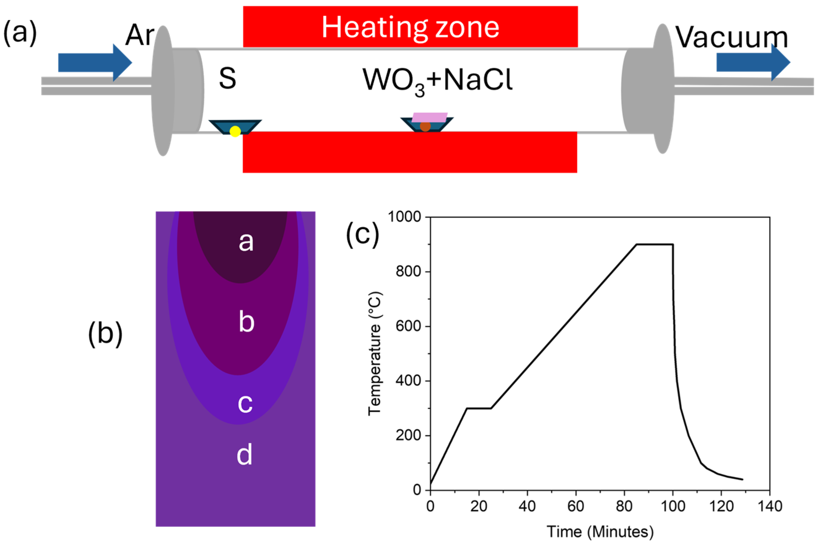
WS2 crystals were grown on SiO2/Si substrates with a 300 nm thick thermal oxide layer by LP-CVD in a single heating zone furnace. Prior to growth, the nominally 5 cm long, 1.9 cm wide substrates were cleaned through a series of 15 min ultrasonication steps in acetone, isopropanol, and de-ionized water, respectively. Sulfur and tungsten oxide powders were precursor materials, with NaCl as a promotor material. A total of 500 mg of sulfur (99.98% purity, Sigma-Aldrich, St. Louis, MO, USA), and a mixture of 50 mg of WO3 (99.9% purity, Sigma-Aldrich) were placed in two different alumina combustion boats of 10 mm in height and 6 cm in length. Subsequently, 2.5 mg of NaCl (99.5% purity, Sigma-Aldrich) was mixed into the boat containing WO3. The WO3/NaCl mixture was placed near the leading edge of the boat. The boats were loaded in a quartz tube with an inner diameter of 44 mm, with the substrate was placed on top of the combustion boat containing the mixture of WO3 and NaCl, with the leading edge of the substrate aligned with the center of the mixture. A schematic of the LPCVD set-up used for the growth of WS2 films is shown in Figure 1a. The boat was placed in the central heating zone while the sulfur was placed at the edge of the heating zone to control the vapor flow and prevent the early evaporation of sulfur.

Figure 1.
(a) Schematic of the CVD set-up and (b) a diagram depicting a typical zonal growth pattern, with different regions (a–d) corresponding to bulk, large flakes, transitioning to smaller, isolated growth, and no growth regions, respectively. (c) The temperature profile used during heating, growth, and cooling.
After reaching a base pressure of nominally 400 mTorr, the tube was purged with 500 SCCM of argon gas. The tube was then heated to 300 °C in 15 min and allowed to sit at 300 °C under Ar flow for 10 min. The temperature of the furnace was then increased to the growth temperature at the rate of 10 °C per minute. The growth of the sample was carried out at temperatures of 700 °C, 800 °C, and 900 °C for 15 min. During the growth, the temperature of the crucible containing sulfur was fixed at nominally 180 °C. At each temperature, the flow rate of Ar was chosen to be either 25, 50, or 75 SCCM, allowing for the role of both temperature and flow rate on the resultant morphology to be observed. Following growth, the sample was rapidly cooled down to room temperature. The temperature profile for growth at 900 °C is shown in Figure 1c and is similar for all temperatures studied. The process pressure for growth at 25, 50, and 75 SCCM was approximately 1.2, 1.5, and 1.8 Torr, respectively.
Following growth, the sample’s chemical composition was examined by X-ray photoemission spectroscopy (XPS) using a Thermo Scientific (Waltham, MA, USA) K-Alpha XPS system with a 0.1 eV step size. The presence of WS2 was also confirmed by Raman spectroscopy in a standard backscattering geometry and a 50x objective at room temperature using a Thermo Scientific DXR Raman Microscope with a 532 nm laser. An 1800 line/mm grating and a 50 μm slit aperture were used. Measurements were carried out near the region’s center at various distances from the upstream edge of the substrate. Raman data were smoothed using a Savitzky–Golay filter. The variation in the morphology was studied using a Hitachi-4700 (Tokyo, Japan) field emission scanning electron microscope (FESEM) at an accelerating voltage of 10 kV and an emission current of 10 µA.
3. Results
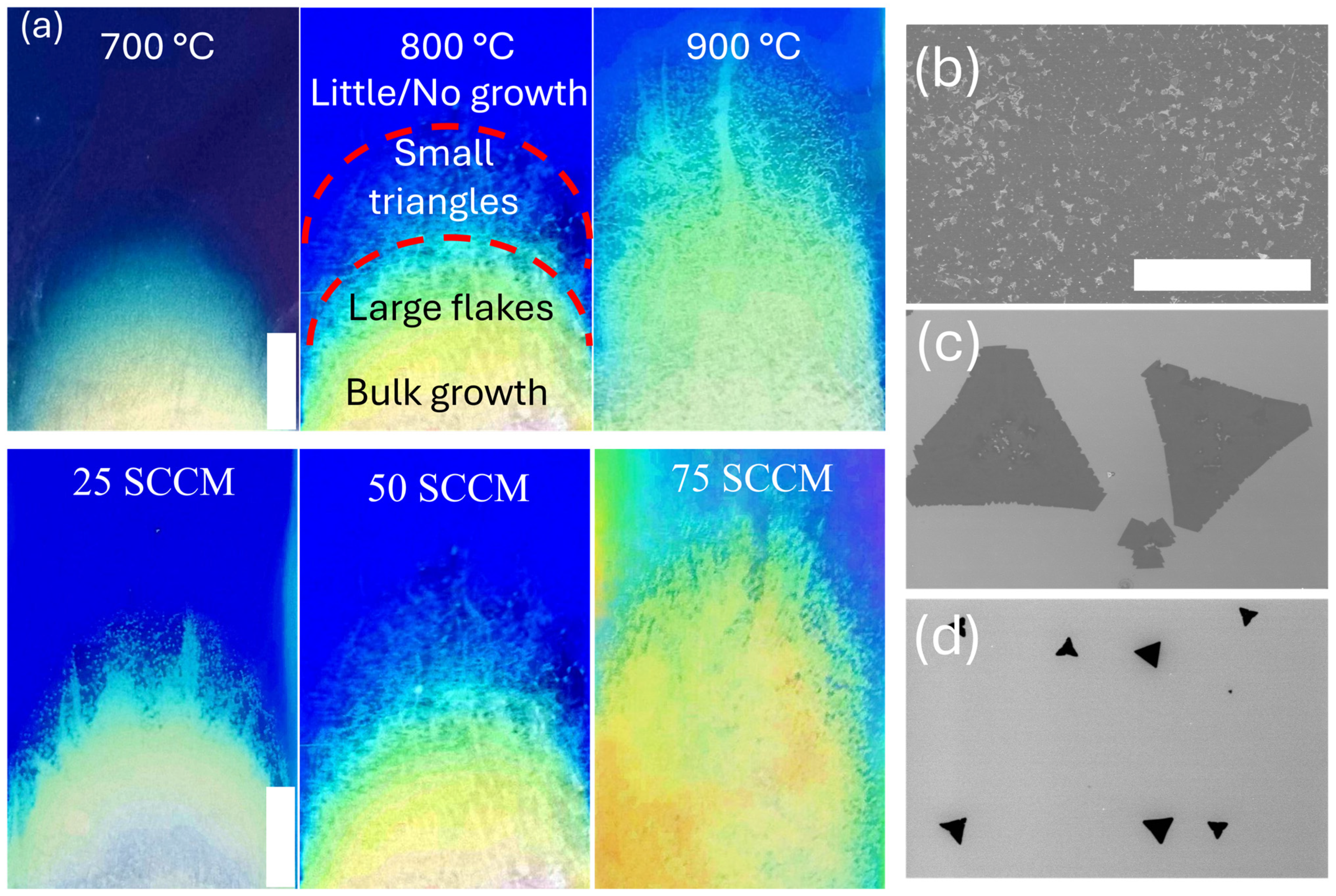
Figure 2 shows the typical zonal growth pattern [30,31] for samples grown under varying temperatures and flow rates. Increasing the temperature or the flow rate leads to a more extensive growth region, as expected. Along the leading edge of the substrate, which is close to the WO3 precursor, we observe mostly bulk growth, with growth transitioning to thin, isolated crystals, with size and density decreasing further from the leading edge. The extent of the growth and width of each region grows with both increasing temperature and flow rate, which is expected due to the increased precursor quantity and reaction rates resulting from both.

Figure 2.
(a) Optical images showing the zonal growth pattern and relative extent of growth for (top) varying temperatures at a flow rate of 50 SCCM and (bottom) at varying flow rates at 800 °C, and representative SEM images in the region of (b) 0–1 cm, (c) 1–2 cm, and (d) 2–3 cm along the midpoint of the growth zone. The scale bar is 1 cm for (a) and 100 µm for (b–d).
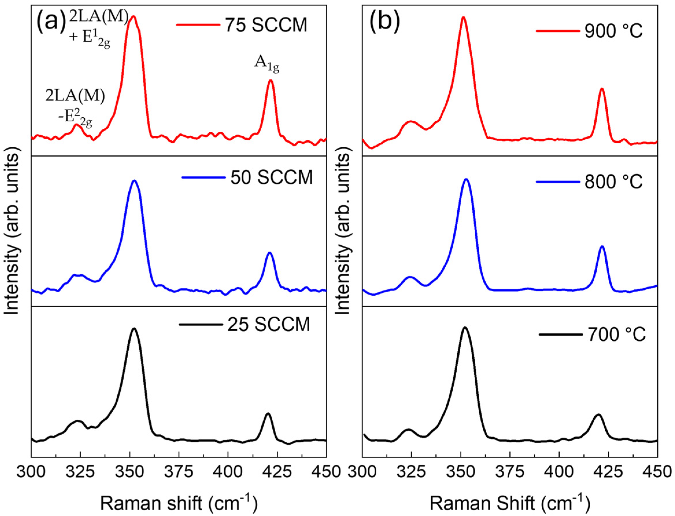
Raman spectroscopy, shown in Figure 3, confirmed that this growth corresponds to WS2. Raman measurements were taken in the central region 2 cm downstream from the leading edge of the substrate, as shown in Figure 4. Three primary peaks were observed for all samples at nominally 323, 352, and 420 cm−1, in good agreement with that of mechanically exfoliated WS2 and suggesting a lack of significant doping of halide or alkali metal atoms [26]. The peak at 352 cm−1 is a convolution of the in-plane vibrational E12g mode and a second-order mode of the longitudinal acoustic phonon 2LA(M) peak. The peak near 420 cm−1 corresponds to the out-of-plane vibrational A1g mode, while the peak around 323 cm−1 has been previously reported to result from a 2LA(M)-E22g hybrid mode [32,33]. As the peak separation between E12g and A1g increases with increasing layer number, the difference between these peaks from sample to sample may be used to identify increased growth thickness [34]. At a fixed temperature of 800 °C, the peak separation changes from 67.2 cm−1 at 25 SCCM to 68.2 cm−1 at 50 SCCM and 68.9 cm−1 at 75 SCCM, indicating that increased flow rates resulted in thicker growth at equal distances downstream, which is consistent with the greater growth observed in optical images shown in Figure 2a. Further, increasing flow rates results in an increasing A1g/E12g intensity ratio, which is also associated with increasing growth at a given downstream distance. Similarly, peak separations of 66.3, 68.3, and 69.6 cm−1 were found for growth at a constant 50 SCCM flow rate and temperatures of 700, 800, and 900 °C, respectively, consistent with expected increasing thicknesses at a fixed position for increasing temperatures. For all samples, Raman spectra indicate growths of between 1 and 4 layers [11].
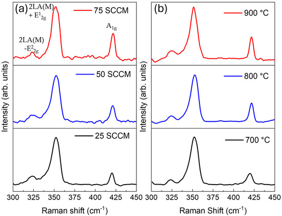
Figure 3.
Raman spectra for samples grown at (a) 800 °C and varying flow rates, and (b) varying temperatures and a fixed 50 SCCM flow rate. Measurements were taken 2 cm from the leading edge of the substrate. Note that measurements taken at 50 SCCM were taken from different samples. However, this does not result in changes to the Raman spectra. Raman modes are marked in (a).

Figure 4.
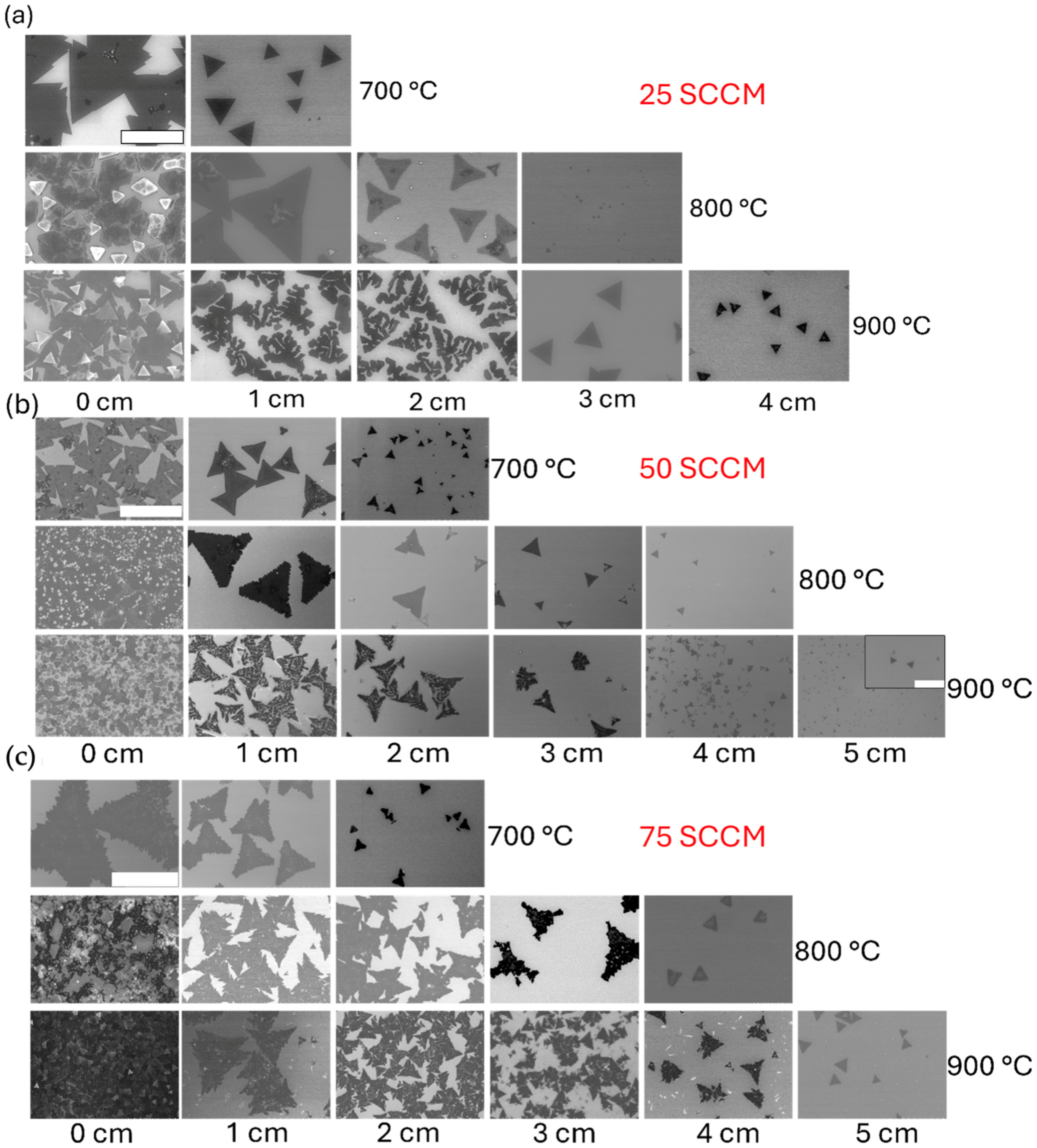
SEM images at various distances along the leading edge of the substrate for varying temperatures at a constant flow rate of (a) 25 SCCM, (b) 50 SCCM, and (c) 75 SCCM. The scale bar is 10 µm for all images in (a) and 100 µm in (b) and (c). The magnified image on the inset (b) has a scale bar of 10 µm and indicates small-scale triangular growth.
SEM images at 25 SCCM are shown in Figure 4a, with representative images taken at given substrate locations for varying flow rates to understand changes in morphology driven by flow rate and temperature. The total growth region increases as the temperature increases, with more growth downstream. At 700 °C, thin triangular crystals are observed both at the substrate leading edge and 1 cm downstream. Increasing temperatures lead to growth up to 4 cm and also drastic morphology changes, which are especially apparent at 900 °C, wherein the triangular structure becomes disordered, with similar structures referred to as dendritic, fractal, or semi-compact growth in previous works [24,25,27,35,36]. However, increasing the downstream distance decreases the overall structure size while the ordered triangular crystal structure is recovered. This recovery of triangular growth occurs at greater distances for increased temperatures or flow rates. At 50 SCCM, a similar transition is apparent, as shown in Figure 4b. However, the disordered transition occurs at the lower temperature of 800 °C, with a significantly larger disorder apparent at 900 °C and disordered growth extending further downstream. At 75 SCCM, as shown in Figure 4c, disordered growth appears even at 700 °C, and the disordered region at higher temperatures extends to even more distant regions of the substrate. It is apparent that both increased flow rate and temperature significantly enhance this transition to disordered growth. However, all structures retain a semi-compact triangular form. Even at the lowest temperatures, increasing flow rates result in disordered edges. For all samples, increasing the distance from the source results in lower density growth and the decreased size of individual elements, as expected owing to the gradient in metal precursor availability further from the substrate leading edge.
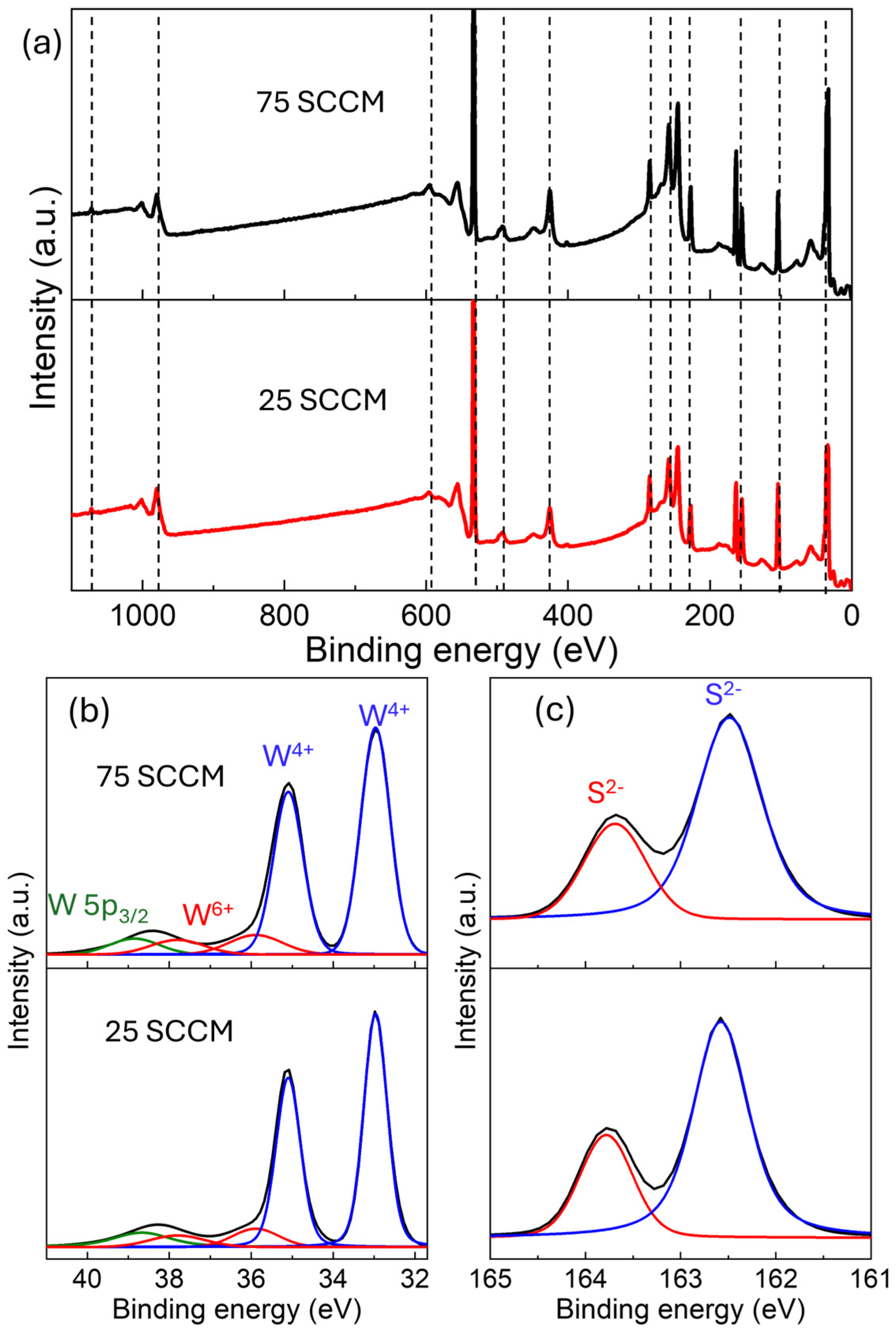
XPS measurements, shown in Figure 5, were taken 1 cm downstream from samples grown at 800 °C and 25 and 75 SCCM flow rates. Survey spectra indicate only small amounts of NaCl are present following growth, as indicated by the barely noticeable Na 1s peak. W 4f and S 2p signals are shown in Figure 5b,c, with fitting to Voigt profiles for each peak performed using the method described in [37]. The W 4f signal is comprised of W 4f5/2 and W 4f7/2 doublets belonging to W6+ and W4+ oxidation states, as well as a contribution from the W 5p3/2 state at a slightly higher binding energy. Fits assumed an area ratio between corresponding doublets of 4:3 per the multiplicity of corresponding levels, as well as equal line widths. The W4+ peaks are centered at binding energies of 35.1 and 33.0 eV for W 4f5/2 and W 4f7/2, respectively, which are characteristic of WS2, with no noticeable shift for both samples. Additional peaks corresponding to W6+, characteristic of WO3, are found at 37.8 and 35.9 eV. Binding energies for the S 2p doublet corresponding to S 2p1/2 and S 2p3/2 states are found at 163.8 and 162.5 eV for both samples. As no significant differences in intensity ratios or peak locations for W4+ and W6+ species are observed between samples, the transformation is not associated with changes to the local chemical environment and instead is related to the kinetics of crystal growth of similar species at the surface.
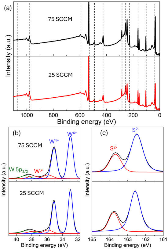
Figure 5.
XPS spectra correspond with samples grown at 800 °C and the indicated flow rates. (a) Survey spectra showing the Na 1s, O KLL, W 4s, O 1s, W 4P1/2, W 4p3/2, C 1s, W 4d, S 2s, S 2p, Si 2p, and W 4f states in the order of decreasing binding energy. (b,c) show high-resolution scans corresponding to the W 4f and S2p states. The different rows in (b) and (c) represent flow rates indicated in (b).
4. Discussion
The transition from regular triangular to dendritic growth is explained by the competition between attachment rates to the nucleated structures, detachment, and edge diffusion rates. Adatoms can diffuse along the edge for slow growth to form the most stable configuration, resulting in compact domains. However, if the attachment rate is too high or the diffusion rate too low, adatoms can no longer sufficiently diffuse to the lowest energy sites [25,35,38,39]. Kinetic Monte Carlo (KMC) studies have shown that the degree of edge disorder and transition to dendritic growth at a given temperature is then related to the total flux and flux ratio of chalcogen and transition metals (C/M ratio) [36]. For example, at a low metal flux, growth was shown to produce compact triangles with no sensitivity to the C/M ratio. However, increasing the metal flux while maintaining a low C/M ratio leads to the growth of semi-compact, disordered triangular structures similar to those observed in our works. It is clear that increasing temperature at the growth site and the WO3/NaCl mixture will result in an increased metal flux while maintaining the same flux of S to the substrate and, therefore, can drive the transition from triangular to semi-compact structures seen in this work, as this will result in maintaining a low C/M ratio while enhancing the metal flux. Similarly, the recovery of triangular growth further downstream may be explained by decreasing tungsten precursor concentrations with distance from the source material. The role of flow rate is somewhat more complex. Increasing flow rates can enhance the mass transfer process, transforming growth from thermodynamic to kinetic [20]. While both chalcogen and metal flux increase in this scenario, the ratio may not significantly change. As a result, flux may play a similar role to temperature in determining the morphology through primarily modulating the metal flux while having a lesser effect on the C/M ratio. This is further supported by the observation of a transition from straight to curved-edge triangular growth, as shown in Figure 6, wherein this describes how well the edge conforms to a straight line connecting triangle vertices. For all semi-compact domains, a curve away from a straight line is clearly visible, which reverses midway through the given edge. This structure has been reported previously to result from an imbalance of the C/M ratio and can be driven by either too high measures of chalcogen or metal fluxes [20]. The recovery of the straight edge with increasing distance downstream indicates that this is the result of a C/M ratio that is too low, wherein the ratio increases further downstream. Similar deviations from straight-line edges were also demonstrated for semi-compact growth in KMC models [36].
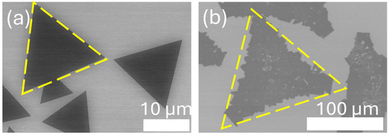
Figure 6.
SEM images show the emergence of deviations from straight-edge triangular growth as the flow rate is increased from (a) 25 SCCM to (b) 75 SCCM. Otherwise, images are taken under identical growth conditions at 700 °C and 1 cm downstream.
5. Conclusions
We have grown WS2 crystals with low-pressure CVD on thermally oxidized Si substrates. We observe a transition from small, smooth triangles to large, semi-compact growth with zagged edges by systematically varying the temperature and carrier gas flow rate. The physical and chemical properties of synthesized samples have been analyzed with the help of optical microscopy, Raman spectroscopy, X-ray photoelectron spectroscopy (XPS), and SEM. In line with previous reports, increasing metal flux and decreasing the C/M ratio transforms a sample from traditional compact triangular growth to more complex, semi-compact growth with significant disorder while maintaining a roughly triangular structure. Temperature enhances metal flux via the increased evaporation and decomposition of the WO3 precursor itself. Meanwhile, flow rate modifications play a similar, albeit more complicated, role by enhancing both metal and sulfur flux. However, our results indicate that metal flux enhancements play a dominant role, resulting in changes in morphology similar to those caused by enhancing temperature. The ability to control the morphology of the 2D-TMDC by controlling the process parameters has important applications in optoelectronics and electrochemistry, allowing for the enhancement or suppression of disorder while also allowing for the tunability of the number of active edge sites.
Author Contributions
Conceptualization, H.P. and S.P.; methodology, H.P. and S.P.; formal analysis, H.P., S.P. and S.M.; investigation, H.P.; resources, S.P and S.M.; data curation, H.P.; writing—original draft preparation, S.P. and H.P.; writing—review and editing, H.P., S.P. and S.M.; visualization, H.P. and S.P.; supervision, S.P.; project administration, S.P. All authors have read and agreed to the published version of the manuscript.
Funding
This research received no external funding.
Data Availability Statement
Data supporting the conclusions of this article will be made available by the authors on request.
Acknowledgments
Support for XPS measurements from Felio Perez at the University of Memphis Integrated Microscopy Center for XPS measurement is greatly appreciated.
Conflicts of Interest
The authors declare no conflicts of interest.
References
- Ovchinnikov, D.; Allain, A.; Huang, Y.-S.; Dumcenco, D.; Kis, A. Electrical Transport Properties of Single-Layer WS2. ACS Nano 2014, 8, 8174–8181. [Google Scholar] [CrossRef]
- Shi, S.; Liang, S.; Zhu, Z.; Cai, K.; Pollard, S.D.; Wang, Y.; Wang, J.; Wang, Q.; He, P.; Yu, J.; et al. All-electric magnetization switching and Dzyaloshinskii-Moriya interaction in WTe2/ferromagnet heterostructures. Nat. Nanotechnol. 2019, 14, 945–949. [Google Scholar] [CrossRef]
- Xiao, D.; Liu, G.-B.; Feng, W.; Xu, X.; Yao, W. Coupled Spin and Valley Physics in Monolayers of MoS 2 and and Other Group-VI Dichalcogenides. Phys. Rev. Lett. 2012, 108, 196802. [Google Scholar] [CrossRef]
- Zhu, Z.Y.; Cheng, Y.C.; Schwingenschlögl, U. Giant spin-orbit-induced spin splitting in two-dimensional transition-metal dichalcogenide semiconductors. Phys. Rev. B 2011, 84, 153402. [Google Scholar] [CrossRef]
- Wurstbauer, U.; Miller, B.; Parzinger, E.; Holleitner, A.W. Light–matter interaction in transition metal dichalcogenides and their heterostructures. J. Phys. D Appl. Phys. 2017, 50, 173001. [Google Scholar] [CrossRef]
- Cao, J.; Fiore, S.; Klinkert, C.; Vetsch, N.; Luisier, M. Light-matter interactions in van der Waals photodiodes from first principles. Phys. Rev. B 2022, 106, 035306. [Google Scholar] [CrossRef]
- Wang, Q.H.; Kalantar-Zadeh, K.; Kis, A.; Coleman, J.N.; Strano, M.S. Electronics and optoelectronics of two-dimensional transition metal dichalcogenides. Nat. Nanotechnol. 2012, 7, 699–712. [Google Scholar] [CrossRef]
- Zhao, W.; Ghorannevis, Z.; Chu, L.; Toh, M.; Kloc, C.; Tan, P.-H.; Eda, G. Evolution of Electronic Structure in Atomically Thin Sheets of WS2 and WSe2. ACS Nano 2013, 7, 791–797. [Google Scholar] [CrossRef]
- Braga, D.; Lezama, I.G.; Berger, H.; Morpurgo, A.F. Quantitative Determination of the Band Gap of WS2 with Ambipolar Ionic Liquid-Gated Transistors. Nano Lett. 2012, 12, 5218–5223. [Google Scholar] [CrossRef]
- Voiry, D.; Mohite, A.; Chhowalla, M. Phase engineering of transition metal dichalcogenides. Chem. Soc. Rev. 2015, 44, 2702–2712. [Google Scholar] [CrossRef]
- Zeng, H.; Liu, G.-B.; Dai, J.; Yan, Y.; Zhu, B.; He, R.; Xie, L.; Xu, S.; Chen, X.; Yao, W.; et al. Optical signature of symmetry variations and spin-valley coupling in atomically thin tungsten dichalcogenides. Sci. Rep. 2013, 3, 1608. [Google Scholar] [CrossRef]
- Nayak, P.K.; Lin, F.-C.; Yeh, C.-H.; Huang, J.-S.; Chiu, P.-W. Robust room temperature valley polarization in monolayer and bilayer WS2. Nanoscale 2016, 8, 6035–6042. [Google Scholar] [CrossRef]
- Hwang, W.S.; Remskar, M.; Yan, R.; Protasenko, V.; Tahy, K.; Chae, S.D.; Zhao, P.; Konar, A.; Xing, H.; Seabaugh, A.; et al. Transistors with chemically synthesized layered semiconductor WS2 exhibiting 105 room temperature modulation and ambipolar behavior. Appl. Phys. Lett. 2012, 101, 013107. [Google Scholar] [CrossRef]
- Iqbal, M.W.; Iqbal, M.Z.; Khan, M.F.; Shehzad, M.A.; Seo, Y.; Park, J.H.; Hwang, C.; Eom, J. High-mobility and air-stable single-layer WS2 field-effect transistors sandwiched between chemical vapor deposition-grown hexagonal BN films. Sci. Rep. 2015, 5, 10699. [Google Scholar] [CrossRef]
- Bin Rafiq, K.S.; Amin, N.; Alharbi, H.F.; Luqman, M.; Ayob, A.; Alharthi, Y.S.; Alharthi, N.H.; Bais, B.; Akhtaruzzaman, M. WS2: A New Window Layer Material for Solar Cell Application. Sci. Rep. 2020, 10, 771. [Google Scholar] [CrossRef]
- Schranghamer, T.F.; Sharma, M.; Singh, R.; Das, S. Review and comparison of layer transfer methods for two-dimensional materials for emerging applications. Chem. Soc. Rev. 2021, 50, 11032–11054. [Google Scholar] [CrossRef]
- Kang, T.; Tang, T.W.; Pan, B.; Liu, H.; Zhang, K.; Luo, Z. Strategies for Controlled Growth of Transition Metal Dichalcogenides by Chemical Vapor Deposition for Integrated Electronics. ACS Mater. Au 2022, 2, 665–685. [Google Scholar] [CrossRef]
- Hussain, S.; Xu, R.; Xu, K.; Lei, L.; Meng, L.; Zheng, Z.; Xing, S.; Guo, J.; Dong, H.; Liaqat, A.; et al. Strain-induced hierarchical ripples in MoS2 layers investigated by atomic force microscopy. Appl. Phys. Lett. 2020, 117, 153102. [Google Scholar] [CrossRef]
- Chen, F.; Su, W.; Zhao, S.; Lv, Y.; Ding, S.; Fu, L. Morphological evolution of atomically thin MoS2 flakes synthesized by a chemical vapor deposition strategy. CrystEngComm 2020, 22, 4174–4179. [Google Scholar] [CrossRef]
- Wang, S.; Rong, Y.; Fan, Y.; Pacios, M.; Bhaskaran, H.; He, K.; Warner, J.H. Shape Evolution of Monolayer MoS2 Crystals Grown by Chemical Vapor Deposition. Chem. Mater. 2014, 26, 6371–6379. [Google Scholar] [CrossRef]
- Saenz, G.A.L.; Biswas, C.; Yamaguchi, H.; Villarrubia, C.N.; Mohite, A.D.; Kaul, A.B. Effects of Synthesis Parameters on CVD Molybdenum Disulfide Growth. MRS Adv. 2016, 1, 2291–2296. [Google Scholar] [CrossRef]
- Pokhrel, H.; Duncan, J.J.A.; Woli, Y.B.; Hoang, T.B.; Pollard, S.D. The effect of Ar plasma on the space-confined growth of MoS2 with low-pressure chemical vapor deposition. AIP Adv. 2023, 13, 065322. [Google Scholar] [CrossRef]
- Wu, L.; Yang, W.; Wang, G. Mechanism of substrate-induced anisotropic growth of monolayer WS2 by kinetic Monte Carlo simulations. NPJ 2D Mater. Appl. 2019, 3, 6. [Google Scholar] [CrossRef]
- Xu, W.; Li, S.; Zhou, S.; Lee, J.K.; Wang, S.; Sarwat, S.G.; Wang, X.; Bhaskaran, H.; Pasta, M.; Warner, J.H. Large Dendritic Monolayer MoS2 Grown by Atmospheric Pressure Chemical Vapor Deposition for Electrocatalysis. ACS Appl. Mater. Interfaces 2018, 10, 4630–4639. [Google Scholar] [CrossRef]
- Ma, J.; Li, X.; Gan, L.; Zhang, S.; Cao, Y.; Nie, Z.; Wang, X.; Ma, D.; He, L.; Nie, J.; et al. Controlling the dendritic structure and the photo-electrocatalytic properties of highly crystalline MoS2 on sapphire substrate. 2D Mater. 2018, 5, 031015. [Google Scholar] [CrossRef]
- Li, S.; Wang, S.; Tang, D.-M.; Zhao, W.; Xu, H.; Chu, L.; Bando, Y.; Golberg, D.; Eda, G. Halide-assisted atmospheric pressure growth of large WSe2 and WS2 monolayer crystals. Appl. Mater. Today 2015, 1, 60–66. [Google Scholar] [CrossRef]
- Pokhrel, H.; Duncan, J.J.A.; Krause, B.; Hoang, T.B.; Pollard, S.D. Transformation from dendritic to triangular growth of WS2 via NaCl assisted low-pressure chemical vapor deposition. J. Vac. Sci. Technol. A 2024, 42, 042203. [Google Scholar] [CrossRef]
- Di, X.; Wang, F.; Wei, J.; Shen, J.; Zhang, B.; Shan, X.; Lin, X.; Hao, Y.; Zhang, K. Controlled synthesis of WS2 with different layers by tuning flow rates. Mater. Sci. Eng. B 2020, 261, 114756. [Google Scholar] [CrossRef]
- Lin, X.; Liu, Y.; Wang, K.; Wei, C.; Zhang, W.; Yan, Y.; Li, Y.J.; Yao, J.; Zhao, Y.S. Two-Dimensional Pyramid-like WS2 Layered Structures for Highly Efficient Edge Second-Harmonic Generation. ACS Nano 2018, 12, 689–696. [Google Scholar] [CrossRef]
- Somphonsane, R.; Chiawchan, T.; Bootsa-Ard, W.; Ramamoorthy, H. CVD Synthesis of MoS2 Using a Direct MoO2 Precursor: A Study on the Effects of Growth Temperature on Precursor Diffusion and Morphology Evolutions. Materials 2023, 16, 4817. [Google Scholar] [CrossRef]
- Chiawchan, T.; Ramamoorthy, H.; Buapan, K.; Somphonsane, R. CVD Synthesis of Intermediate State-Free, Large-Area and Continuous MoS2 via Single-Step Vapor-Phase Sulfurization of MoO2 Precursor. Nanomaterials 2021, 11, 2642. [Google Scholar] [CrossRef]
- Chen, Y. Growth of a Large, Single-Crystalline WS2 Monolayer for High-Performance Photodetectors by Chemical Vapor Deposition. Micromachines 2021, 12, 137. [Google Scholar] [CrossRef]
- Lee, Y.-H.; Yu, L.; Wang, H.; Fang, W.; Ling, X.; Shi, Y.; Lin, C.-T.; Huang, J.-K.; Chang, M.-T.; Chang, C.-S.; et al. Synthesis and Transfer of Single-Layer Transition Metal Disulfides on Diverse Surfaces. Nano Lett. 2013, 13, 1852–1857. [Google Scholar] [CrossRef]
- Berkdemir, A.; Gutiérrez, H.R.; Botello-Méndez, A.R.; Perea-López, N.; Elías, A.L.; Chia, C.-I.; Wang, B.; Crespi, V.H.; López-Urías, F.; Charlier, J.-C.; et al. Identification of individual and few layers of WS2 using Raman Spectroscopy. Sci. Rep. 2013, 3, 1755. [Google Scholar] [CrossRef]
- Chowdhury, S.; Roy, A.; Bodemann, I.; Banerjee, S.K. Two-Dimensional to Three-Dimensional Growth of Transition Metal Diselenides by Chemical Vapor Deposition: Interplay between Fractal, Dendritic, and Compact Morphologies. ACS Appl. Mater. Interfaces 2020, 12, 15885–15892. [Google Scholar] [CrossRef]
- Nie, Y.; Liang, C.; Zhang, K.; Zhao, R.; Eichfeld, S.M.; Cha, P.-R.; Colombo, L.; A Robinson, J.; Wallace, R.M.; Cho, K. First principles kinetic Monte Carlo study on the growth patterns of WSe2 monolayer. 2D Mater. 2016, 3, 025029. [Google Scholar] [CrossRef]
- Chen, P.; Baldwin, M.; Bandaru, P.R. Hierarchically structured, oxygen deficient, tungsten oxide morphologies for enhanced photoelectrochemical charge transfer and stability. J. Mater. Chem. A 2017, 5, 14898–14905. [Google Scholar] [CrossRef]
- Chen, S.; Gao, J.; Srinivasan, B.M.; Zhang, G.; Sorkin, V.; Hariharaputran, R.; Zhang, Y.-W. Origin of ultrafast growth of monolayer WSe2 via chemical vapor deposition. npj Comput. Mater. 2019, 5, 28. [Google Scholar] [CrossRef]
- Nie, Y.; Liang, C.; Cha, P.-R.; Colombo, L.; Wallace, R.M.; Cho, K. A kinetic Monte Carlo simulation method of van der Waals epitaxy for atomistic nucleation-growth processes of transition metal dichalcogenides. Sci. Rep. 2017, 7, 2977. [Google Scholar] [CrossRef]
Disclaimer/Publisher’s Note: The statements, opinions and data contained in all publications are solely those of the individual author(s) and contributor(s) and not of MDPI and/or the editor(s). MDPI and/or the editor(s) disclaim responsibility for any injury to people or property resulting from any ideas, methods, instructions or products referred to in the content. |
© 2024 by the authors. Licensee MDPI, Basel, Switzerland. This article is an open access article distributed under the terms and conditions of the Creative Commons Attribution (CC BY) license (https://creativecommons.org/licenses/by/4.0/).

