Article

Design and Experimental Verification of Electric Vehicle Battery Charger Using Kelvin-Connected Discrete MOSFETs and IGBTs for Energy Efficiency Improvement

Warwick Manufacturing Group, Warwick University, Coventry CV4 7AL, UK
*
Author to whom correspondence should be addressed.
Electricity 2024, 5(4), 684-711; https://doi.org/10.3390/electricity5040034
Submission received: 18 July 2024 / Revised: 22 September 2024 / Accepted: 25 September 2024 / Published: 30 September 2024

Abstract

:
This research investigates the advantages of Kelvin-connected 4-pin discrete transistors, both MOSFETs and IGBTs, in onboard battery chargers for electric vehicles. The study compares the standard 3-pin and the extended 4-pin packages based on averaged data collected from leading manufacturers. The investigation shows significant potential power loss reduction, thermal operation mitigation, and reduced gate-drive oscillation for the 4-pin package. The benefits have been quantified by analysing the operation of actual switches in an automotive battery charger based on Boost-PFC and DC-DC LLC converters. The converters’ practical design demonstrates a procedure for integrating the Kelvin-connected package into the design methodology. The results have been verified experimentally.

1. Introduction

Battery chargers for automotive applications are one of the main onboard sub-systems of electric vehicles. Like all other pieces of electronics, high efficiency, power density, reliability, and ease of thermal management are vital. To fulfil these needs, this study investigates 4-pin Kelvin-connected discrete MOSFETs and IGBTs, which offer advanced characteristics potentially leading to power loss and temperature reductions.
The advantages of Kelvin-connected MOSFETs have been well evaluated with analytical models based on equivalent circuits, supported by experimental verification [1,2,3,4,5]. In [1], the research focuses on the influence of gate-drive resistance on the drain current spike and oscillations during turn-on and turn-off. The importance of minimising parasitic inductance in the gate-drive circuit, which takes advantage of the Kelvin-connected 4-pin package’s full potential, is analysed in [2]. This paper also analyses the effects of external factors, such as PCB layouts and gate-drive elements. The model in [3] includes device and circuit layout parasitics, exploring the effective transconductance during transients. The targeted maximum parasitic common source inductance criterion is 3   n H , as given in [4]. Assuming the above requirements for the package have been implemented, the Kelvin connection can also improve the reverse-recovery phenomenon associated with the body diode, as shown in [5].
Many studies have demonstrated the advantages of the Kelvin-connected 4-pin package by directly comparing it to the standard 3-pin through-hole package [6,7,8,9]. A reliability comparison between the two packages was conducted in [6] with High Electric Field (HEF) and Active Channel Gate Bias (ACGB) tests. The experimental results show that, generally, 3-pin packages are more tolerant to short circuits due to their higher source inductance and resistance. The research demonstrates a disadvantage of Kelvin-connected packages, which must be mitigated by providing over-current protection to ensure the same level of reliability. In a similar case, in [7,8], both packages’ dynamic parameters were compared, and the blanking time of the desaturation protection scheme for the power modules was studied. The parasitic inductances for the standard 3-pin package are in the range of 5 10   n H , while those for the Kelvin package are estimated to be 0.2 1   n H [8]. The comparison in [9] shows the Kelvin-connected 4-pin advantage over the exact 3-pin counterpart applied in a Boost-PFC converter. The same research also specified the optimal gate-drive resistors for the Kelvin-connected package as 18 Ω, being a trade-off between the oscillations at the gate-drive circuit, EMI, and the transistors’ dynamic performance in that particular case.
The ability to use transistors in parallel is used to increase the current-handling capability. Research in this direction shows that by meeting specific requirements, Kelvin-connected devices could offer some advantages when connected in parallel [10,11,12,13,14]. A passive balancing method applied to Kelvin-connected SiC MOSFETs using a differential mode choke without additional active control was proposed in [10]. The undesirable effect of crosstalk was investigated further in [11], applying techniques for Gate Impedance Regulation (GIR) and Gate Voltage Regulation (GVR). The impact of an asymmetric layout on current balancing was analysed in [12]. It has been shown that current balancing strongly depends on the quality of the gate-drive circuit, particularly the prevention of gate-drive oscillations [13]. For this reason, in [14], additional resistors in the Kelvin circuit were utilised between the emitter and the gate driver, which was demonstrated with 4-pin IGBTs. The study recommends resistors in the range of 0.5 1   connected in series to the driver.
Additional benefits of the Kelvin connection in both MOSFETs and IGBTs have been objects of research in several studies [15,16,17,18,19,20,21]. In [15], online bond wire fault monitoring was proposed, and with a similar topology [16], it offers short-circuit, overload, and gate-drive protection for high-voltage MOSFET modules. Because such overloads apply significant stress, a comprehensive study on consequent thermal–electrical degradation was undertaken in [17]. Finally, the main benefit of the Kelvin connection—improved dynamic characteristics leading to loss reduction—was shown in [18,19]. These advantages make the Kelvin-connected transistors the right choice for critical automotive applications, as proven in [20,21].
Similar studies have been dedicated to discrete Kelvin-connected IGBTs and SiC MOSFETs. According to the comparison conducted in [22,23,24] and the 4-pin package analysis [25], the switching loss for Kelvin-connected SiC MOSFET is 60 % [23] to 80 % [22] reduced compared to Si IGBTs, reducing the junction temperature by 38 % [23]. Also, a comparison between the 3-pin and 4-pin IGBTs demonstrated an improved power density with the TO-247PLUS package due to the reduced number of paralleled transistors [24]. The expected switching power loss reduction by using IGBTs in a 4-pin package is up to 10 % compared to the identical transistors in a 3-pin TO-247 package [25]. Further power density and efficiency improvements were reported due to IGBTs with TRENCHSTOP technology [26], giving up to 15 % more output current, and these IGBTs are also offered in the TO-247PLUS package. The measurement techniques and protection abilities of Kelvin-connected IGBTs were reported in [27,28,29,30] for discrete packages and modules.
Power density and efficiency are the central requirements for automotive applications, including onboard battery chargers. One of the topologies offering high efficiency is the LLC DC-DC converter, widely used in battery chargers [31,32,33,34,35,36,37,38,39,40,41]. The reported efficiency in [31] is 94.6 % at 2.7   k W , operating with a combination of Pulse Frequency Modulation (PFM) and Pulse Width Modulation (PWM) for light-load operation. The topology is applicable for low-voltage (LV) [31,34,35,36,39,41] and high-voltage (HV) [32,37,38] battery chargers. A similar efficiency of 94.3 % was reported in [32] for a train application charger rated at 25   k W . The switching frequency using SiC MOSFETs can reach 1   M H z , achieving 95.8 % efficiency over the battery voltage range, as experimentally shown for an 11   k W charger in [33]. In [35], a frequency range between 91   k H z and 110   k H z was applied, giving 96.9 % efficiency with a five-level LLC converter. Similar multi-level techniques have been demonstrated with a series–parallel connection of two transformers [37], reducing the size and the core power loss and improving heat dissipation. The same benefits are achievable with an interleaved LLC topology, as shown in [38], giving 95.65% peak efficiency for a converter with 1.5 kW maximum power. A three-phase topology was described in [39]. Optimal transformer design techniques were presented in [40], and the low-voltage output ( 28   V ) with a relatively high output current ( 50   A ) solution was suggested in [41].
The Power Factor Correction (PFC) converter is mandatory for offline chargers [42,43,44,45,46,47,48,49,50,51,52,53,54,55,56,57]. The DC-DC topologies used are Boost, semi-bridgeless, and bridgeless. The review in [42] presents their advantages and disadvantages. Many studies report the superior efficiency of bridgeless converters [43,44,45,46,47] based on the Totem-pole topology with GaN HEMTs. However, the circuit is distinguished by increased complexity and price due to the expensive GAN transistors. Therefore, the DC-DC Boost-PFC converter is still preferred for many applications, offering a good quality/price ratio [48,49,50,51,52,53,54,55,56,57].
Although PFC-Boost is a well-known topology, its development and improvement are still in progress. A modification of the PFC-Boost feedback circuit to reduce the compensation capacitor, potentially leading to improved reliability and reduced cost, was suggested in [48]. Further, an overall power factor increase can be achieved by applying variable inductances, for example, ranging from 0.193 mH to 0.951 mH [49]. The potential of the Boost-PFC converter to operate with low Electromagnetic Interference (EMI) was shown in [50], and the reduction in the Total Harmonic Distortion (THD) in the supply current to within industrial standards was shown in [51].
The interleaved Buck–Boost and PFC-Boost topologies [52,53,54,55,56,57,58,59] offer additional benefits, like reduced current and, thermal stress on the power switches, more uniform power loss distribution, and improved reliability. To deploy the full potential of the interleaved circuit, some essential issues must be resolved: equalising current sharing [52]; applying soft commutation [53]; increasing the output voltage range with Buck–Boost operation [54,55]; and improving the light-load operation with a coupled inductor [56]. Nevertheless, an interleaved Boost-PFC converter remains a good choice for an onboard battery charger, as demonstrated in [57]. The general utilisation of Buck–Boost converters is a part of the charging system of the electric drivetrain, as shown in [58,59]
The literature review leads to the following conclusions:
  • The advantages of the 4-pin discrete Kelvin-connected MOSFETs [1,2,3,4,5,6,7,8,9,10,11,12,13,14,15,16,17,18,19,20] and IGBT [21,22,23,24,25,26,27,28,29,30] are well demonstrated with models and simulations and supported with experiments. The switches were studied individually and are not associated with a specific converter topology. Therefore, their potential contribution to power loss and temperature reduction in a particular topology requires additional study.
  • Most battery charger converters are based on a PFC-Boost circuit [42,43,44,45,46,47,48,49,50,51,52,53,54,55,56,57], offering a good quality/price ratio and a subsequent LLC [31,32,33,34,35,36,37,38,39,40,41] stage, which is highly efficient due to the ZVS operation. Published results suggest that further improvement could be achieved with Kelvin-connected transistors, but this requires further analytical and experimental investigation. However, no complete study has demonstrated the application of Kelvin-connected discrete IGBTs and MOSFETs in automotive battery chargers.
Based on these conclusions, this research aims to fill the knowledge gap by showing approaches for integrating Kelvin-connected transistors into the Boost-PFC and LLC DC-DC stages in an automotive battery charger, supported by a comparison between the standard 3-pin and Kelvin-connected 4-pin packages. The results quantify the potential benefits by numerically estimating the power loss reduction, temperature decrease, and efficiency improvement. In this sense, the novelty is finding alternative approaches to improving converters based on 4-pin Kelvin-connected TO 247 package transistors, enhancing the battery charger.
The rest of this paper is structured as follows: Section 2 introduces the proposed battery charger architecture and develops the primary mathematical approach to describe the main difference between the two packages; in Section 3 and Section 4, the design of the LLC and PFC-Boost converters are presented, respectively; Section 5 introduces the experimental verification, and the final conclusions are given in Section 6.

2. The Architecture of the Proposed Battery Charger

This part presents the topology of the proposed charger based on discrete Kelvin-connected IGBTs and MOSFETs. Based on 4-lead TO-247PLUS transistors, the potential for power loss reduction, leading to efficiency improvement, is studied analytically, supported by datasheet examples for several off-the-shelf devices.

2.1. The Central Topology of the Proposed Charger

Figure 1 shows the primary circuit of the explored battery charger. This research focuses on two sub-systems: the Boost-PFC DC-DC converter and the LLC DC-DC converter, which operates as a battery charger. As the suggested Kelvin connection benefits apply to the converters’ power parts, control systems and feedback networks are not considered.
The proposed charger comprises the following elements:
  • Single-phase input rectifier (not part of this research).
  • Boost-PFC converter with three channels. Channel 1: Kelvin-connected IGBT Q1, inductor L1, ultra-fast diode D1, and current sense resistor Rcs1. Channel 2: Q2, L2, D2, Rcs2. Channel 3: Q3, L3, D3, and Rcs3. The Boost capacitor C1 is common for all three parallel channels.
  • LLC DC-DC half-bridge converter with Kelvin-connected MOSFETs Q4 and Q5, resonant circuit capacitor C2, transformer with integrated resonant inductor T1, output rectifier ultra-fast diodes D4 and D5, and output filter capacitor C3. The transformer integrates the resonant inductance L r and magnetised inductance L m .

2.2. Investigation of the Application of Kelvin-Connected Discrete MOSFETs and IGBTs in the Suggested Battery Charger

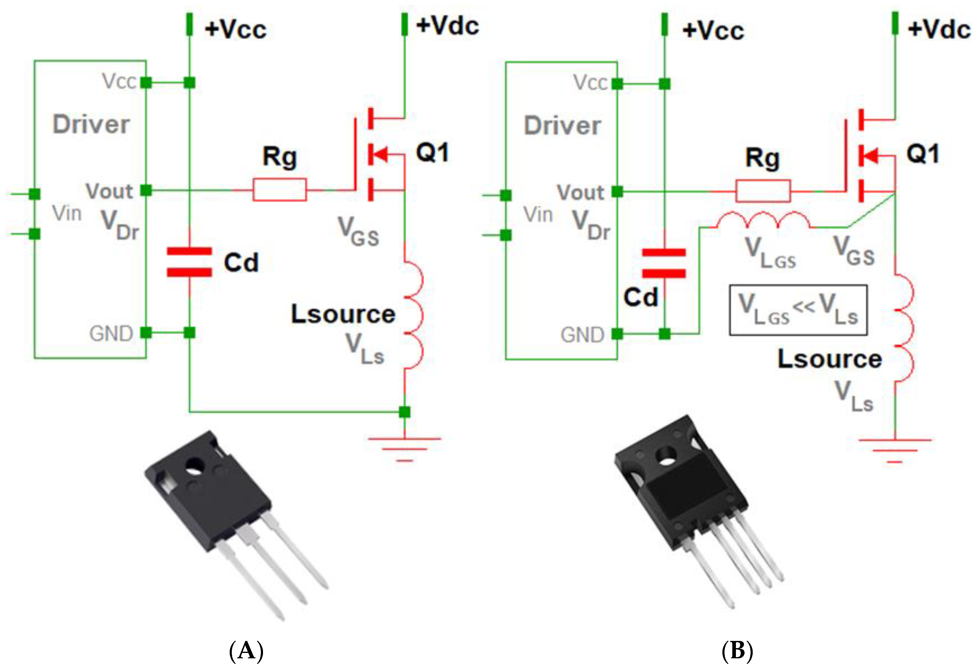
The primary circuits of the standard 3-pin and Kelvin 4-pin TO-247 packages are shown in Figure 2A and Figure 2B, respectively. The main elements are the driver, the gate-drive resistor (Rg), the gate-drive capacitor (Cd), and the parasitic source inductance (Lsource). The same circuit topology and analysis applies to the IGBTs; therefore, they are not presented separately.
As previously explained, the first package includes the parasitic source inductance, L s o u r c e , as a part of the gate-drive loop, the driver V o u t , R g , Q 1 gate-source junction, L s o u r c e , and ground GND. The Kelvin source package isolates L s o u r c e from the gate-drive loop by doubling the source pins. The configuration has the potential to reduce the switching losses by lowering the ON and OFF times and, respectively, the accumulated energies E O N and E O F F . This package advantage is first studied analytically based on the main circuit equations and supported numerically with statistical data and specific examples [60,61,62].
In a steady state, the Q 1 gate-source voltage ( V G S ) can be related to the voltage difference between the gate driver output voltage ( V D r ) and the voltage drop ( V L s ) over the L s o u r c e as follows:
V G S = V D r V L s ,
expressing V L s with
V L s = L s o u r c e d i d t ,
which gives the following equation:
V G S = V D r L s o u r c e d i d t
From the last equation, the L s o u r c e influence on the ON ( V G S . O N ) and OFF ( V G S . O F F ) gate-source voltages can be expressed as
V G S . O N = V D r . O N R G × I G . O N L s o u r c e d i d t
V G S . O F F = V D r . O F F R G × I G . O F F + L s o u r c e d i d t
where I G . O N and I G . O F F are, respectively, ON and OFF gate currents through the gate-drive resistance R G , and V D r . O N and V G S . O F F are ON and OFF gate-drive voltages.
Based on the obtained data [4,8] and the datasheets provided by the manufacturers (Appendix A Table A1 and Table A2), a maximum parasitic inductance of 3   n H is accepted in this design. Following the manufacturers’ recommendations, a PCB parasitic inductance of 30   n H is included in the design procedure in Section 3.
The switching-ON ( t o n ) and -OFF ( t o f f ) times can be distinct for both packages, depending on L s o u r c e and the transistor transconductance g f s , taken to be constant. Therefore, for the 3-pin package, these times are calculated from
t o n = ( R g × C i s s +   L s o u r c e × g f s ) × l n ( V g . o n V g s . t h V g . o n V g s . M i l l e r ) +   C r s s × R g × V d s V g s . M i l l e r V g . o n V g s . M i l l e r
t o f f = ( R g × C i s s +   L s o u r c e × g f s ) × l n ( V g s . M i l l e r V g . o f f V g s . t h V g . o f f ) + C r s s × R g × ( V d s V g s . M i l l e r V g s . M i l l e r )
where C i s s is the input capacitance; C r s s is the reverse capacitance; V g . o n is the gate ON voltage; V g s . t h is gate-source threshold voltage; V g s . M i l l e r is the Miller plateau voltage; V d s is the drain-source voltage; and V g . o f f is gate OFF voltage.
The transconductance g f s is calculated from the ratio I D between the drain current and the V G S :
g f s = I D V G S
Equations (6) and (7) expressed for the Kelvin source 4-pin package are written as
t o n = R g × C i s s × l n V g . o n V g s . t h V g . o n V g s . M i l l e r + C r s s × R g × V d s V g s . M i l l e r V g . o n V g s . M i l l e r
t o f f = R g × C i s s × l n V g s . M i l l e r V g . o f f V g s . t h V g . o f f + C r s s × R g × V d s V g s . M i l l e r V g s . M i l l e r
Based on the above Equations (6)–(10), the P O N and P O F F switching power losses are calculated, respectively, from the equations
P O N = I a v g × V d s 2 × t o n × F s w
P O F F = I a v g × V d s 2 × t o f f × F s w
where I a v g is the average drain current; F s w is the switching frequency. The total switching power loss P s w . l o s s is the sum of P O N and P O F F .
The turn-on energy E O N is determined by the gate-to-source charge Q g s , gate-to-drain charge Q g d , and gate charge Q g , which are specified in the transistors’ datasheets for a given gate-to-source voltage V G S , drain-to-source voltage V D S , and drain current I D as follows:
E O N = Q g s V g s . M i l l e r + Q g + Q g s + Q g d × V G S V g s . M i l l e r 2
E O F F determines the loss in the gate discharge of the gate energy E G = Q G × V G S from V G S to zero according to
E O F F = E G E O N
In zero-voltage switching (ZVS) operation, required for the LLC converter, the gate charge Q G z v s is expressed as (assumes charges are linearly related to voltage, i.e., constant capacitances)
Q G z v s = V G S V G S V g s . M i l l e r Q G Q G S + Q G D
The ZVS On E O N z v s and ZVS Off E O F F z v s energies are
E O N z v s = Q G z v s × V G S 2 = V G S 2 V G S V g s . M i l l e r Q G Q G S + Q G D 2
E O F F z v s = V G S 2 + V g s . M i l l e r 2 Q G Q G D ( V G S × Q G S ) V G S + V g s . M i l l e r 2 V G S V g s . M i l l e r
And, finally, the total ZVS energy is expressed as
E z v s = 2 × V G S 2 + V g s . M i l l e r 2 Q G Q G D ( V G S × Q G S ) 2 × V G S + V g s . M i l l e r 2 V G S V g s . M i l l e r
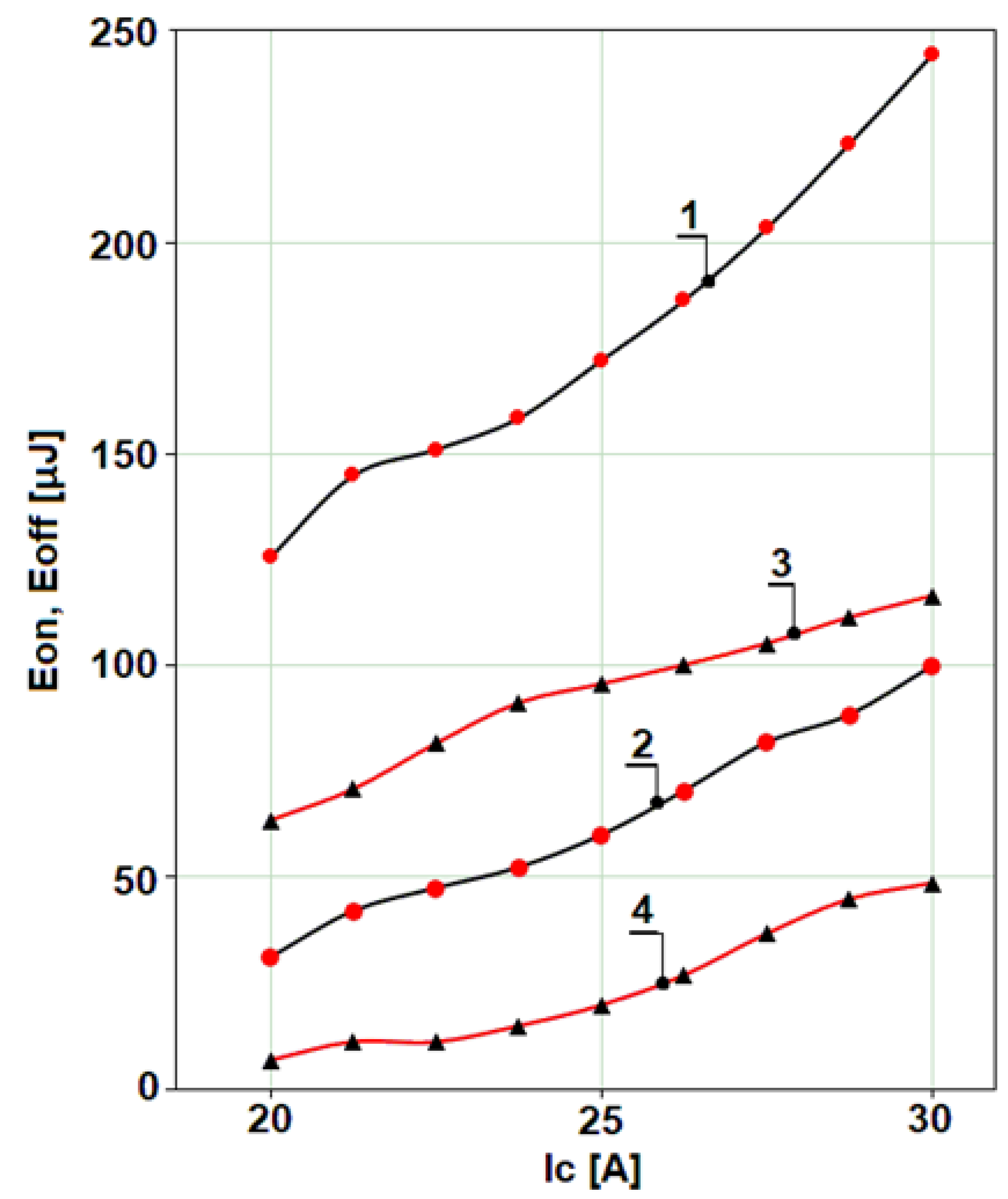
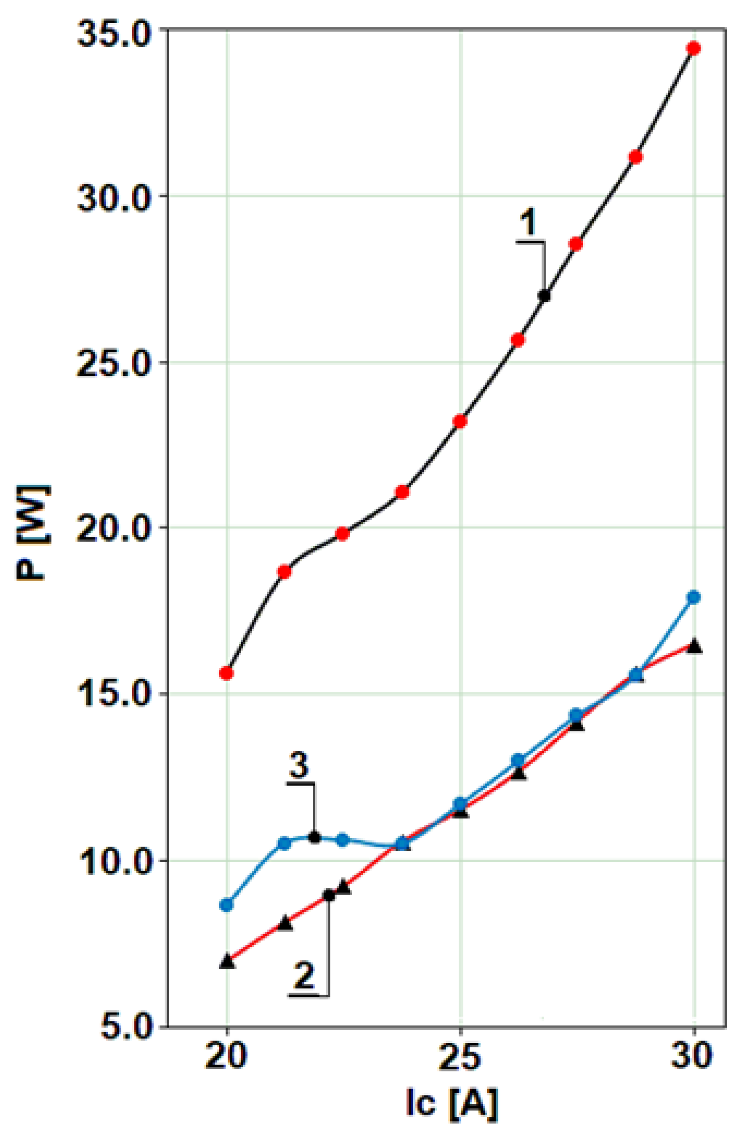
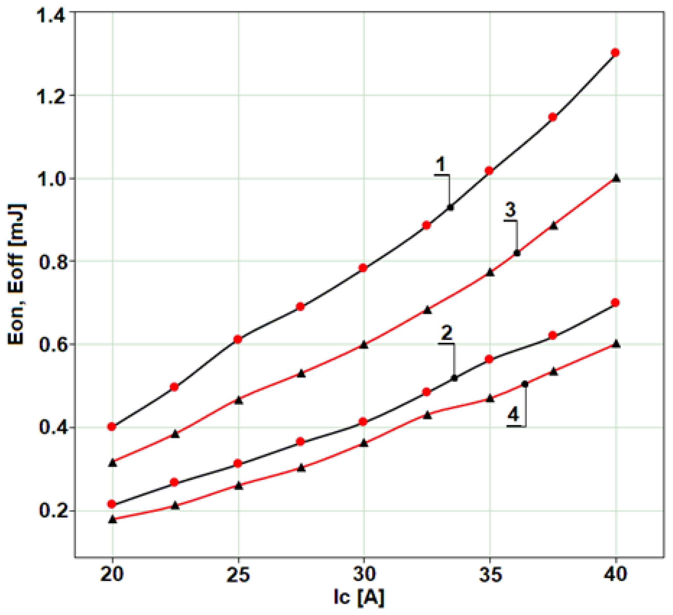
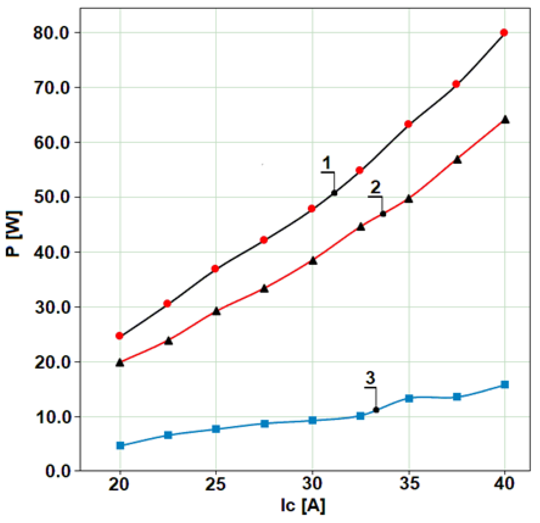
The above equations are the basis for the 3-pin and 4-pin energy estimations. While leading manufacturers offer such comparisons based only on their products, this research aims at a broader range of data. Figure 3, Figure 4, Figure 5 and Figure 6 show the graphical representation of statistical data collected for multiple 4-pin MOSFETs (Figure 3 and Figure 4) and 4-pin IGBTs (Figure 5 and Figure 6) for the Kelvin-connected transistors, respectively, given in Appendix A Table A1 and Table A2. The above-presented equations are applied to the energies E O N and E O F F (Equations (13) and (14)) and the total power loss calculation (Equations (9)–(12)).
Generally, for Kelvin-connected MOSFETs, the average reduction in E O N is 47.9 % , and that for E O F F is 65.2 % , calculated for the current range of 20 30   A . For the same range, the power loss reduction varies between 8.6   W and 17.9   W (Figure 4, diagram 3), which gives a 12.5   W reduction. The results were calculated for both packages at a switching frequency of 100   k H z .
It must be clarified that the numerical comparison was conducted with hard-switching to demonstrate the benefits of 4-pin packages. In the ZVS operation, the expected loss for the LLC converter will be lower than that depicted in Table 1. In this case, the Kelvin-connected 4-pin package could benefit the LLC topology, as analysed in [1,2,3,4,5,6,7,8,9,10,11,12,13,14,15,16,17,18,19,20,21,22,23,24,25,26,27,28,29,30], through reduced gate-drive oscillations, improved efficiency due to the reduced timing, and consequently, a stable ZVS operation with reduced E r r , leading to lower body diode loss. These assumptions have been verified experimentally, as described in Section 5.
Similarly, the results for Kelvin-connected IGBTs’ E O N show an average reduction of 22.8 % , and the E O F F reduction is 14.8 % , calculated for the range of 20 40   A . The power loss reduction ranges between 4.6   W and 15.7   W , giving a 10   W average result. These results are calculated with a 40   k H z switching frequency, typical for an interleaved PFC-Boost converter.
The statistical results can be supported by concrete data for specific transistors; the main datasheet parameters of the two packages are compared in Table 1. The data presented for t d ( o n ) delay on, t r rise, t d ( o f f ) delay off, t f fall, and t r r reverse-recovery times determine the energy values E o n , E o f f , total energy E t o t , and reverse-recovery energy E r r . The comparison is visualised graphically in Figure 7 for MOSFETs and in Figure 8 for IGBTs. For the transistors considered, the total energy is reduced for the 4-pin Kelvin-connected package MOSFET by 78.2 % and, for an IGBT in the same package, by 25 % .
The results indicate that the lower energy loss for the Kelvin-connected package also reduces the junction temperature. Table 2 shows the thermal parameters for a model based on an equivalent circuit for junction temperature estimation under steady-state conditions (Equations (20)–(23)). Table 3 shows the power loss and junction temperature comparison calculated for certain conditions. The applied thermal model shows a 4-pin MOSFET T j reduction of 22.1 % and 4-pin KE IGBT T j reduction of 17.8 % . The total power loss P t o t is calculated as a sum of the switching P O N (Equation (11)) and P O F F (Equation (12)) loss, and the conduction loss is
P c o n d = I D 2 × R o n
where I D is the average drain current, and R o n is the drain-to-source on-state resistance.
Table 2. Thermal model equivalent circuit and base equations.
PackageEquivalent CircuitEquation
Electricity 05 00034 i001Electricity 05 00034 i002 P t o t —total power at the junction T j = ( P t o t × R t h 1 ) + T c (20)
T j —junction temperature
R t h 1 —junction-to-case thermal resistance
T c —case temperature T c = ( P t o t × R t h 2 ) + T h s (21)
R t h 2 —case-to-heat-sink th. resistance
T h s —heat sink temperature
R t h 3 —heat-sink-to-ambient th. resistance T h s = P t o t × R t h 3 + T a m b (22)
T a m b —ambient temperature
Total thermal balance T j = ( P t o t × R t h 1 + R t h 2 + R t h 3 ) + T a m b (23)
Table 3. Comparison of the power losses and temperatures of 3-pin and 4-pin MOSFETs and IGBTs.
MOSFETIGBTs
IMW65R015M2H
TO-247 3-pin
IMZA65R015M2H
TO-247 4-pin
STGW80H65DFB
TO-247 3-pin
STGW80H65DFB-4
TO-247 4-pin
Datasheet data
R t h 1 (°C/W)
(datasheet)
0.440.32
R t h 2 (°C/W)
(estimated)
11
R t h 3 (°C/W)
(heat sink selected)
1.51.5
Calculated results according to Table 2
P t o t (W) 27.518.436.427.4
T j (°C) 120.994.2142.8117.4
T h s (°C) 81.267.694.781.2

3. Design of LLC Converter

The half-bridge LLC converter (Figure 1) design procedure is based on First Harmonic Analysis (FHA), conducted according to the equivalent circuit in Figure 9 [31,32,33,34,35,36,37,38,39,40,41]. The components of the circuit are as follows: C r is the resonant capacitor; L r is the resonant inductor; L m is the magnetising inductance; C p is the parasitic capacitance referred from the transformer’s primary side and the PCB layout; and R a c is the reflected load resistance.

3.1. Methodology for LLC Converter Design Based on FHA

The methodology for LLC converter design consists of using the main equations to calculate values for the resonant tank and transformer and determine the parameters of the primary-side MOSFETs and secondary-side rectifiers.
In Figure 9, C P represents the sum of the parasitic drain–source capacitance C D S and parasitic capacitance of the transformer’s primary side, which are usually neglected in conventional design procedures. However, to describe the minimum dead time, C P should not be neglected, especially when high-voltage, high-power MOSFET transistors are used.
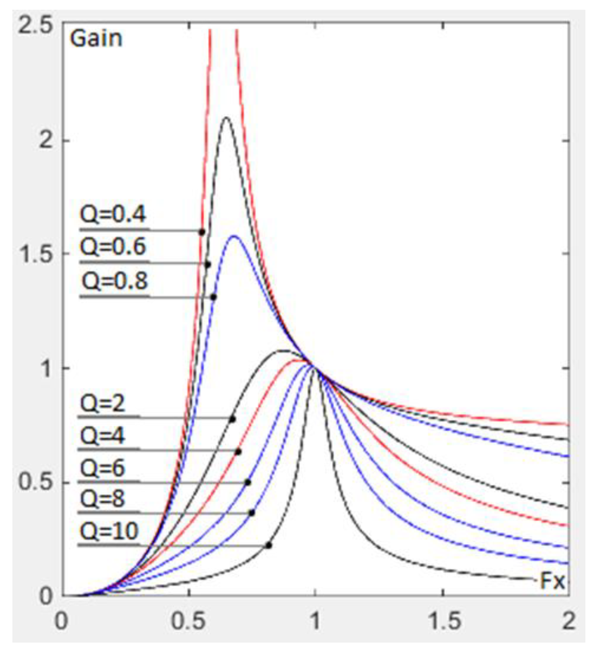
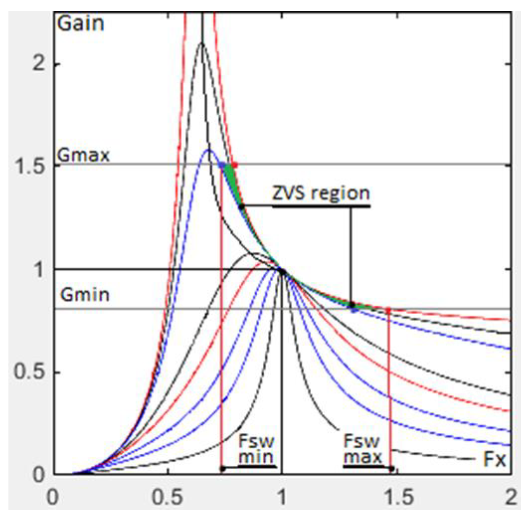
The LLC design methodology is given in Table 4, presenting the main equations applied to the converter design in Section 3.2. The gain G calculated (Equation (32)) versus the normalised frequency F x (Equation (26)) is depicted graphically in Figure 10. G   m i n and G m a x are depicted in Figure 11. The gain range determines the switching frequency range. As a product of this, the ZVS region on the primary side is specified, as shown in the exact figure.
Table 4. A design procedure of the LLC DC-DC converter.
DescriptionEquationNumber
Gain ( G ) G Q , m , F x = V o V i n = F x 2 ( m 1 ) ( m . F x 2 1 ) 2 + F x 2 . ( F x 2 1 ) 2 . ( m 1 ) 2 . Q 2 (24)
Quality factor (Q) Q = L r / C r R a c (25)
Normalised frequency ( F x ) F x = F s w F r (26)
Resonant factor ( m ) m = L p L r = L r + L m L r
where L p is the primary inductance, and L r is the resonant inductance
(27)
Reflected load resistance ( R 0 ) R a c = 8 π 2 . N p r i 2 N s e c 2 . R 0 (28)
Resonant capacitor C r C r = 1 2 π Q × F r × R a c (29)
Resonant inductance L r L r = 1 2 π F r 2 × C r (30)
Transient function G ( j ω ) G ( j ω ) = V o u t ( j ω ) V i n ( j ω ) (31)
Gain ( G ) including C p G ( j ω ) = j ω 2 j ω 4 L m C p   m + j ω 3 L m m .   R ac + j ω 2 C p L m k r 2 m + 1 m + 1 + j ω   L m k r 2 m   R ac + k r 2 m  
where ω = 2 π f ; k r = 1 / L r . C r
(32)
ZVS condition L m + L r . I m p k 2 2 2 . C p . V i n 2 2 (33)
Required minimum gain ( G m i n ) G   m i n = N t r . ( V o u t   m i n + V f ) V i n   m a x / 2 (34)
Required maximum gain ( G m a x ) G   m a x = N t r . ( V o u t   m a x + V f ) V i n   m i n / 2
where V f is the voltage drop over the diodes D r 1 and D r 2
(35)
Input LLC power ( P i n _ l l c ) P i n _ l l c = P o u t η l l c (36)
Minimum input voltage ( V i n _ m i n ) V i n _ m i n = V o u t _ p f c 2 2 P i n _ l l c × t h o l d _ u p C o u t (37)
Primary-side turns ( N p r i _ m i n ) N p r i _ m i n = N t r ( V o u t + V f ) 2 f S W m i n × G × B × A e (38)
Transformer turns ratio ( N t r ) N t r = N p r i N s e c (39)
RMS primary side ( I C r R M S ) I C r ( R M S ) = 1 η π I o u t 2 2 N t r 2 + N t r V o u t + V f 4 2 f r G L p L r 2 (40)
RMS current through each MOSFET ( I d _ r m s ) I d _ r m s = π 4 × I o u t (41)

3.2. LLC DC-DC Converter Design Case Study

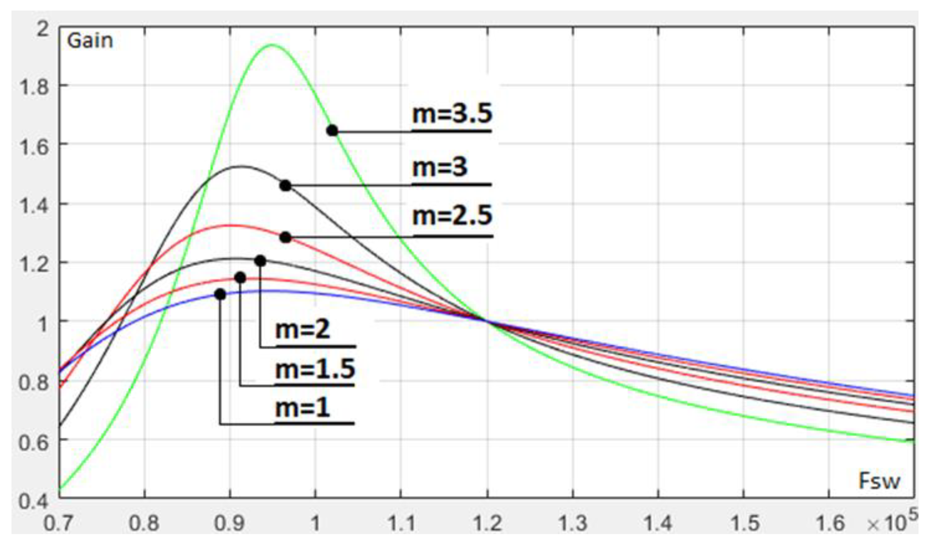
The foregoing LLC design methodology (Equations (24)–(41)) is for the converter design as a part of the overall battery charger (Figure 1). The transistor’s power loss is considered with ZVS conditions (Equations (15)–(18)) calculated for a Kelvin-connected 4-pin MOSFET. The LLC DC-DC converter design specification and results are presented in Table 5. Figure 12 shows the gain vs. the switching frequency for different resonant factors m (Equation (27)).
The transistor’s power loss under ZVS conditions (Equations (15)–(18)) at 3.6 kW output was evaluated for the selected Kelvin-connected 4-pin MOSFET. The results are as follows: Q G z v s = 110   n C , E O N z v s = 825   n J , E O F F z v s = 1032   n J , and E z v s = 1.857   µ J . The switching loss at a maximum operating frequency of 150   k H z will be 0.279   W . The conducting loss is calculated at 12.74   W (Equation (19)), rounding the total loss to 13   W . Applying the equivalent model (Equations (20)–(23)), the expected temperature allocation will be T j = 78.2   W and T h s = 59.5   W with the suggested 1.5   C / W heat sink thermal resistance.

4. The Design of the PFC-Boost Converter

The interleaved PFC-Boost topology chosen (Figure 1) aims to distribute the losses amongst the three channels, reducing the stress on individual devices. The converter is based on 4-pin Kelvin-connected IGBTs.

4.1. Methodology for PFC-Boost Design

The input PFC power P i n _ p f c is determined from the required output PFC power P o u t _ p f c , considering the input LLC power calculated in (Equation (36)) P o u t _ p f c = P i n _ L L C :
P i n _ p f c = P o u t _ p f c η p f c
where η p f c is the estimated PFC-Boost converter efficiency.
The total output current I o u t _ p f c is
I o u t _ p f c = P o u t _ p f c V o u t _ p f c
where V o u t _ p f c is the output PFC-Boost voltage.
The current through each PFC-Boost channel, considering the number of channels, N c h , is given by
I p f c _ c h = P o u t _ p f c V o u t _ p f c × N c h
The duty cycle D p f c at the maximum output voltage V o u t _ p f c is calculated from the maximum input voltage V i n _ m a x :
D p f c = V o u t _ p f c 2 V i n _ m a x V o u t _ p f c
The current ripple Δ I b o o s t in the Boost inductor at the minimum input voltage, i.e., the worst-case conditions, depends on the duty cycle and the switching frequency as follows:
Δ I b o o s t = D p f c × V o u t _ p f c 2 V i n _ m i n V o u t _ p f c × 1 F s w
The average inductor current I a v g _ p f c is calculated at the minimum input voltage V i n _ m i n as follows:
I a v g _ p f c = 2 V o u t _ p f c V i n _ m i n × η p f c
The inductance of each PFC inductor L p f c must be calculated at a specified ripple factor K r f and switching frequency F s w :
L p f c = 2 V i n _ m i n K r f × I a v g _ p f c × V o u t _ p f c 2 V i n _ m i n V o u t _ p f c × 1 F s w
The peak inductor current I L p k applies to an inductor selection with no core saturation, calculated from
I L p k = I a v g _ p f c × 1 + K r f 2
For a maximum output voltage ripple V p f c _ r i p p , the minimum capacitance of the output capacitor C o u t is given by
C o u t > I o u t _ p f c 2 π F i n V p f c _ r i p p
where F i n is the input line frequency.

4.2. PFC-Boost Converter Design Case Study

The interleaved PFC-Boost converter is designed to match the LLC converter (Section 3.2), supplying the necessary input power of 3750   W , 400   V . The design results (Equations (42)–(50)) are given in Table 6.
Applying the analytical power loss model (Equations (1)–(14) and (19)) and the thermal model (Equations (20)–(23)), the results for the selected 4-pin Kelvin-connected IGBT are a conduction loss of 0.24   W , a switching loss of 22   W , a total loss of 22.24   W , a junction temperature of 102.73   ° C , and a heat sink temperature of 95.61   ° C . As a comparison, the same IGBT with a standard 3-pin connection, based on the data in Table 1, shows a total loss of 31.24   W in the same application, leading to a junction temperature of 128.1   ° C and a heat sink temperature of 118.1   ° C . The total power loss dissipated from the three interleaved IGBTs is 93.7   W for the 3-pin package and 66.7   W for the Kelvin-connected package. Although both packages show satisfactory results, the power loss reduction of 27   W , or 28.8 % , shows that 4-pin discrete IGBTs could be preferred for this application.
Further significant power loss reduction could be achieved by applying CoolSiC 4-pin Kelvin-connected MOSFETs. Using the data in Table 1, the standard 3-pin package shows a power loss of 11.1   W and a junction temperature of 72.6 °C, while the 4-pin package dissipates 7.46   W and has a temperature of 61.9 °C. The results show that this approach would allow the interleaved Boost-PFC converter to be completed with only two transistors and a reduced heat sink size for power density improvement. In this case, the Boost PFC was reconstructed with two interleaved MOSFETS (Figure 13A). The comparison of 3-pin (diagram 1) and 4-pin (diagram 2) power losses (Figure 13B) and temperatures (Figure 13C) was conducted with a switching frequency of 66   k H z , according to the ASIC utilised, and a heat sink of 5.5   C / W , leading to power density improvement.

5. Experimental Setup

The experimental verification started with testing both packages, 3-pin and 4-pin TO-247, as individual switches, as shown in Figure 2, under the same conditions. The experiments were conducted with standard laboratory equipment, such as a Keysight DSOX1204G oscilloscope, an HMC8015 Rohde & Schwarz power analyser, a power supply, and digital multimeters. The experiments were conducted with both Boost-PFC and LLC converters and the entire battery charger (Figure 1). The measurements were taken for input/output power, efficiency, power loss, transistor junctions, gate driver control signals, and transistor temperature. The converters were tested under nominal and worst-case conditions, applying maximum power at minimum input voltage.
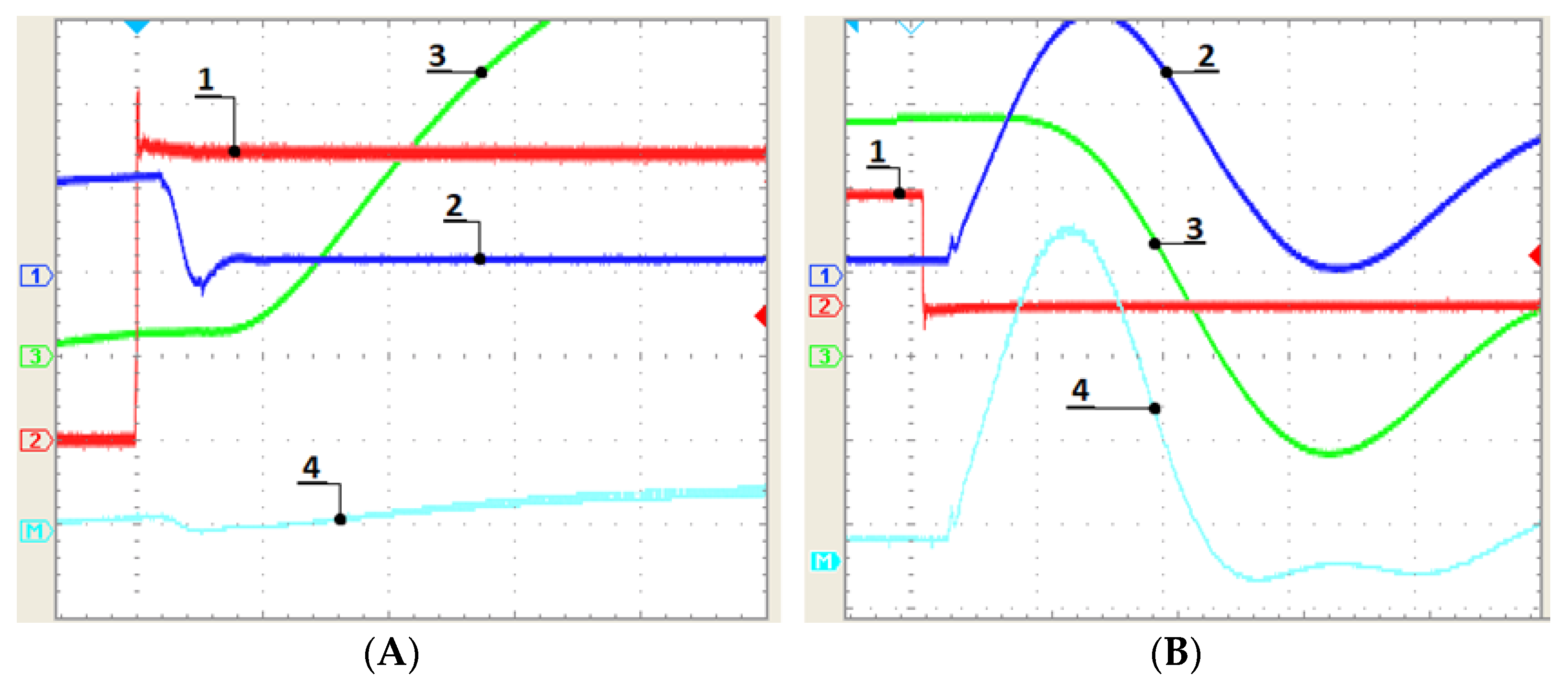
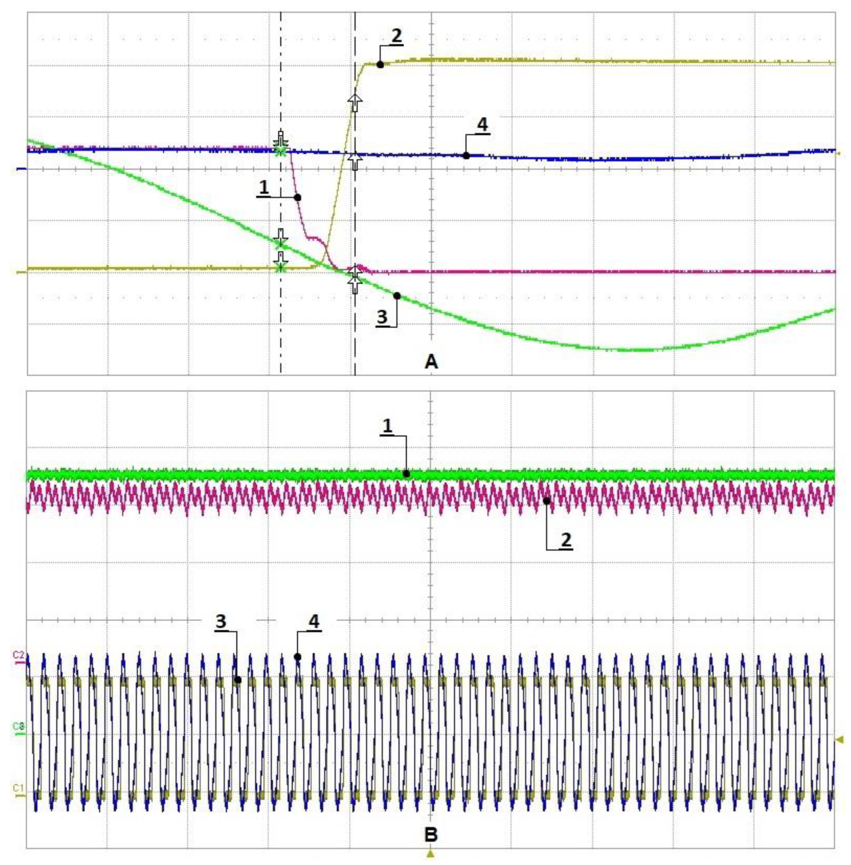
Oscillograms for the 3-pin results are depicted for switch-on (Figure 14A) and switch-off (Figure 14B) as follows: Trace 1 shows the PWM; 2 is the collector–emitter voltage; 3 is the collector current; and 4 is the result of using the mathematical function for power calculation, multiplying the current and voltage, embedded in the oscilloscope. The experiments were conducted with IGBT STGW80H65DFB-4 at a switching frequency of 40 kHz, according to the Boost PFC specified in Table 6.
A comparison of the oscillations in the gate-drive circuit is shown in Figure 15. The voltage over V L s (Figure 2A) during the 3-pin package switched-on process is shown in Figure 15A, and the voltage over V L g s (Figure 2B) for the 4-pin package is given in Figure 15B. It must be clarified that the result strongly depends on the board layout.
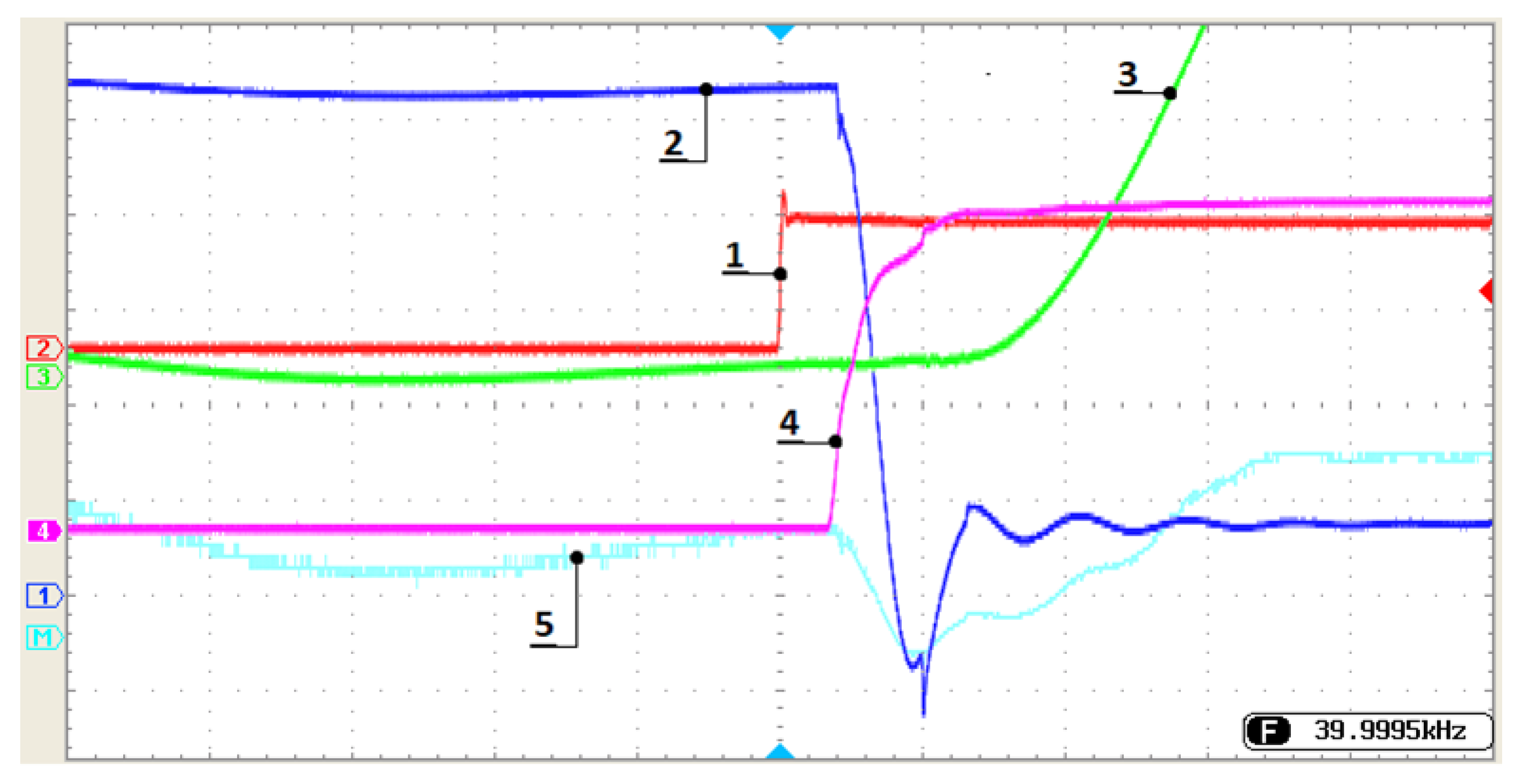
As a continuation of the previous experiment, the voltage applied to the gate is depicted in Figure 16 with diagram 4. The measurement shows the minimal impact of the Miller plateau for the 4-pin package.
The automotive battery charger has been prototyped and experimentally tested to support the analytical data and the design procedures. Both converter stages were initially tested in general, depicting their operation over the entire charger power range. Eventually, the integrated 4-pin Kelvin-connected operation was tested.
The PFC-Boost converter was tested according to the design described in Section 4.2. The results are presented as follows:
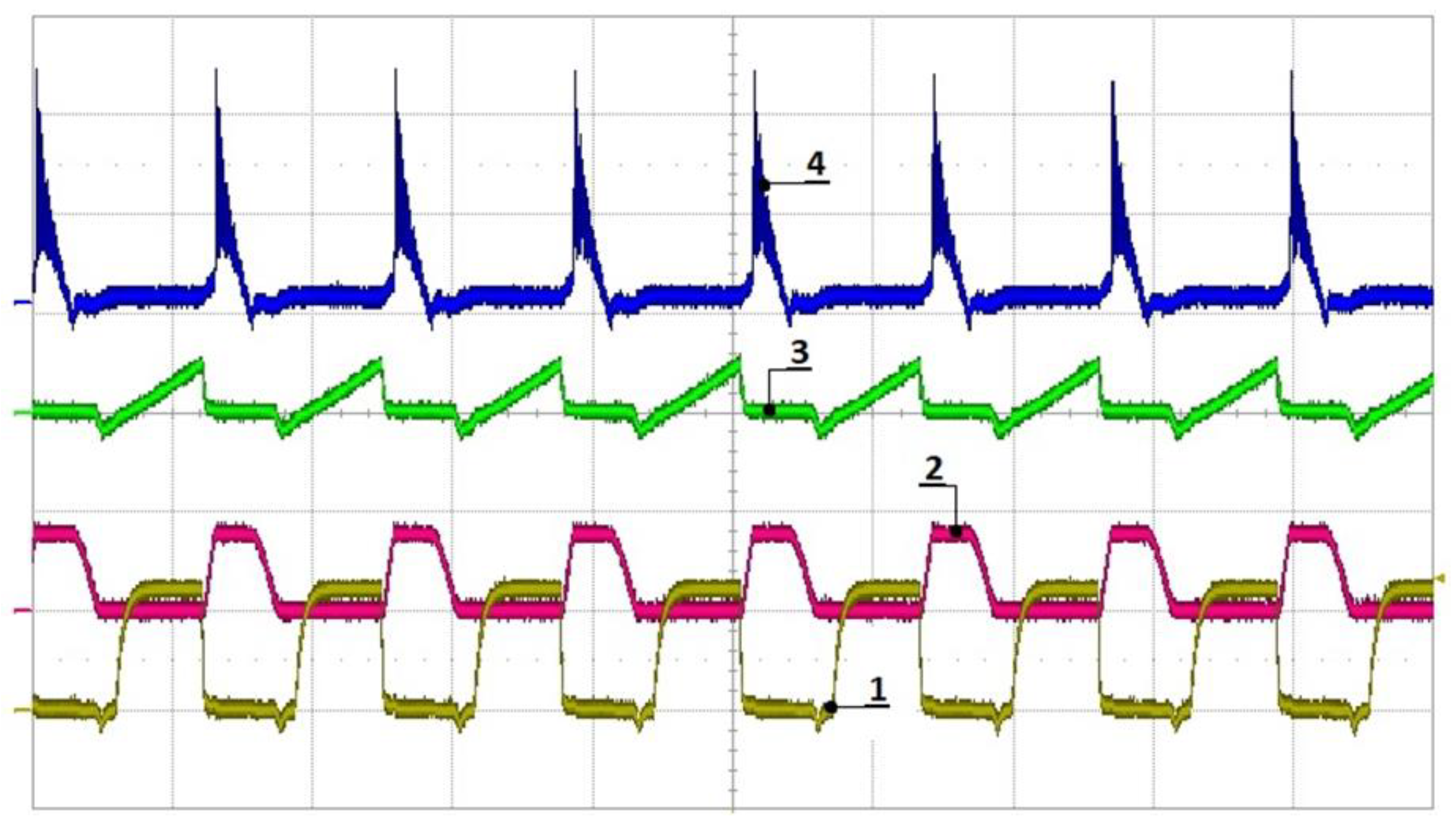
  • Figure 17 shows a single channel of the interleaved PFC-Boost converter implemented with three IGBTs, as suggested in the initial design (Table 6). The gate PWM (1) controls the switch with the collector-to-emitter voltage (2) and the collector current (3). The diode conducts the current in the OFF switch state (4).
  • Figure 18 shows the input PFC-Boost rectified DC voltage (1) without filtering. The PFC operates by varying the PWM (3) signal according to the input voltage variation and the collector-to-emitter voltage (2), leading to a stable output DC current (4).
  • Figure 19 shows the converter operating with the PFC at a nominal load (Figure 19A) and during the charger’s stand-by without the PFC (Figure 19B). The result demonstrates the ability of the converter to correct the power factor in the entire power range.
The LLC converter was tested first to show the ZVS operation with 4-pin Kelvin-connected transistors, according to Figure 1 and the design in the case study in Section 3.2, Table 5. The oscillograms present the following results:
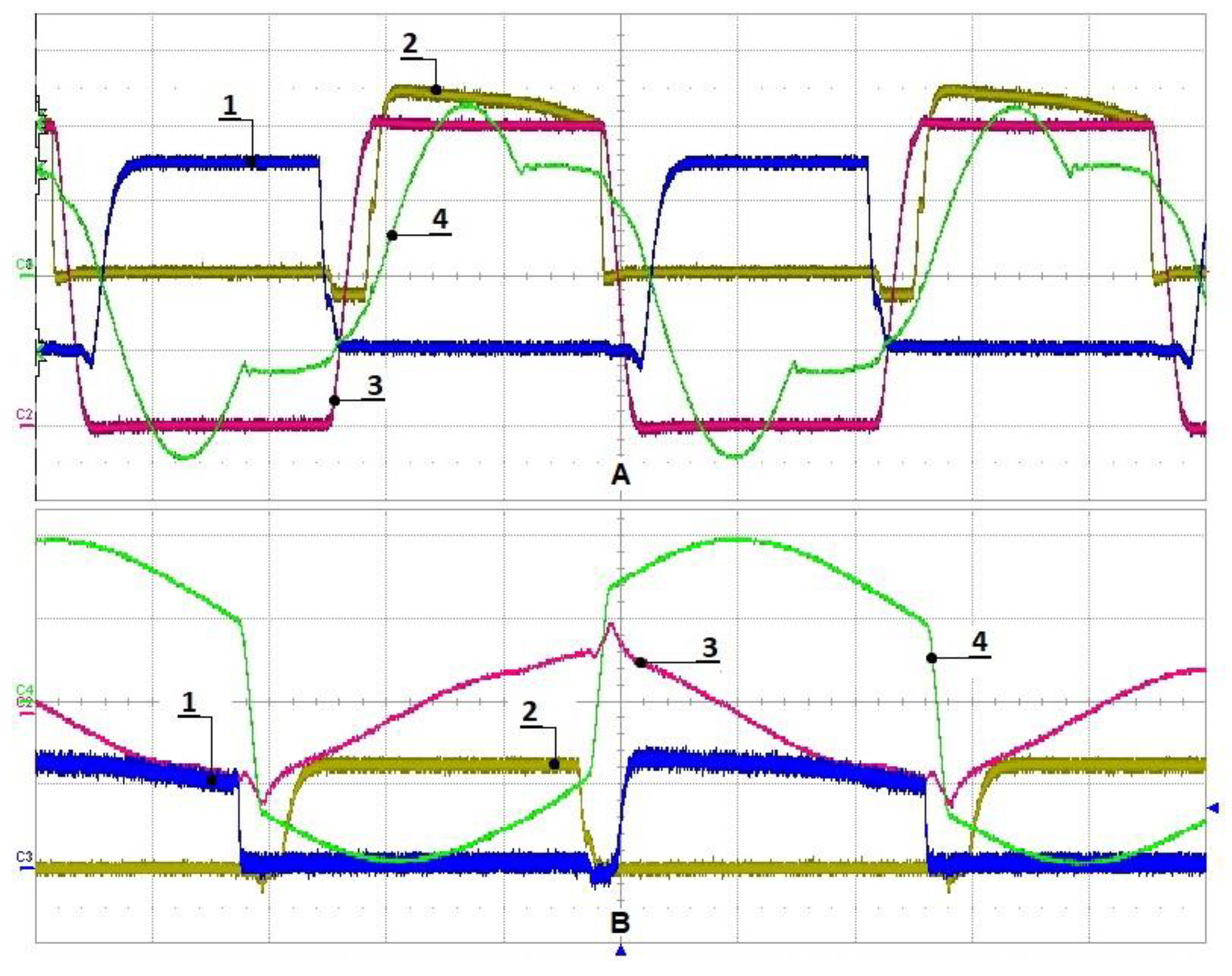
  • Figure 20A shows the ZVS operation in which the voltage at the middle point of the half-bridge (3) switches in the dead time between the two transistors’ PWM (1, 2). The current through the resonant capacitor and transformer (4) is depicted under the resonant frequency under output power control. Figure 20B shows the magnetising current (3) on the primary side. Both oscillograms depict the accurate operation of the LLC converter completed with 4-pin Kelvin-connected MOSFETs.
  • Figure 21A shows the ZVS in greater resolution, depicting the voltage switching at the zero point (3) between the drain-to-source voltages over the two MOSFETs (1, 2) in the half-bridge. The output DC current is shown in diagram 4. Figure 21B shows the output voltage (1) and current (2) in better resolution as part of the switching process. The output ripples are according to those accepted in the design procedure.
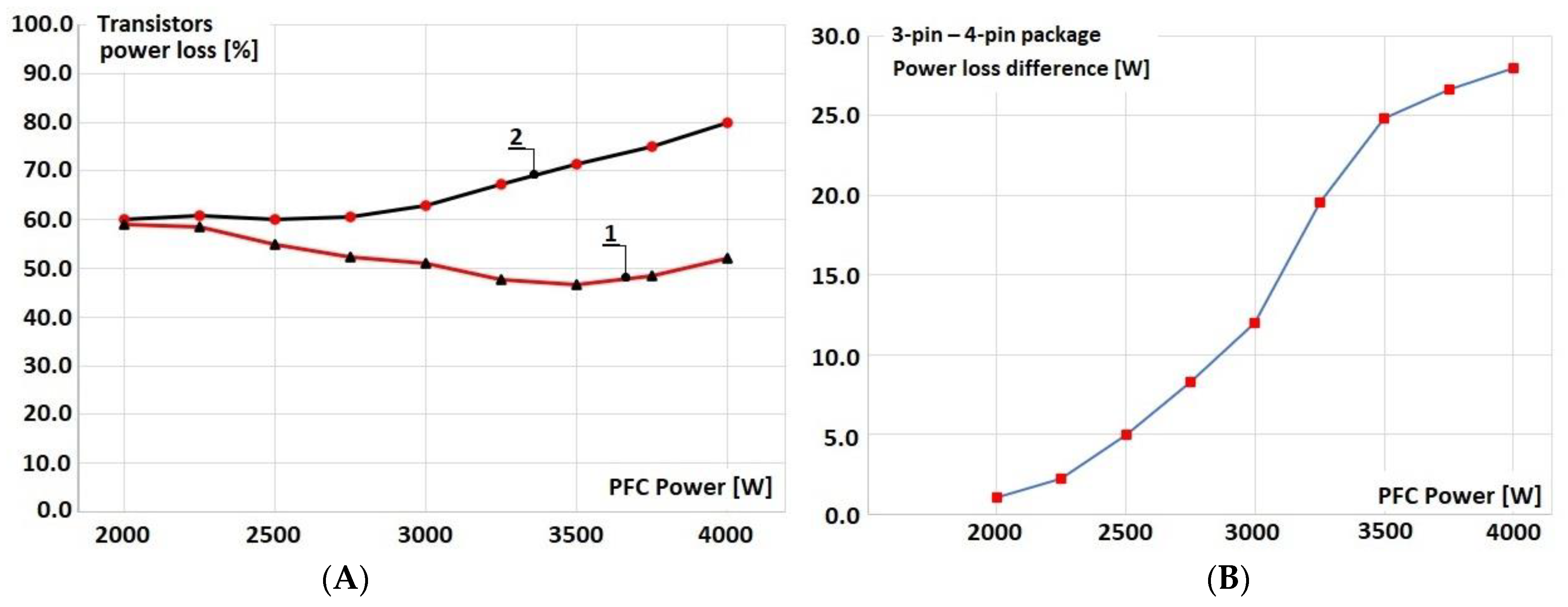
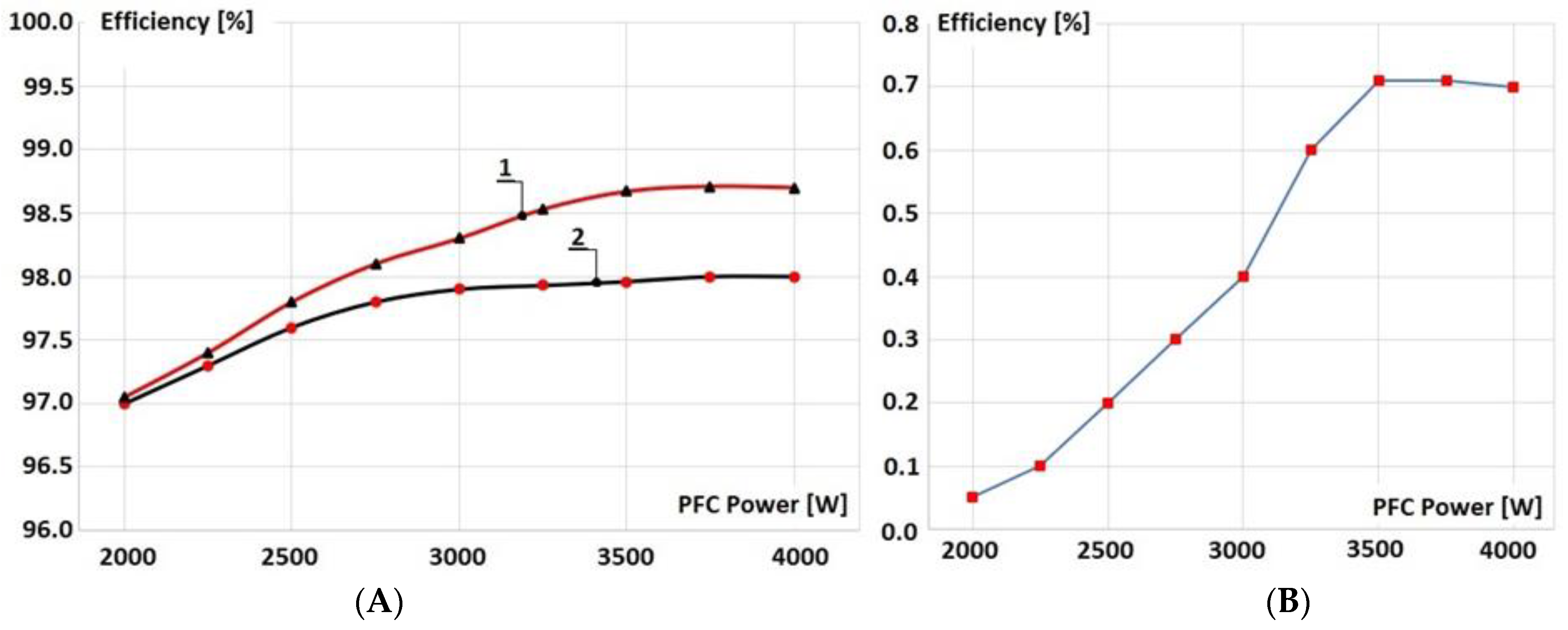
The energy efficiency of the Boost-PFC converter has been experimentally verified. Figure 22A compares the total transistors’ power loss, calculated from the measurement results over the entire power range. Diagram 1 shows the total loss of the three interleaved 4-pin Kelvin-connected IGBTs, and diagram 2 depicts the power loss of their 3-pin counterparts. The difference is shown in Figure 22B. As measured experimentally, the power loss reduction at the nominal rated power of 3750 W is 26.63 W or 8.9 W per transistor in this design. This contributes to a total efficiency improvement of 98% to 98.71% (Figure 23A) or 0.71% (Figure 23B) estimated for the interleaved transistors (Q1, Q2, and Q3, Figure 1).
Temperature rises were investigated using thermal imaging to confirm the power loss reductions. Images from both packages are compared in Figure 24: (A) 4-pin, showing 85.6 °C on the transistor cage, and (B) 3-pin, reaching 101.2 °C. The Kelvin-connected package connected to a heat sink for the presented experiments is shown in Figure 24C.
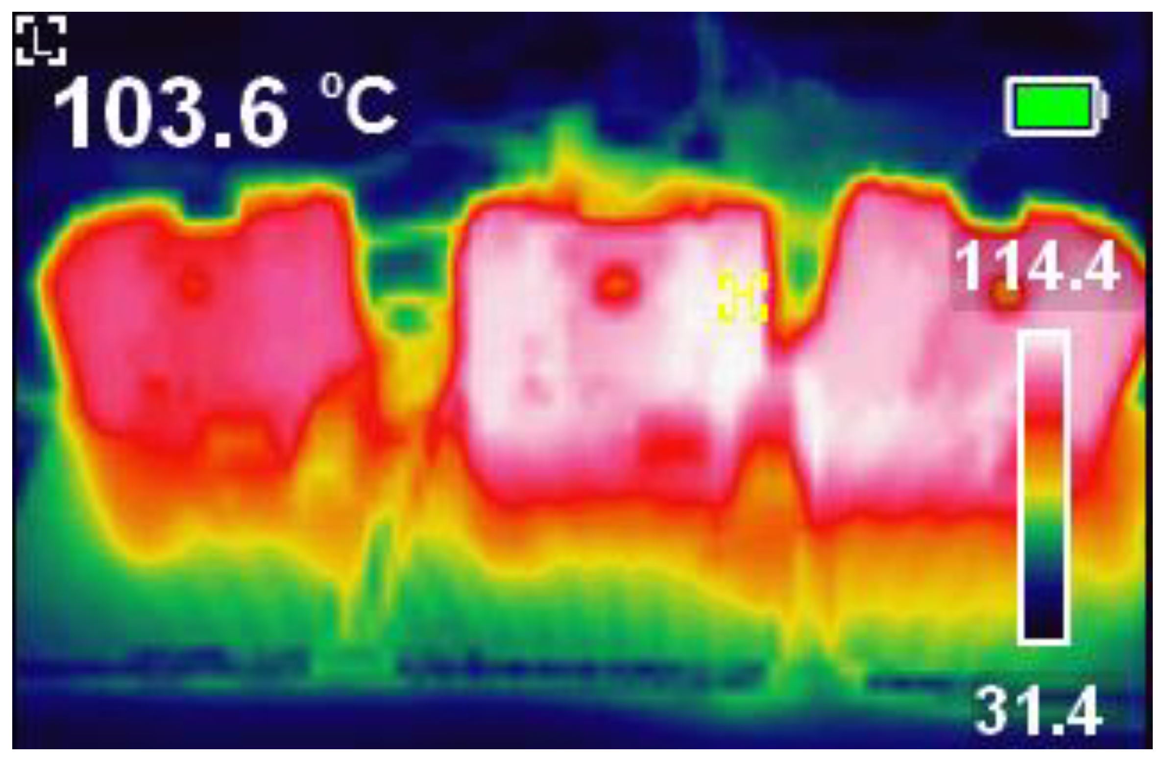
Figure 25 depicts a thermal image of the entire Boost-PFC power stage with three 4-pin TO-247 IGBTs. The final prototype is completed with heat sinks with a reduced surface, as suggested in the design above. The maximum temperature of the heat sink reaches 114.4 °C.
The LLC converter’s 4-pin MOSFET transistors’ thermal operation, according to the design in Section 3, is shown in Figure 26. The measured heat sink temperature is 53.5 °C versus the calculated temperature of 59.5 °C (Table 5).
The data obtained from the design and experimental measurements are summarised in Table 7. The results mismatch between the two studies is due to the 30% design safety margins applied to the datasheet parameters.
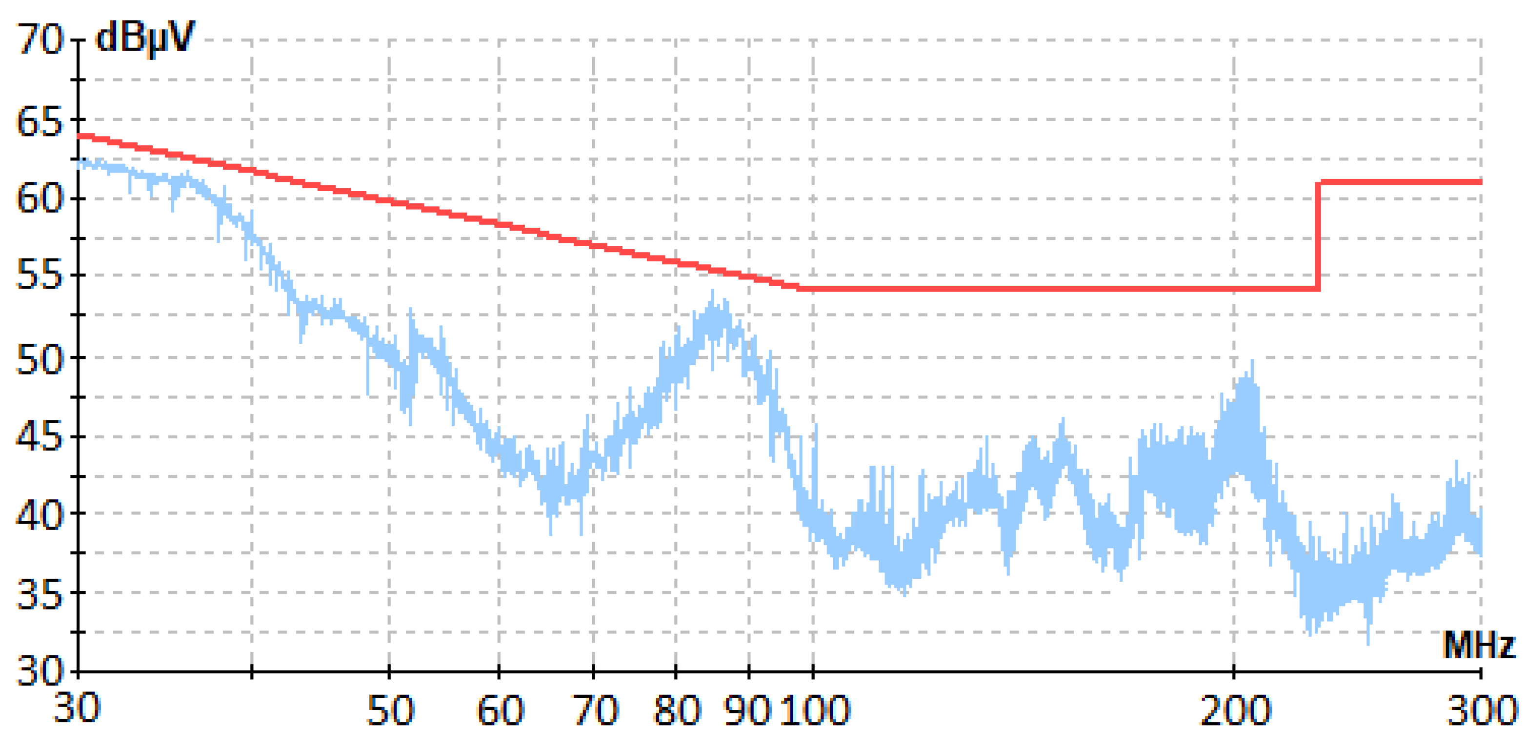
Finally, the Electromagnetic Interference (EMI), measured for the entire charger, is depicted in Figure 27. EMI improvement measures included the PCB design, specifically focused on the gate drivers, the parasitic element reduction enabled by the suggested switches, and proper grounding and shielding.

6. Results and Discussion

The results obtained in the conducted research can be summarised as follows:
  • The statistical data collected from multiple 4-pin Kelvin-connected and their 3-pin analogue TO-247 IGBTs and MOSFETs show a power loss reduction for the 4-pin package. The calculations were conducted using Equations (1)–(19) describing both packages’ power losses, and these are depicted graphically (Figure 3, Figure 4, Figure 5 and Figure 6) in the range 20–30 A, consistent with conditions in automotive onboard battery chargers. The results show that the expected power loss reduction obtained by applying Kelvin-connected transistors is between 8.6 W and 17.9 W.
  • The same calculations were applied to two specific IGBTs and MOSFETs (Table 1), including thermal models (Table 2) based on the equivalent circuits. The preliminary study shows that it can be expected that a 4-pin Kelvin-connected package offers a power loss reduction, leading to lower junction temperatures (Table 3). The results are obtained due to reduced ON and OFF switching times and, respectively, E o n and E o f f energies, for the Kelvin-connected transistors, as depicted in Figure 7 and Figure 8.
  • The 4-pin Kelvin-connected packages were successfully utilised in the design methodology of the Boost PFC (using IGBTs) and the resonant LLC converter (using MOSFETs). The case studies for both converters show that applying Kelvin-connected IGBTs to the interleaved Boost PFC reduces the switching loss. For the LLC converter, CoolSiC 4-pin MOSFETs can be recommended. The experimental study shows the stable operation of the Boost-PFC (Figure 17 and Figure 18) and LLC converters (Figure 20 and Figure 21).
  • The experimental study confirms the analytical results, showing a total power loss reduction of 26.63 W, or 8.9 W per transistor, for the three interleaved IGBTs in the Boost-PFC converter. The power loss reduction and efficiency improvement, experimentally depicted in Figure 23 and Figure 24, match the preliminary results presented in Section 2 and shown in Figure 3, Figure 4, Figure 5 and Figure 6.
  • Due to the power loss reduction, the heat sink temperature decreases proportionally from 101.2 °C to 85.6 °C, as the infrared images in Figure 22 show. Further temperature reductions, potentially leading to heat sink minimisation and power density improvement, could be achieved by applying SiC 4-pin MOSFET to the Boost-PFC converter (Figure 23 and Figure 24).
  • The experimental study also shows fewer gate circuit oscillations in both converters (Figure 15) and stable operation on the gate-drive circuits (Figure 14 and Figure 16). This result leads to acceptable EMI, as depicted in Figure 25.
Based on the presented results, it can be concluded that the 4-pin Kelvin-connected TO-247 transistors are a good candidate for further power loss reduction and efficiency improvement in power converters. In the presented research, such a result was demonstrated in the context of Boost-PFC and DC-DC LLC converters as a part of the automotive battery charger.

7. Conclusions

This research has conducted and presented analytical and experimental studies focused on the Kelvin-connected transistor package and its utilisation in the primary converters of a battery charger topology. The thorough literature review supported and defined the necessity of the presented results. The primary data obtained were used in the following design processes. The central battery charger converters, Boost PFC and DC-DC LLC, were designed with 4-pin Kelvin-connected TO-247 IGBT and MOSFET packages. Finally, the experimental results confirmed the expected power loss reduction and efficiency improvement. Furthermore, both converters showed stable operation with minimised oscillations, improved thermal operation, and power density improvement.

Author Contributions

Conceptualization, B.D. and R.M.; methodology, B.D.; validation, B.D. and R.M.; formal analysis, B.D. and R.M.; investigation, B.D. and R.M.; resources, B.D.; data curation, R.M.; writing—original draft preparation, B.D.; writing—review and editing, R.M.; visualization, B.D.; supervision, R.M. All authors have read and agreed to the published version of the manuscript.

Funding

This research received no external funding.

Data Availability Statement

Data are contained within the article.

Conflicts of Interest

The authors declare no conflicts of interest.

Appendix A

Table A1. IGBTs with the 4-pin Kelvin-source TO-247 package, used for the statistical analysis.
Infineon [60]ON Semiconductor [61]ST Microelectronics [62]
IPZA65R029CFD7; IPZA60R024P7FCH023N65S3L4stw48n60m2-4; stw56n60m2-4
IPZA60R016CM8; IPZ65R019C7FCH041N65EFL4stw56n65m2-4; stw57n65m5-4
IPZ60R017C7; IMZA65R030M1HNTH4L027N65S3Fstw65n023m9-4; stw68n60m6-4
IMZA65R027M1H; IMZA65R027M1HNTH4L040N65S3Fstw70n60dm6-4; stw70n60m2-4
IMZA65R020M2H; IMZA65R015M2HNVH4L040N65S3Fstw75n60m6-4; stw75n65dm6-4
Table A2. MOSFETs with Kelvin source TO-247 4pin, used for the statistical analysis.
Infineon [60]ON Semiconductor [61]ST Microelectronics [62]
IGZ50N65H5; IGZ75N65H5; IGZ100N65H5
IKZ50N65EH5; IKZ75N65EH5; IKZ75N65ES5
IKZA50N65EH7; IKZA75N65EH7; IKZA100N65EH7
FGH4L50T65MQDC50
FGH4L75T65MQDC50
FGH75T65SHDTL4
FGH75T65SQDNL4
FGHL50T65MQDTL4
FGHL75T65MQDTL4
STGW50H65DFB2-4
STGW60H65DFB-4
STGW75H65DFB2-4
STGW100H65FB2-4

References

  1. Wang, Y.; Zhao, D.; Ma, X.; Chen, B.; Chen, C. Accurate model and switching characteristics of SIC MOSFET power modules with Kelvin source package. In Proceedings of the 11th International Conference on Power Electronics, Machines and Drives (PEMD 2022), Newcastle, UK, 21–23 June 2022; pp. 680–684. [Google Scholar] [CrossRef]
  2. Rizzo, S.A.; Salerno, N. Actual Reasons Involving Turn-Off Losses Improvement with Increasing Load and Gate Resistance in MOSFETs Enhanced with Kelvin Source. IEEE Trans. Ind. Electron. 2024, 71, 369–379. [Google Scholar] [CrossRef]
  3. Cherif, O.M.; Nadji, B.; Tadjer, S.A.; Bencherif, H. An Analytical Approach for Evaluating Turn-On Switching Losses in SiC MOSFET with Kelvin Pin: Concept and Implementation. IEEE Trans. Electron Devices 2024, 71, 3116–3122. [Google Scholar] [CrossRef]
  4. Zhang, W.; Zhang, Z.; Wang, F.; Costinett, D.; Tolbert, L.; Blalock, B. Common source inductance introduced self-turn-on in MOSFET turn-off transient. In Proceedings of the 2017 IEEE Applied Power Electronics Conference and Exposition (APEC), Tampa, FL, USA, 26–30 March 2017; pp. 837–842. [Google Scholar]
  5. Zhang, X. Performance Evaluation of Different Freewheeling Device Implementations for SiC MOSFETs with Kelvin Source Connections. In Proceedings of the 2020 IEEE 9th International Power Electronics and Motion Control Conference (IPEMC2020-ECCE Asia), Nanjing, China, 29 November–2 December 2020; pp. 1–6. [Google Scholar] [CrossRef]
  6. Pu, S.; Yang, F.; Zhang, N.; Vankayalapati, B.T.; Akin, B. A Comparative Study on Reliability and Ruggedness of Kelvin and Non-Kelvin Packaged SiC Mosfets. IEEE Trans. Ind. Appl. 2022, 58, 3863–3874. [Google Scholar] [CrossRef]
  7. Mandal, M.; Roy, S.K.; Basu, K. Analytical Switching Transient Model of TO-247-4 Packaged SiC MOSFETs and Comparison with TO-247-3 Devices. In Proceedings of the 2022 IEEE Energy Conversion Congress and Exposition (ECCE), Detroit, MI, USA, 9–13 October 2022; pp. 1–8. [Google Scholar] [CrossRef]
  8. Yang, F.; Wang, Z.; Liang, Z.; Wang, F. Electrical Performance Advancement in SiC Power Module Package Design with Kelvin Drain Connection and Low Parasitic Inductance. IEEE J. Emerg. Sel. Top. Power Electron. 2019, 7, 84–98. [Google Scholar] [CrossRef]
  9. Chang, C.-W.; Spieler, M.; Burgos, R.; El-Refaie, A.; Dong, D. A Passive Balancing Method for Dynamic Current Sharing of Paralleled SiC MOSFETs with Kelvin-Source Connection. In Proceedings of the 2024 IEEE Applied Power Electronics Conference and Exposition (APEC), Long Beach, CA, USA, 11 July 2024; pp. 1589–1595. [Google Scholar]
  10. Ding, Y.; Mao, S.; Wang, Z.; Yang, S.; Li, W.; Zeng, K. A Review of the Crosstalk Suppression Methods for SiC MOSFETs in the Phase-leg Circuit Configuration. In Proceedings of the 2021 IEEE Workshop on Wide Bandgap Power Devices and Applications in Asia (WiPDA Asia), Wuhan, China, 25–27 August 2021; pp. 206–212. [Google Scholar] [CrossRef]
  11. Zhao, C.; Wang, L.; Zhang, F. Effect of Asymmetric Layout and Unequal Junction Temperature on Current Sharing of Paralleled SiC MOSFETs with Kelvin-Source Connection. IEEE Trans. Power Electron. 2020, 35, 7392–7404. [Google Scholar] [CrossRef]
  12. Xu, F.; Chen, L. Suppressing Gate Voltage Oscillation in Paralleled SiC MOSFETs for HEV/EV Traction Inverter Application. In Proceedings of the 2019 IEEE Energy Conversion Congress and Exposition (ECCE), Baltimore, MD, USA, 29 September–3 October 2019; pp. 3548–3553. [Google Scholar] [CrossRef]
  13. Baker, N.; Iannuzzo, F.; Li, H. Impact of Kelvin-Source Resistors on Current Sharing and Failure Detection in Multichip Power Modules. In Proceedings of the 2018 20th European Conference on Power Electronics and Applications (EPE’18 ECCE Europe), Riga, Latvia, 17–21 September 2018; pp. P.1–P.7. [Google Scholar]
  14. Xie, M.; Sun, P.; Ouyang, W.; Luo, Q.; Du, X. Online Monitoring Bond Wires Fault of SiC MOSFETs with Kelvin Package Based on Turn-on Source Voltage Ringing. IEEE Trans. Ind. Electron. 2024, 71, 9767–9776. [Google Scholar] [CrossRef]
  15. Sun, K.; Wang, J.; Burgos, R.; Boroyevich, D. Design, Analysis, and Discussion of Short Circuit and Overload Gate-Driver Dual-Protection Scheme for 1.2-kV, 400-A SiC MOSFET Modules. IEEE Trans. Power Electron. 2020, 35, 3054–3068. [Google Scholar] [CrossRef]
  16. Chen, J.; Jiang, X.; Li, Z.; Yu, H.; Wang, J.; Shen, Z.J. Investigation on Effects of Thermal Stress on SiC MOSFET Degradation through Power Cycling Tests. In Proceedings of the 2020 IEEE Applied Power Electronics Conference and Exposition (APEC), New Orleans, LA, USA, 15–19 March 2020; pp. 1106–1110. [Google Scholar]
  17. Smutka, J.; Scarpa, V.; Svetlik, J.; Hajek, J. Improvement of Dynamic Characteristics of discrete 1200V SiC MOSFETs through Kelvin Source connection. PCIM Europe Digital Days 2020. In Proceedings of the International Exhibition and Conference for Power Electronics, Intelligent Motion, Renewable Energy and Energy Management, Nuremberg, Germany, 6–18 November 2020; pp. 1–7. [Google Scholar]
  18. Xue, P.; Davari, P. The Trade-off of Switching Losses and EMI Generation for SiC MOSFET with Common Source and Kelvin Source Configurations. In Proceedings of the 2023 25th European Conference on Power Electronics and Applications (EPE’23 ECCE Europe), Aalborg, Denmark, 4–8 September 2023; pp. 1–8. [Google Scholar]
  19. Iwanaga, T.; Omori, H.; Sakamoto, K.; Morizane, T.; Matayoshi, H. A New Type of Kelvin-Source SiC-VMOSFET for a High-Power Single-Ended Wireless EV Charger. In Proceedings of the 2020 2nd International Conference on Electrical, Control and Instrumentation Engineering (ICECIE), Kuala Lumpur, Malaysia, 28 November 2020; pp. 1–6. [Google Scholar]
  20. Cacciato, M.; Giorgio, F.; Nardo, D.; Rizzo, S.A.; Salerno, N.; Scarcella, G.; Vinci, G. Analysis of the different impact of the external Gate Resistance in 3-lead and 4-lead SuperJunction MOSFETs. In Proceedings of the 2021 AEIT International Annual Conference (AEIT), Milan, Italy, 4–8 October 2021; pp. 1–6. [Google Scholar]
  21. Abbatelli, L.; Cacciato, M.; Paternostro, D.; Rizzo, S.A.; Scarcella, G.; Scelba, G. Performance Assessment of an Automotive-grade TO-247 IGBT copacked with SiC diode in a bidirectional buck converter. In Proceedings of the 2020 AEIT International Conference of Electrical and Electronic Technologies for Automotive (AEIT AUTOMOTIVE), Turin, Italy, 18–20 November 2020; pp. 1–5. [Google Scholar]
  22. Klobucar, B.; Yuan, Z. 1200V Discrete CoolSiC(TM) MOSFETs in a Comparison with the Trenchstop HighSpeed IGBTs for High-Speed Spindles and Servo Drive System. In Proceedings of the PCIM Europe Digital Days 2020; International Exhibition and Conference for Power Electronics, Intelligent Motion, Renewable Energy and Energy Management, Nuremberg, Germany, 7–8 July 2020; pp. 1–6. [Google Scholar]
  23. Rizzo, S.A.; Scelba, G.; Susinni, G.; Paternostro, D.; Scollo, R. Comparison between innovative TO-247 IGBT copacked with SiC diode and SiC MOSFET in bidirectional boost converter. In Proceedings of the 2020 2nd IEEE International Conference on Industrial Electronics for Sustainable Energy Systems (IESES), Cagliari, Italy, 1–3 September 2020; pp. 359–364. [Google Scholar]
  24. Sobe, K.; Engl, L.; Haque, N.U. Experimental analysis of the current-carrying capacity of discrete IGBTs in TO-247-based packages. PCIM Asia 2020. In Proceedings of the International Exhibition and Conference for Power Electronics, Intelligent Motion, Renewable Energy and Energy Management, Shanghai, China, 10 May 2020; pp. 1–6. [Google Scholar]
  25. Crisafulli, V. A new package with kelvin source connection for increasing power density in power electronics design. In Proceedings of the 2015 17th European Conference on Power Electronics and Applications (EPE’15 ECCE-Europe), Geneva, Switzerland, 8–10 September 2015; pp. 1–8. [Google Scholar] [CrossRef]
  26. Shen, S.; Sahan, B.; Jaeger, C.; Puyadena, A.; Brodt, A.; Lenze, A.; Mueller, C.R. Higher efficiency and power density of variable speed drives with new TRENCHSTOP(TM) IGBT7. PCIM Asia 2018. In Proceedings of the International Exhibition and Conference for Power Electronics, Intelligent Motion, Renewable Energy and Energy Management, Shanghai, China, 5–7 June 2018; pp. 1–6. [Google Scholar]
  27. Zhu, H.; Cheng, X.; Ng, W.T.; Xu, D.; Li, X.; Xia, Y. A Self-Adaptive Measurement System for IGBT Collector Current Using Package Parasitics. IEEE Trans. Ind. Electron. 2021, 68, 7545–7555. [Google Scholar] [CrossRef]
  28. Chen, Y.; Meng, F.; Zhu, A.; Li, W.; He, X. Chip Metallization Aging Monitoring with Induced Voltage veE between Kelvin and Power Emitter for High Power IGBT Modules. In Proceedings of the 2020 IEEE Energy Conversion Congress and Exposition (ECCE), Detroit, MI, USA, 11–15 October 2020; pp. 4012–4016. [Google Scholar] [CrossRef]
  29. Wu, Q.; Chen, Y.; Luo, H.; Zhang, J.; Li, W.; He, X.; Fujishima, N.; Nishio, H.; Sumida, H. Identification Method for Various Failure Modes with Shared Kelvin and Power Wires Configuration in IGBT Power Modules. In Proceedings of the 2022 International Power Electronics Conference (IPEC-Himeji 2022- ECCE Asia), Himeji, Japan, 15–19 May 2022; pp. 133–138. [Google Scholar] [CrossRef]
  30. Baker, N.; Dupont, L.; Beczkowski, S.M.; Iannuzzo, F. Proof-of-Concept for an On-Chip Kelvin-Emitter RTD Sensor for Junction Temperature Monitoring of IGBTs. In IEEE Transactions on Components, Packaging and Manufacturing Technology; IEEE: Piscataway, NJ, USA, 2024. [Google Scholar] [CrossRef]
  31. Huang, M.-S.; Hu, J.-C.; Hsu, W.-H.; Huang, C.-W.A. Three-Level LLC Resonant Converter with PFM and PWM Control for Battery Charging Application. In Proceedings of the 2023 IEEE International Future Energy Electronics Conference (IFEEC), Sydney, Australia, 20–23 November 2023; pp. 57–61. [Google Scholar] [CrossRef]
  32. Lin, P.; Zhu, Y.; Li, H.; Zhao, X. Design Methodology and Control Strategy of Phase shifted LLC Resonant Converter Based SiC MOSFET for Battery Charger of High-Speed Train. In Proceedings of the 2023 9th International Conference on Electrical Engineering, Control and Robotics (EECR), Wuhan, China, 24–26 February 2023; pp. 187–191. [Google Scholar] [CrossRef]
  33. Ditze, S.; Ehrlich, S.; Weitz, N.; Sauer, M.; Abmus, F.; Sacher, A.; Joffe, C.; Seßler, C.; Meibner, P. A High-Efficiency High-Power-Density SiC-Based Portable Charger for Electric Vehicles. Electronics 2022, 11, 1818. [Google Scholar] [CrossRef]
  34. Campanini, A.; Simonazzi, M.; Bosi, M.; Rossi, C. Design and Comparison between PSFB and LLC 400/48V DC/DC Stage for Onboard Battery Charger During Total and Partial CC-CV Charging Cycles. In Proceedings of the 2022 IEEE 21st Mediterranean Electrotechnical Conference (MELECON), Palermo, Italy, 14–16 June 2022; pp. 1102–1106. [Google Scholar]
  35. Alatai, S.; Salem, M.; Alhamrouni, I.; Ishak, D.; Bughneda, A.; Kamarol, M. Design Methodology and Analysis of Five-Level LLC Resonant Converter for Battery Chargers. Sustainability 2022, 14, 8255. [Google Scholar] [CrossRef]
  36. Kim, J.-Y.; Lee, B.-S.; Kwon, D.-H.; Lee, D.-W.; Kim, J.-K. Low Voltage Charging Technique for Electric Vehicles with 800 V Battery. IEEE Trans. Ind. Electron. 2020, 69, 7890–7896. [Google Scholar] [CrossRef]
  37. Shen, Y.; Zhao, W.; Chen, Z.; Cai, C. Full-Bridge LLC Resonant Converter with Series-Parallel Connected Transformers for Electric Vehicle Onboard Charger. IEEE Access 2018, 6, 13490–13500. [Google Scholar] [CrossRef]
  38. Shahzad, M.I.; Iqbal, S.; Taib, S. Interleaved LLC Converter with Cascaded Voltage-Doubler Rectifiers for Deeply Depleted PEV Battery Charging. IEEE Trans. Transp. Electrif. 2018, 4, 89–98. [Google Scholar] [CrossRef]
  39. Arshadi, S.A.; Ordonez, M.; Eberle, W.; Craciun, M.; Botting, C. Three-Phase LLC Battery Charger: Wide Regulation and Improved Light-Load Operation. IEEE Trans. Power Electron. 2021, 36, 1519–1531. [Google Scholar] [CrossRef]
  40. Tang, Y.; Kong, D.; Duan, C.; Sun, H. Optimal Design of LLC Resonant DC Transformer under Adaptive Frequency Tracking Strategy. Electronics 2020, 9, 2160. [Google Scholar] [CrossRef]
  41. Bae, J.; Resonance, Y. Characteristics of the LLC Resonant Half-Bridge Converter for the Rapid Charging of Personal Mobility Device Smart Batteries. Energies 2023, 16, 6538. [Google Scholar] [CrossRef]
  42. Ortiz-Castrillón, R.; Mejía-Ruíz, G.; Muñoz-Galeano, N.; López-Lezama, J.; Saldarriaga-Zuluaga, S. PFC Single-Phase AC/DC Boost Converters: Bridge, Semi-Bridgeless, and Bridgeless Topologies. Appl. Sci. 2021, 11, 7651. [Google Scholar] [CrossRef]
  43. Yeung, R.S.-C.; Fan, J.W.-T.; Chung, H.S.-H. A totem-pole PFC using hybrid pulse-width-modulation scheme. In Proceedings of the 2017 IEEE 3rd International Future Energy Electronics Conference and ECCE Asia (IFEEC 2017-ECCE Asia), Kaohsiung, Taiwan, 3–7 June 2017; pp. 1286–1290. [Google Scholar] [CrossRef]
  44. Do, N.-N.; Huang, B.-S.; Phan, N.-T.; Nguyen, T.-T.; Wu, J.-H.; Liu, Y.-C.; Chui, H.-J. Design and Implementation of a Control Method for GaN-Based Totem-Pole Boost-Type PFC Rectifier in Energy Storage Systems. Energies 2020, 13, 6297. [Google Scholar] [CrossRef]
  45. Kwak, B.; Kim, J. Digital Implementation Method for Synchronous PWM Control of GaN Transistor at Zero-Crossing of Totem-Pole PFC in Energy Storage Applications. Electronics 2021, 10, 30. [Google Scholar] [CrossRef]
  46. Qiqi, L.; Bangyin, L.; Shanxu, D. Simplified Analytical Model for Estimation of Switching Loss of Cascode GaN HEMTs in Totem-pole PFC Converters. Chin. J. Electr. Eng. 2019, 5, 1–9. [Google Scholar]
  47. Huang, Y.-Y.; Lai, Y.-S. Novel Efficiency Optimized Inductor Design for GaN-Based Totem-Pole PFC. In Proceedings of the 2022 IEEE 31st International Symposium on Industrial Electronics (ISIE), Anchorage, AK, USA, 1–3 June 2022; pp. 933–938. [Google Scholar] [CrossRef]
  48. Yu, D.; Xie, X.; Dong, H. An Error Amplifier Scheme to Reduce Compensation Capacitor for Boost PFC Converter. IEEE J. Emerg. Sel. Top. Power Electron. 2023, 11, 2816–2825. [Google Scholar] [CrossRef]
  49. Yao, K.; Liu, J.; Zhu, D.; Jin, Z. High Power Factor CRM Boost PFC Converter with Optimum Switching Frequency Variation Range Control Based on Variable Inductor. IEEE Trans. Power Electron. 2021, 36, 11019–11025. [Google Scholar] [CrossRef]
  50. Bendicks, A.; Peters, A.; Frei, S. FPGA-Based Active Cancellation of the EMI of a Boost Power Factor Correction (PFC) by Injecting Modulated Sine Waves. IEEE Lett. Electromagn. Compat. Pract. Appl. 2021, 3, 11–14. [Google Scholar] [CrossRef]
  51. Campos, H.M.V.D.B.; Soares, J.W.M.; Badin, A.A.; Cortez, D.F. Single-Phase Hybrid Switched-Capacitor PFC Boost Rectifier with Low Voltage Gain. IEEE Trans. Power Electron. 2023, 38, 968–976. [Google Scholar] [CrossRef]
  52. Babaei, A.; Kaffashan, I.; Abrishamifar, A. An Improved Threefold Interleaved PFC Circuit with Better Voltage Profile and Optimising Current-Sharing Method. IEEE Can. J. Electr. Comput. Eng. 2021, 44, 253–260. [Google Scholar] [CrossRef]
  53. Soares, J.W.M.; Badin, A.A. An Interleaved PFC Boost Converter with Soft Commutations and Voltage Follower Characteristics. IEEE Trans. Ind. Electron. 2022, 69, 6732–6740. [Google Scholar] [CrossRef]
  54. Gangavarapu, S.; Rathore, A.K. Analysis and Design of Interleaved DCM Buck–Boost Derived Three-Phase PFC Converter for MEA. IEEE Trans. Transp. Electrif. 2021, 7, 1954–1963. [Google Scholar] [CrossRef]
  55. Duan, M.; Sun, D.; Duan, J.; Sun, L.; Liu, Y. Interleaved Modulation Scheme with Optimised Phase Shifting for Double-Switch Buck-Boost Converter. IEEE Access 2021, 9, 55422–55435. [Google Scholar] [CrossRef]
  56. Yang, F.; Li, C.; Cao, Y.; Yao, K. Two-Phase Interleaved Boost PFC Converter with Coupled Inductor Under Single-Phase Operation. IEEE Trans. Power Electron. 2020, 35, 169–184. [Google Scholar] [CrossRef]
  57. Bousungnoen, P.; Pao-La-Or, P. A Single-Phase Integrated Battery Charger Simulation Compare Onboard Battery Charger with PFC Boost Converter and PSFB DC-DC Converter. In Proceedings of the 2023 International Electrical Engineering Congress (iEECON), Krabi, Thailand, 8–10 March 2023; pp. 163–168. [Google Scholar] [CrossRef]
  58. Mamun, K.A.; Islam, F.R.; Haque, R.; Chand, A.A.; Prasad, K.A.; Goundar, K.K.; Prakash, K.; Maharaj, S. Systematic Modeling and Analysis of Onboard Vehicle Integrated Novel Hybrid Renewable Energy System with Storage for Electric Vehicles. Sustainability 2022, 14, 2538. [Google Scholar] [CrossRef]
  59. Dimitrov, B.S. A Battery Cell Equalisation System Based on a Supercapacitors Tank and DC-DC Converters for Automotive Applications. World Electr. Veh. J. 2023, 14, 185. [Google Scholar] [CrossRef]
  60. Available online: https://www.infineon.com/ (accessed on 22 September 2024).
  61. Available online: https://www.onsemi.com/ (accessed on 22 September 2024).
  62. Available online: https://www.st.com/ (accessed on 22 September 2024).
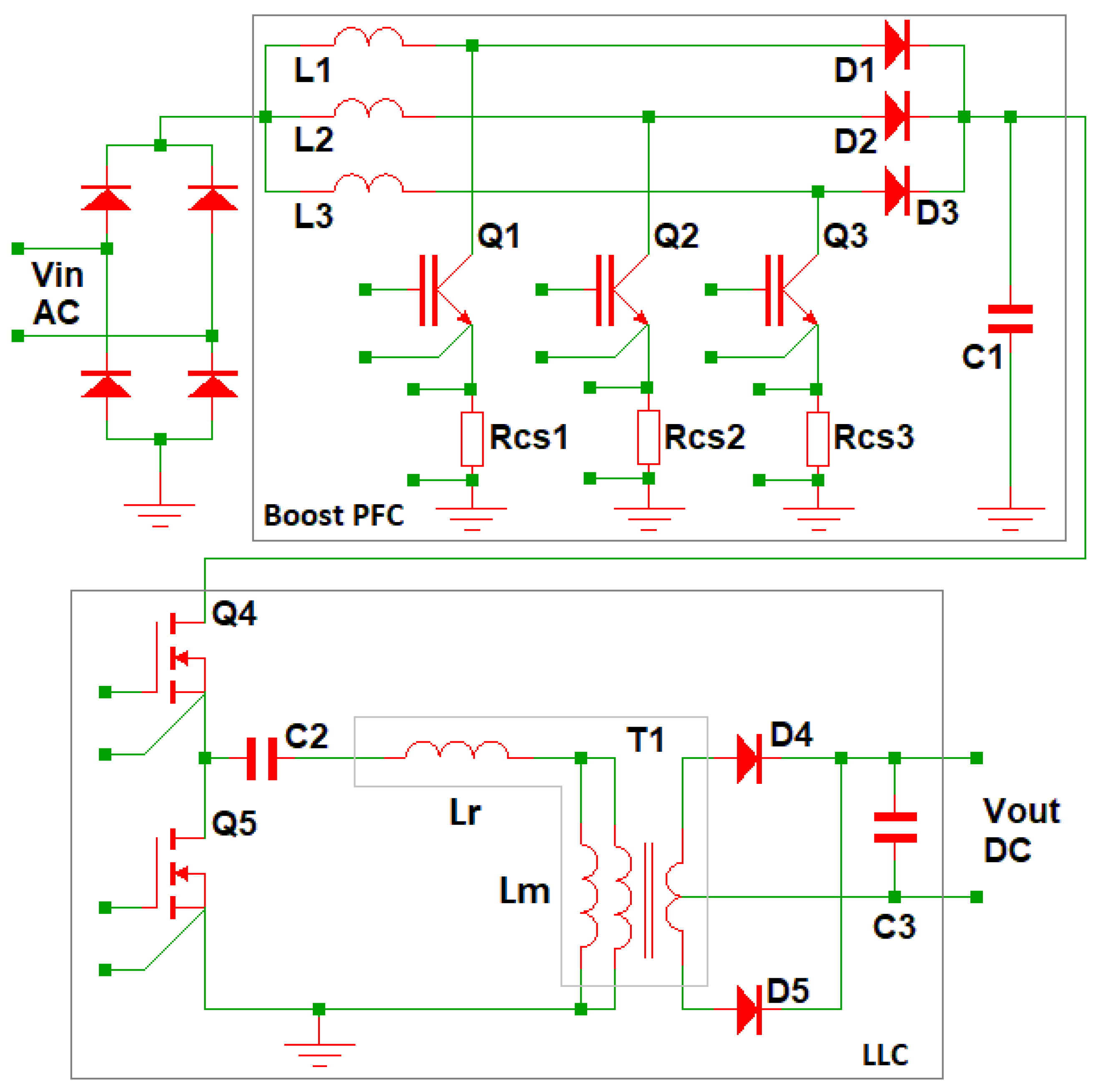
Figure 1. The central topology of the suggested battery charger with Kelvin-connected transistors.
Electricity 05 00034 g001
Figure 2. Primary circuits of TO-247 package with 3-pins (A) and Kelvin source 4-pins (B).
Electricity 05 00034 g002
Figure 3. Eon (1, 3) and E o f f (2, 4) energies calculated for MOSFETs TO-247 3-pin (1, 2) and TO-247 4-pin (3, 4) packages.
Electricity 05 00034 g003
Figure 4. Power losses calculated for MOSFETs TO-247 3-pin (1) and TO-247 4-pin (2) packages. Difference between the two packages’ power losses (3).
Electricity 05 00034 g004
Figure 5. Eon (1, 3) and Eoff (2, 4) energies calculated for IGBTs TO-247 3-pin (1, 2) and TO-247 4-pin (3, 4) packages.
Electricity 05 00034 g005
Figure 6. Power losses calculated for IGBTs TO-247 3-pin (1) and TO-247 4-pin (2) package. Difference between the power losses (3).
Electricity 05 00034 g006
Figure 7. Comparison between 3-pin (1—IMW65R015M2H) and 4-pin Kelvin-connected (2—IMZA65R015M2H) packages for the MOSFETs. The data are presented in Table 1.
Electricity 05 00034 g007
Figure 8. Comparison between 3-pin (1—STGW80H65DFB) and 4-pin Kelvin-connected (2—STGW80H65DFB-4) packages for the IGBTs. The data are presented in Table 1.
Electricity 05 00034 g008
Figure 9. Substitute resonance circuit for LLC converter design with FHA.
Electricity 05 00034 g009
Figure 10. A typical gain vs. normalised frequency diagram with different quality factors Q .
Electricity 05 00034 g010
Figure 11. Quality factor, normalised switching frequency range and zero-voltage switching (ZVS) regions.
Electricity 05 00034 g011
Figure 12. Gain vs. switching frequency with different resonant factors m .
Electricity 05 00034 g012
Figure 13. (A) Boost-PFC converter based on two interleaved SiC MOSFETs; (B) comparison between power losses; (C) temperature comparison between (1) 3-pin and (2) 4-pin packages.
Electricity 05 00034 g013
Figure 14. Experimental characteristics of 4-pin IGBT TO-247 package. (A) Turn-on and (B) turn-off processes. 1—PWM; 2—collector current; 3—collector–emitter voltage; 4—power calculation.
Electricity 05 00034 g014
Figure 15. Oscillations of the source inductances of (A) 3-pin and (B) 4-pin IGBT TO-247 packages. 1—PWM; 2—voltages over the straight inductances V L s and V L g s (Figure 2).
Electricity 05 00034 g015
Figure 16. Gate-drive characteristics of 4-pin IGBT TO-247 package. 1—PWM; 2—collector–emitter voltage; 3—collector current; 4—gate–emitter voltage; 5—math function for power calculation.
Electricity 05 00034 g016
Figure 17. Operation of PFC-Boost converter (single channel). (1) Gate PWM; (2) collector–emitter of IGBT transistor; (3) IGBT collector current; (4) diode current.
Electricity 05 00034 g017
Figure 18. Input PFC-Boost converter (single channel). (1) Input DC voltage; (2) collector–emitter voltage; (3) gate PWM; (4) output DC current.
Electricity 05 00034 g018
Figure 19. Input battery charger voltage (1) and current (2). Operation with PFC (A) and without PFC (B).
Electricity 05 00034 g019
Figure 20. LLC primary-side operation. (A) Below resonant frequency. (1) High-side MOSFET gate driver; (2) low-side MOSFET gate driver; (3) middle-point ZVS; (4) current through the resonant capacitor. (B) (1) High-side MOSFET gate driver; (2) low-side MOSFET gate driver; (3) magnetising current; (4) current through the resonant capacitor.
Electricity 05 00034 g020
Figure 21. LLC output voltage and current. (A) (1) Low-side gate drain-to-source voltage; (2) high-side drain-to-source voltage; (3) voltage over the resonant capacitor, ZVS; (4) secondary-side output current. (B) (1) Output voltage; (2) responses in the output current; (3) primary-side MOSFET switching; (4) primary-side voltage at the middle point at the resonant frequency.
Electricity 05 00034 g021
Figure 22. A comparison between the two packages. (A) The power loss of 4-pin (1) and 3-pin (2); (B) the power difference between the two packages, diagrams 1 and 2.
Electricity 05 00034 g022
Figure 23. The efficiency of the Boost PFC, estimated for the transistors Q1, Q2, and Q3, Figure 1: (A) 4-pin (2) and 3-pin (1); (B) the efficiency difference between diagrams 1 and 2.
Electricity 05 00034 g023
Figure 24. Thermal images of TO-247 (A) 4-pin Kelvin-connected and (B) 3-pin IGBTs; (C) 4-pin Kelvin-connected TO-247 package connected to a heat sink.
Electricity 05 00034 g024
Figure 25. Thermal image of the 4-pin IGBTs in the interleaved Boost PFC.
Electricity 05 00034 g025
Figure 26. Thermal image of the MOSFETs in the LLC converter.
Electricity 05 00034 g026
Figure 27. Electromagnetic Interference measured for the tested battery charger.
Electricity 05 00034 g027
Table 1. Comparison between the main parameters of 3-pin and 4-pin MOSFETs and IGBTs.
MOSFETIGBTs
IMW65R015M2H
TO-247 3-pin
IMZA65R015M2H
TO-247 4-pin
STGW80H65DFB
TO-247 3-pin
STGW80H65DFB-4
TO-247 4-pin
Times (ns)
t d ( o n ) 3411.68475
t r 2114.75235
t d ( o f f ) 2222280336
t f 86.43123
t r r 40.521.585112
Energies (µJ)
E o n 8258421001000
E o f f 19113815001700
E t o t 101622236002700
E r r 88.461.6257170
Table 5. LLC input data and design results.
Design Specification
Input ParametersOutput Parameters
Minimum voltage 350   V Minimum voltage 200   V
Nominal voltage 400   V Nominal voltage 300   V
Maximum voltage 420   V Maximum voltage 400   V
Estimated efficiency 0.96Output power 3600   W
Minimum switching frequency 75   k H z Nominal output current 12   A
Resonant frequency 100   k H z
Maximum switching frequency 150   k H z
Design parameters
Input power 3750   W Magnetising inductance 25.2   µ H
Transformer turns ratio 0.5Resonant inductance 6.4   µ H
Minimum gain 0.64Resonant capacitance 400   n F
Maximum gain 1.93Nominal resistance 5.1  
Quality factor 0.88Peak primary-side current 26.6   A
Resonant current 31.4   A Maximum output current 12.5   A
Magnetising current at minimum switching frequency 11.4   A Secondary half-wave current 8.8   A
Magnetising current at nominal switching frequency 8.5   A Energy accumulated in parasitic capacitors C d s in both transistors 88   µ J
Magnetising current at maximum switching frequency 5.6   A Dead time 33.3   n s
Selected semiconductors
Primary-side transistors: IMZA65R015M2H (CoolSiC™ 4-pin Kelvin-connected MOSFET)
Secondary-side rectifiers: VS-E5PH7506LHN3
Table 6. Interleaved PFC design results.
Design Specification
Input ParametersOutput Parameters
Minimum AC voltage 180   V Nominal output DC voltage 400   V
Maximum AC voltage 264   V Minimum output DC voltage 350   V
Line frequency 50   H z Output power 3750   W
Number of channels 3Output voltage ripples 0.05 %
Switching frequency 40   k H z
Efficiency (estimated) 92 %
Design parameters
Input power 4076.1   W Duty cycle 0.399
Nominal output DC current 9.4   A Inductor 130   µ H
Current per channel 3.1   A Inductor peak current at line brownout 160 V 21.3   A
Power per channel 1250   W Output capacitor 1500   µ F
Maximum switch current 5.2   A
Selected semiconductors
IGBT: STGW80H65DFB-4
Fast-recovery diode: VS-E5PH7506LHN3
Table 7. An experimental comparison between 3-pin and 4-pin IGBTs, with the TO-247 package, used for Boost-PFC design and prototyping.
3-pin IGBTs4-pin IGBTs
Total Loss for Three Interleaved PFC IGBTs (W)Total Loss per IGBT
(W)
Heat Sink/Junction Temperatures
(°C)
Total Loss for Three Interleaved PFC IGBTs (W)Loss per IGBT
(W)
Heat Sink/Junction Temperatures
(°C)
Calculated 93.731.24118.1/
128.1
66.622.295.61/
102.73
  • The total 4-pin package power loss reduction for 3 interleaved PFC IGBTs is 27.1 W.
  • The single-IGBT power loss reduction is 9.04 W.
Measured 7525101.2/
95.6
48.416.185.6/
78.5
  • The total 4-pin package power loss reduction for 3 interleaved PFC IGBTs is 26.63 W.
  • The single-IGBT power loss reduction is 8.9 W.
  • The junction temperatures are estimated according to package and heat sink temperatures.
Disclaimer/Publisher’s Note: The statements, opinions and data contained in all publications are solely those of the individual author(s) and contributor(s) and not of MDPI and/or the editor(s). MDPI and/or the editor(s) disclaim responsibility for any injury to people or property resulting from any ideas, methods, instructions or products referred to in the content.