Proceeding Paper

Physical Investigation of Spin-Coated MoS2 Films †

by
Grazia Giuseppina Politano
1,*,
Marco Castriota
1,2,*,
Maria Penelope De Santo
1,2,
Mario Michele Pipita
3,
Giovanni Desiderio
2,
Carlo Vena
1 and
Carlo Versace
1,2
1
Dipartimento di Fisica, Università della Calabria, 87036 Rende, CS, Italy
2
Licryl CNR/Nanotec c/o Dipartimento di Fisica, Università della Calabria, 87036 Rende, CS, Italy
3
Notredame s.r.l., c/o Dipartimento di Fisica, Università della Calabria, 87036 Rende, CS, Italy
*
Authors to whom correspondence should be addressed.
Presented at the 2nd International Online-Conference on Nanomaterials, 15–30 November 2020; Available online: https://iocn2020.sciforum.net/.
Mater. Proc. 2021, 4(1), 3; https://doi.org/10.3390/IOCN2020-08005
Published: 12 November 2020
(This article belongs to the Proceedings of The 2nd International Online-Conference on Nanomaterials)

Abstract

:
Among emerging Transition Metal Dichalcogenides (TMDCs), molybdenum disulfide (MoS2) has attracted a remarkable interest due to its many possible applications. In particular, MoS2 has potentialities not yet fully realized in solution-based applications. The morphological and the structural properties of MoS2 films deposited by spin-coating onto Si/SiO2 substrates were investigated by Scanning Electron Microscopy (SEM), Atomic Force Microscopy (AFM) and Micro-Raman Spectroscopy. High resolution AFM imaging highlights the presence of a layered structure. The thickness of each layer is estimated to be around 13 nm. Micro-Raman measurements reveal that there is a coexistence between 2H-MoS2 and 1T-MoS2 phases, which could be useful for electrical applications. Moreover, the band at 290 cm−1 is assigned to the amorphous phase of MoS2. The detectability of the mode E1g in back scattering geometry is ascribed to the disorder of the amorphous phase.

1. Introduction

Among Transition Metal Dichalcogenides (TMDCs), molybdenum disulfide (MoS2) offers several advantages because of its unique and tunable electronic properties. A simple model to describe the structure of MoS2 states that one molybdenum (Mo) atom is covalent bonded with three sulfur (S) atoms on the top and three S atoms on the bottom in a prismatic way. A layer is obtained when the prismatic structure is repeated infinite times on one plane. In this way, one layer is made by a plane of Mo atoms enclosed in two planes of S atoms [1]. While, the bonds among the different atoms inside a layer are covalent, the addition of others layers occurs by Van der Waals interactions, weaker than the former, among the different atoms of each layer [1]. MoS2 shows mainly two phases: One with a trigonal prismatic structure (2H-MoS2) and one with an octahedral structure (1T-MoS2). The two phases exhibit completely different electronic structures: 2H-MoS2 phase is semiconducting while 1T-MoS2 is metallic [2]. In [3], Eda et al. showed that 2H/1T hybrid structures coexist in chemically exfoliated MoS2 nanosheets.
Scalable production of two-dimensional (2D) materials can be achieved by solution-based exfoliation methods [4]. In particular, MoS2 has potentialities not yet fully realized in solution-based applications [5].
Scanning Electron Microscopy (SEM), Atomic Force Microscopy (AFM) and Micro-Raman spectroscopy measurements were carried out on MoS2 films spin-coated onto Si/SiO2 substrates.
Micro-Raman spectroscopy measurements reveal the coexistence of 2H-MoS2 and 1T-MoS2 phases, which is useful for electrical applications [6].

2. Materials and Methods

Silicon (Si) wafers, which are used as substrates, were ultrasonically cleaned in acetone, then in double-distilled water and isopropanol. At the end, they were dried with warm air.
The commercial aqueous solution of MoS2 dispersion 0.1–0.5 mg in H2O, which was obtained by solution-based exfoliation methods, was bought from Sigma Aldrich. The solution was sonicated for 30 min using an ultrasonic bath.
MoS2 films were reproducibly prepared by spin-coating the solution onto Si/SiO2 substrates (SiO2 thickness of ~2 nm). The results are reported on samples prepared at 6000 rpm spin coating speed and 60 s as deposition time.
The MoS2 flakes were characterized by scanning transmission electron microscope (STEM). A drop of the sample solution was placed on a Formvar/carbon on 300 gold mesh type S162A3 (Agar Scientific, UK) and dried at room temperature. SEM analysis was accomplished with a FEI Quanta FEG 400 F7 eSEM (Eindhoven, The Netherlands) microscope.
Tapping mode AFM images were obtained in ambient conditions with a Multimode 8 equipped with a Nanoscope V controller (Bruker Instruments, Santa Barbara, USA). Images were acquired using cantilevers with a force constant k = 5 Nm−1 (model TAP150A, Bruker, Santa Barbara, USA). The scan line speed was optimized between 1 and 3 Hz over 512 × 512 pixels. Image processing and analysis were carried out using the free software WSxM [7].
Micro-Raman spectra were collected by using a Horiba-Jobin Yvon (Darmstadt, Germany) microprobe apparatus (spectral resolution ∼2 cm−1), equipped with a Charge-Coupled Device (256 × 1024 pixels) detector cooled at −70 °C and with a 532 nm line of a diode laser, with an emitted power of 50 mW. The laser spot was about 2–3 µm of apparent diameter. The heating filters, with different optical densities, were used to avoid structural changes due to laser.

3. Results and Discussion

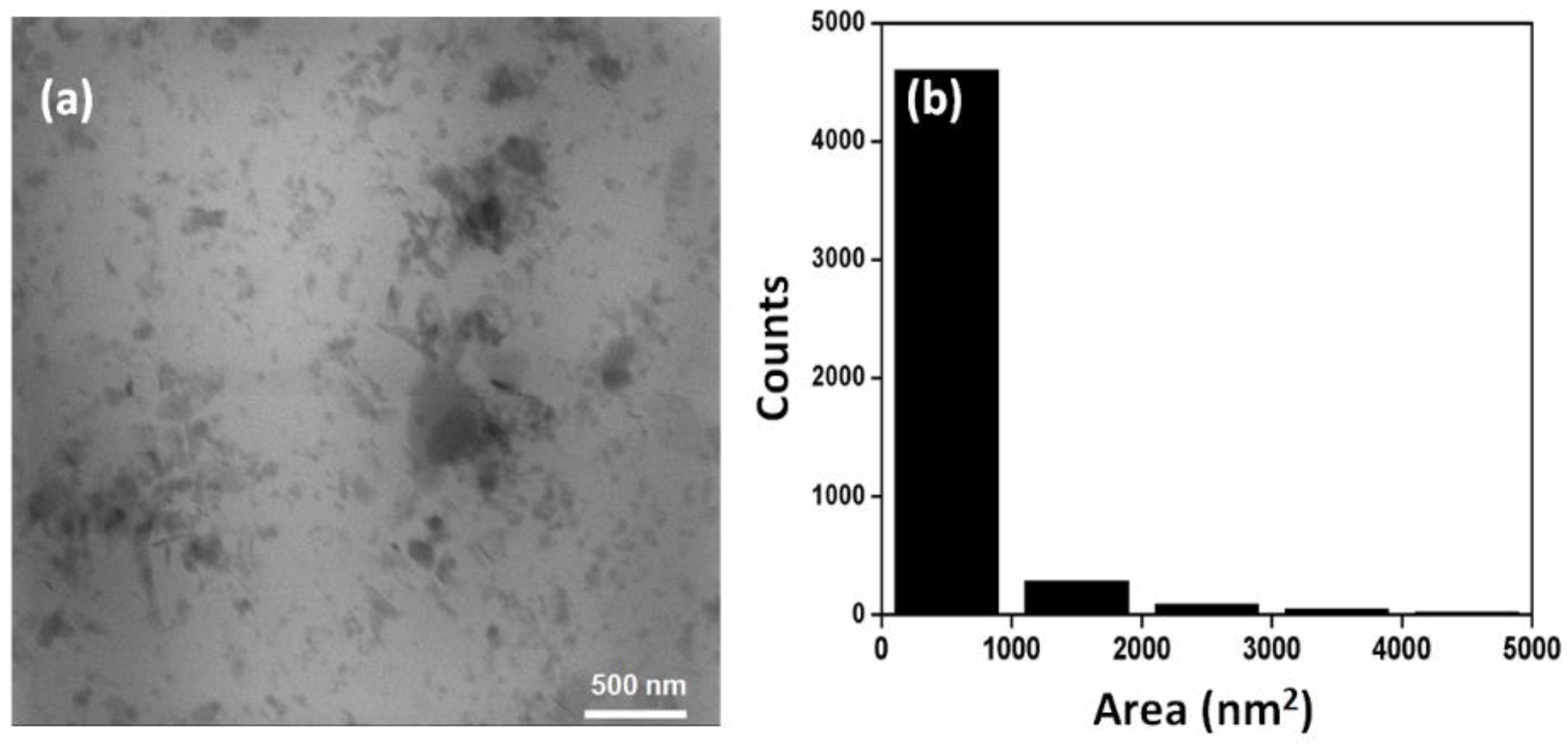
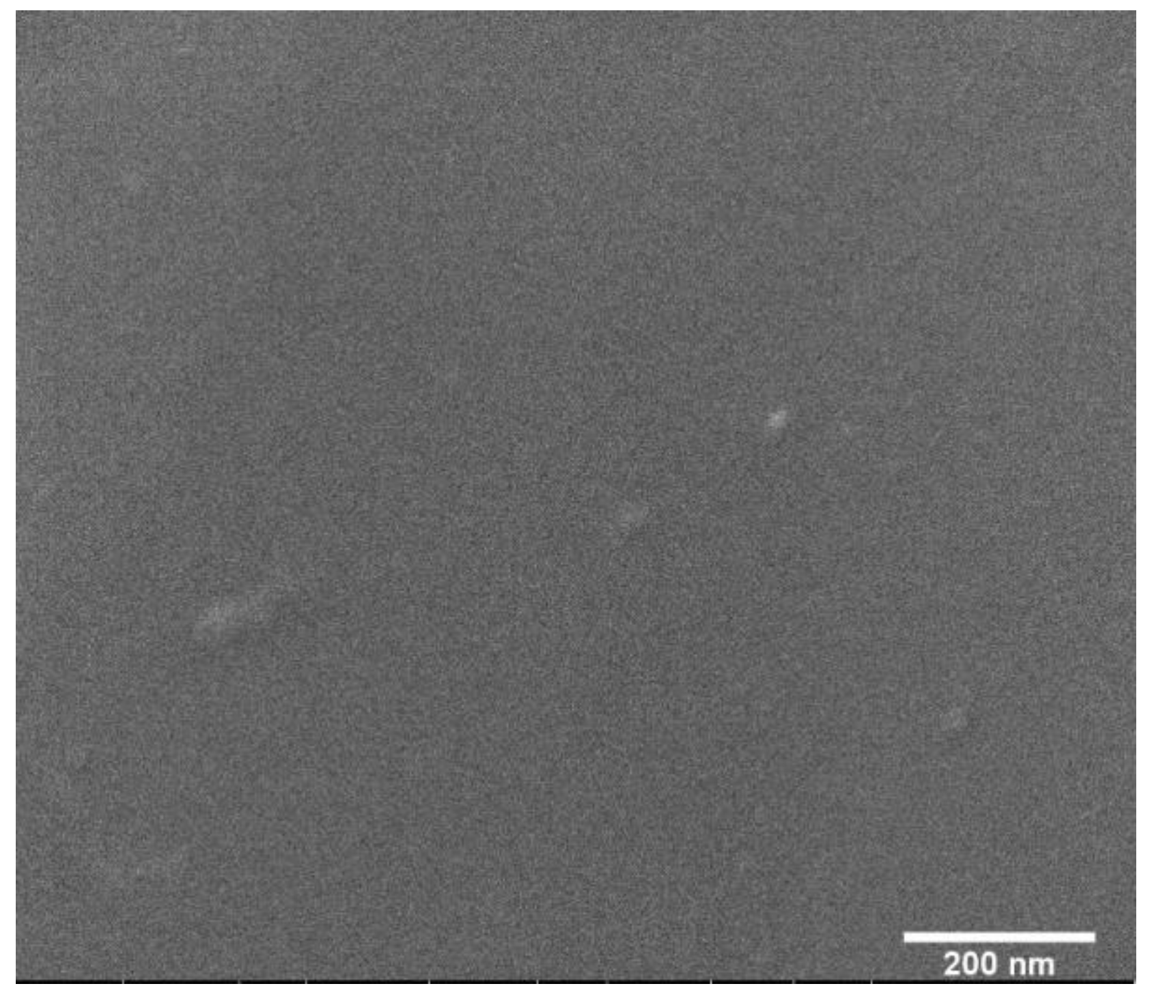
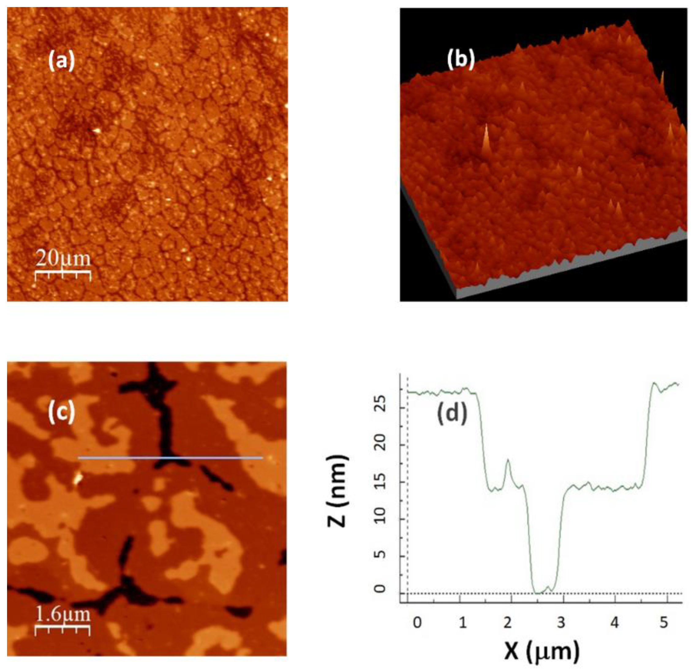
3.1. STEM, SEM and AFM Measurements

A STEM image of MoS2 flakes, drop-casted onto a gold mesh, is reported in Figure 1a.
The size distribution of the MoS2 flakes areas is shown in Figure 1b, by which it is evident that most MoS2 aggregates have dimensions less than 30 nm.
A SEM image of MoS2 films spin-coated onto Si/SiO2 substrate is reported in Figure 2.
The surface topographies of MoS2 films spin-coated onto Si/SiO2 substrates were characterized by AFM analysis. The investigated areas show a homogeneous MoS2 deposition on the surface as reported in Figure 3 in a 2D (a) and a three-dimensional (3D) representation (b). The root mean square roughness measured on 100 × 100 μm2 areas is (7.0 ± 1.5) nm. High resolution AFM imaging highlights the presence of a layered structure, visible in small areas in Figure 3c. The thickness of each layer is estimated to be (13±2) nm, as it is reported in the line profile shown in Figure 3d.

3.2. Micro-Raman Spectroscopy Measurements

The main Raman modes of MoS2 are E1g (286 cm−1), E 2 g 1 E 2 g 1 (383 cm−1), A1g (408 cm−1) and E 2 g 2 (32 cm−1) [8].
The E1g, E 2 g 1 , and E 2 g 2 are in-plane Raman active modes while the A1g is out of plane. The E 2 g 1 E 2 g 1 are vibrations of Mo and S planes in opposite direction in the MoS2 structure, while the E 2 g 2 are assigned to the vibrations of Mo and S planes in the same direction. The A1g mode is due to the vibrations of only S atoms along the c axis, while the E1g mode is ascribed to the in-plane vibrations of S atoms [9].
In Figure 4, the representative Raman spectra collected on MoS2 films spin-coated onto Si/SiO2 substrates are reported.
As it can be seen in Figure 4a, the only present modes are E 2 g 1 and A1g, which fall at about 380 cm−1, and 405 cm−1, respectively. The position of the high frequency mode indicates that the MoS2 sample is monolayer, while the other mode seems to indicate a multilayer structure [1]. Such findings indicate that Figure 4a has been collected on 2H-MoS2.
In Figure 4b, in addition to the bands seen in Figure 4a, the bands at about 290 cm−1 and 299 cm−1 are clearly detectable. Even though the E1g mode is Raman forbidden in back scattering geometry [10], these two modes are assigned to E1g. In particular, the mode at 299 cm−1 is associated to 1T-MoS2 [2], while the band at 290 cm−1 is assigned to the amorphous phase of MoS2 [11]. The detectability of the E1g mode, even in back scattering geometry, is ascribed to the disorder of the amorphous phase.

Funding

This work was partially supported by POR CALABRIA FESR-FSE 2014-2020 -ASSE I—PROMOZIONE DELLA RICERCA E DELL’INNOVAZIONE Obiettivo specifico 1.2 Azione 1.2.2” Project: “MERAVIGLIE”.

Institutional Review Board Statement

Not applicable.

Conflicts of Interest

The authors declare no conflict of interest.

References

  1. Li, H.; Zhang, Q.; Yap, C.C.R.; Tay, B.K.; Edwin, T.H.T.; Olivier, A.; Baillargeat, D. From Bulk to Monolayer MoS2: Evolution of Raman Scattering. Adv. Funct. Mater. 2012, 22, 1385–1390. [Google Scholar] [CrossRef]
  2. Reshmi, S.; Akshaya, M.V.; Satpati, B.; Basu, P.K.; Bhattacharjee, K. Structural stability of coplanar 1T-2H superlattice MoS2under high energy electron beam. Nanotechnology 2018, 29, 205604. [Google Scholar] [CrossRef] [PubMed]
  3. Eda, G.; Fujita, T.; Yamaguchi, H.; Voiry, D.; Chen, M.; Chhowalla, M. Coherent Atomic and Electronic Heterostructures of Single-Layer MoS2. ACS Nano 2012, 6, 7311–7317. [Google Scholar] [CrossRef] [PubMed]
  4. Nicolosi, V.; Chhowalla, M.; Kanatzidis, M.G.; Strano, M.S.; Coleman, J.N. Liquid Exfoliation of Layered Materials. Science 2013, 340, 1226419. [Google Scholar] [CrossRef]
  5. Mansukhani, N.D.; Guiney, L.M.; Kim, P.J.; Zhao, Y.; Alducin, D.; Ponce, A.; Larios, E.; Yacaman, M.J.; Hersam, M.C. High-Concentration Aqueous Dispersions of Nanoscale 2D Materials Using Nonionic, Biocompatible Block Copolymers. Small 2016, 12, 294–300. [Google Scholar] [CrossRef] [PubMed]
  6. Saito, R.; Tatsumi, Y.; Huang, S.; Ling, X.; Dresselhaus, M.S. Raman spectroscopy of transition metal dichalcogenides. J. Phys. Condens. Matter 2016, 28, 353002. [Google Scholar] [CrossRef] [PubMed]
  7. WSXM: A software for scanning probe microscopy and a tool for nanotechnology. Rev. Sci. Instrum. 2007, 78, 13705. [CrossRef] [PubMed]
  8. Chen, J.M.; Wang, C.S. Second order Raman spectrum of MoS2. Solid State Commun. 1974, 14, 857–860. [Google Scholar] [CrossRef]
  9. Chi, Z.-H.; Zhao, X.-M.; Zhang, H.; Goncharov, A.F.; Lobanov, S.S.; Kagayama, T.; Sakata, M.; Chen, X.-J. Pressure-Induced Metallization of Molybdenum Disulfide. Phys. Rev. Lett. 2014, 113, 36802. [Google Scholar] [CrossRef] [PubMed]
  10. Lee, C.; Yan, H.; Brus, L.E.; Heinz, T.F.; Hone, J.; Ryu, S. Anomalous Lattice Vibrations of Single- and Few-Layer MoS2. ACS Nano 2010, 4, 2695–2700. [Google Scholar] [CrossRef] [PubMed]
  11. Sahoo, R.R.; Biswas, S.K. Deformation and friction of MoS2 particles in liquid suspensions used to lubricate sliding contact. Thin Solid Film. 2010, 518, 5995–6005. [Google Scholar] [CrossRef]
Figure 1. STEM image of drop-casted MoS2 flakes onto a gold mesh, and (a) size distribution of MoS2 flakes areas (b).
Materproc 04 00003 g001
Figure 2. SEM image of spin-coated MoS2 films onto Si/SiO2 substrates.
Materproc 04 00003 g002
Figure 3. AFM surface images of MoS2 films spin-coated onto Si/SiO2 substrates acquired on a 100 × 100 μm2 area in a 2D, and (a) 3D (b) representation. Image acquired on an 8 × 8 μm2 area (c) and profile along the cyan line (d).
Materproc 04 00003 g003
Figure 4. Representative Micro-Raman spectra collected on MoS2 films spin-coated onto Si/SiO2 substrates; 2H-MoS2 phase, and (a) 1T-MoS2 phase (b).
Materproc 04 00003 g004
Publisher’s Note: MDPI stays neutral with regard to jurisdictional claims in published maps and institutional affiliations.

