Proceeding Paper

Examination of Nanochannels in Diluted Magnetic Doped CoTiSb Semiconductor †

Basic Teaching Department, Shanghai Zhongqiao Vocational and Technical University, Shanghai 201514, China
Presented at the 2024 Cross Strait Conference on Social Sciences and Intelligence Management, Shanghai, China, 13–15 December 2024.
Eng. Proc. 2025, 98(1), 36; https://doi.org/10.3390/engproc2025098036
Published: 11 July 2025

Abstract

The first-principles calculation method was used to study doping elements with atomic numbers in the range of 23–30 (V–Zn) to form a single-atomic-spin nanochannel in a CoTiSb matrix. In a Ni-Sb single-atomic chain with high spin polarization and hole electrical conductivity, V-Sb, Mn-Sb, Fe-Sb, and Co-Sb single-atom chains have 100% spin polarization, indicating that a supercell containing the central atom chain has typical half-metal characteristics, and in the CoTiSb matrix, is centered on very small single-spin nanochannel forms. Using doping elements with atomic numbers between 23 and 27 (V-Co), the total magnetic moment of the supercell is constantly increasing, but the total magnetic moment of the Ni-doped supercell (Ni-Ti supercell) reduces, and a Cr-Ti supercell has an equal total magnetic moment. Doping elements Cu and Zn have atomic numbers higher than the range. Although the material of the nanochannel retains ferromagnetic properties, the spin polarization rate is reduced, and the material no longer has half-metallic properties.

1. Introduction

For many years, the semiconductor industry has been able to shrink the size of electronic components on silicon chips, most often in computers. In the past few decades, spintronics has developed new methods and has changed the electronic device market. The advantages of the new technology include fast and efficient data processing, non-volatile data storage, low energy consumption, and high storage density. The full potential of spintronics is critical for the development of new magnetic materials in the future.
Since the discovery of semimetallic materials in Heusler alloys, research on semimetallic magnetic materials has become increasingly widespread. Semimetallic materials are mainly used in spintronics devices, magnetic drivers, and magnetocaloric technology [1,2,3,4,5,6,7,8,9]. These materials have the peculiar property that, in one of the directions of the spin on energy band, the Fermi surface intersects with electrons; in the other direction of the spin band, there is a bandgap at the Fermi surface. This special property makes semimetallic materials an ideal choice for spin injection devices used in spintronic devices [10]. This characteristic also makes semimetallic materials highly valuable in the field of spintronics [1,11,12,13,14,15,16]. In 1983, NiMnSb was discovered to have semimetallic properties in semi-Heusler alloys. As this type of material is applied in many fields, more researchers have explored and discovered more semimetallic materials. An appropriate candidate material for spin electron applications is the C1b compound [17].
NiMnSb is an early C1b compound that has been predicted as a semimetallic ferromagnetic material through electronic structure calculations [18]. It is possible to describe the C1b structure with a spatial structure of F43m in alternative structures. C1b compounds are composed of three face-centered cubic lattices, XYZ, where X and Y represent transition metals and Z denotes the main group element. From the perspective of electronic structure, these compounds have a sphalerite structure, where the YZ lattice is filled with X atoms. In 1984, Kubler discovered the Slater–Pauling rule, a mixture of C1b and L21 used to describe magnetic properties [19]. Many XYZ compounds are considered to be filled with Xn+ ions in a sphalerite-type [YZ] n-lattice, with a valence electron count of 18 (d10 + S2 + P6). This closed shell, composed of 18 electrons, is a non-magnetic and semiconductor compound [20,21], based on the non-magnetic compound CoTiSb. Adding other elements to the semi-Heusler alloy CoTiSb enables its semimetallic properties [22]. Recently, Wang et al. [23] investigated the electronic structure and magnetism of Fe-doped CoTiSb, designing a series of simple and stable half-metallic nanopillars of smaller size. This material is used for direct-current magnetic memory devices. In this study, the electronic structure and magnetism of the semiconductor CoTiSb doped with different elements was explored. CoTiSb alloys doped with dilute magnetic materials exhibit excellent semimetallic properties.

2. Calculation Method

In this study, the plane wave pseudopotential method was used based on the first principle of the density functional theory to calculate the band structure and density of states of materials [8]. General gradient approximation (GGA) and Perdew-Burke-Ernzerhof (PBE) schemes [9,11] were used to handle the commutative association approximation. To ensure sufficient accuracy in the calculation, 10 × 10 × 10 was taken as the value of the first Brillouin zone K-lattice point, 350 eV was chosen as the truncation energy of the plane wave, and 2 × 10⁻⁶ eV/atom was taken as the convergence criterion for the self-consistent cyclic calculation. In addition, 5.884 Å was used as the lattice parameter in the calculation, which is the lattice parameter of CoTiSb measured in the experiment.

3. Results and Discussion

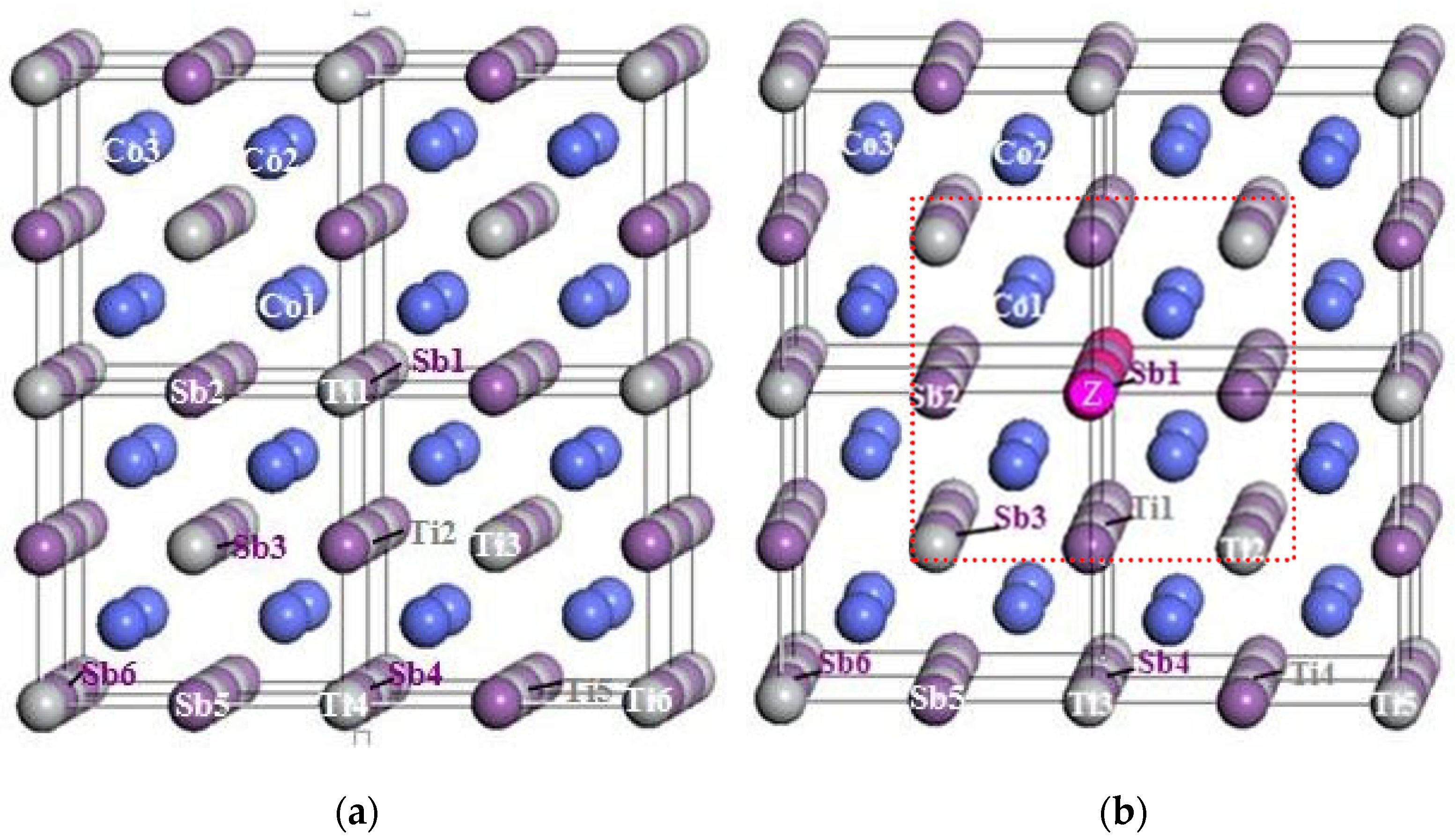
3.1. Crystal Structure

Figure 1a shows a schematic diagram of the unit cell structure of a semi-Heusler-structured CoTiSb alloy. As for CoTiSb, its semi-Heusler structure is observed as three (Co, Ti, Sb) face-centered cubic sublattices nested along a 1/4 diagonal in space. The atomic occupancy in a single cell is as follows: Co (0, 0, 0), Ti (0.25, 0.25, 0.25), and Sb (0.75, 0.75, 0.75). The Ti atom is replaced in a certain atomic chain of Z (Z = V, Cr, Mn, Fe, Co, Ni, Cu, Zn) along the crystallographic direction of the semi-Heusler-structured CoTiSb [001] to form a Z-Sb single-atom chain. The method of supercell was used to simulate and calculate the superstructure formed. In this study, the superstructure formed by replacing Ti with eight elements was assumed as shown in the superstructure in Figure 1b, and 2 × 2 × 2-unit cells were selected to form a basic superstructure unit. Replacing Ti atoms on the centerline Ti-Sb chain with Z atoms forms a superstructure centered on the Z-Sb atomic chain (referred to as Z-Sb supercell in this paper).

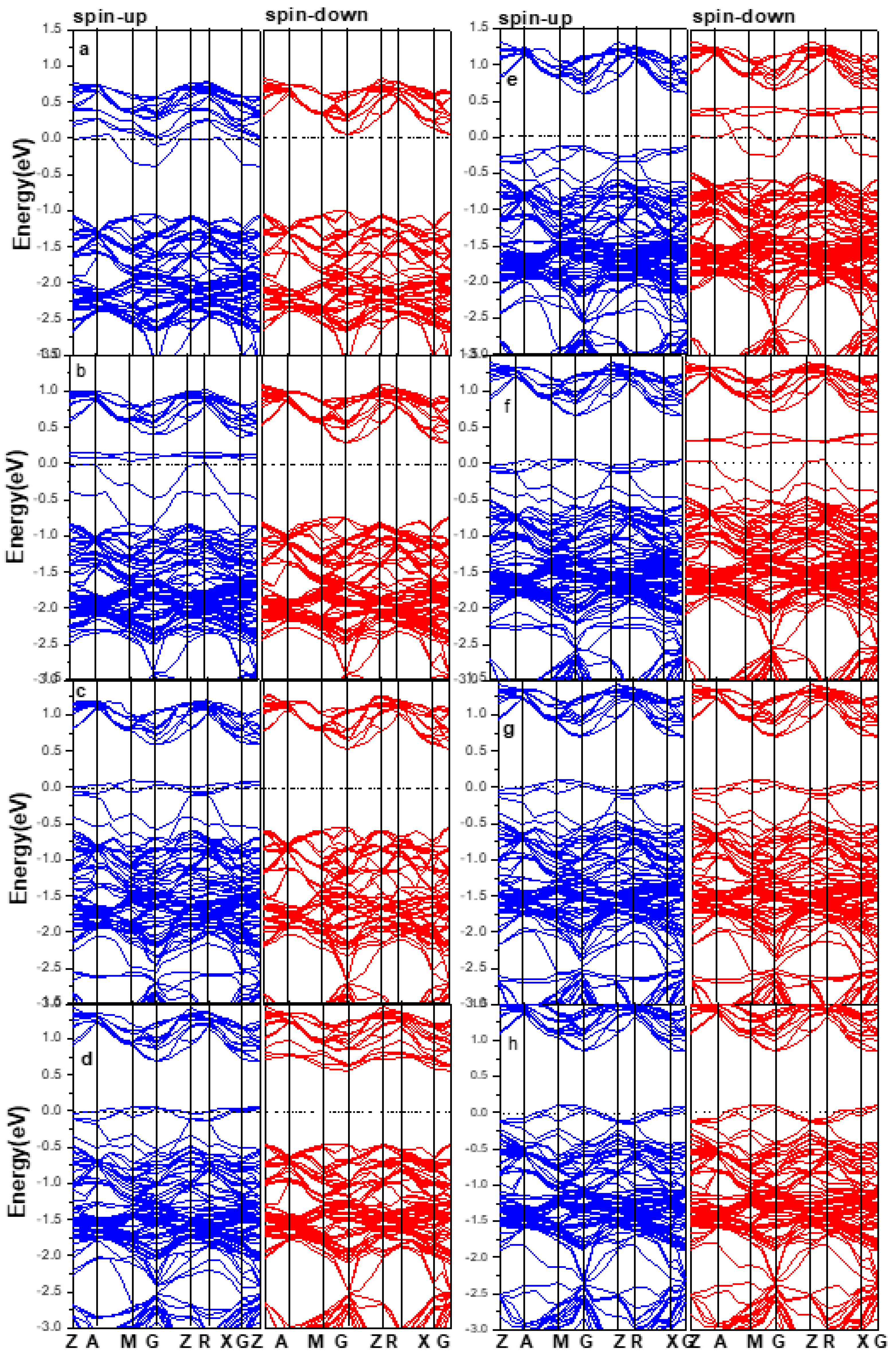
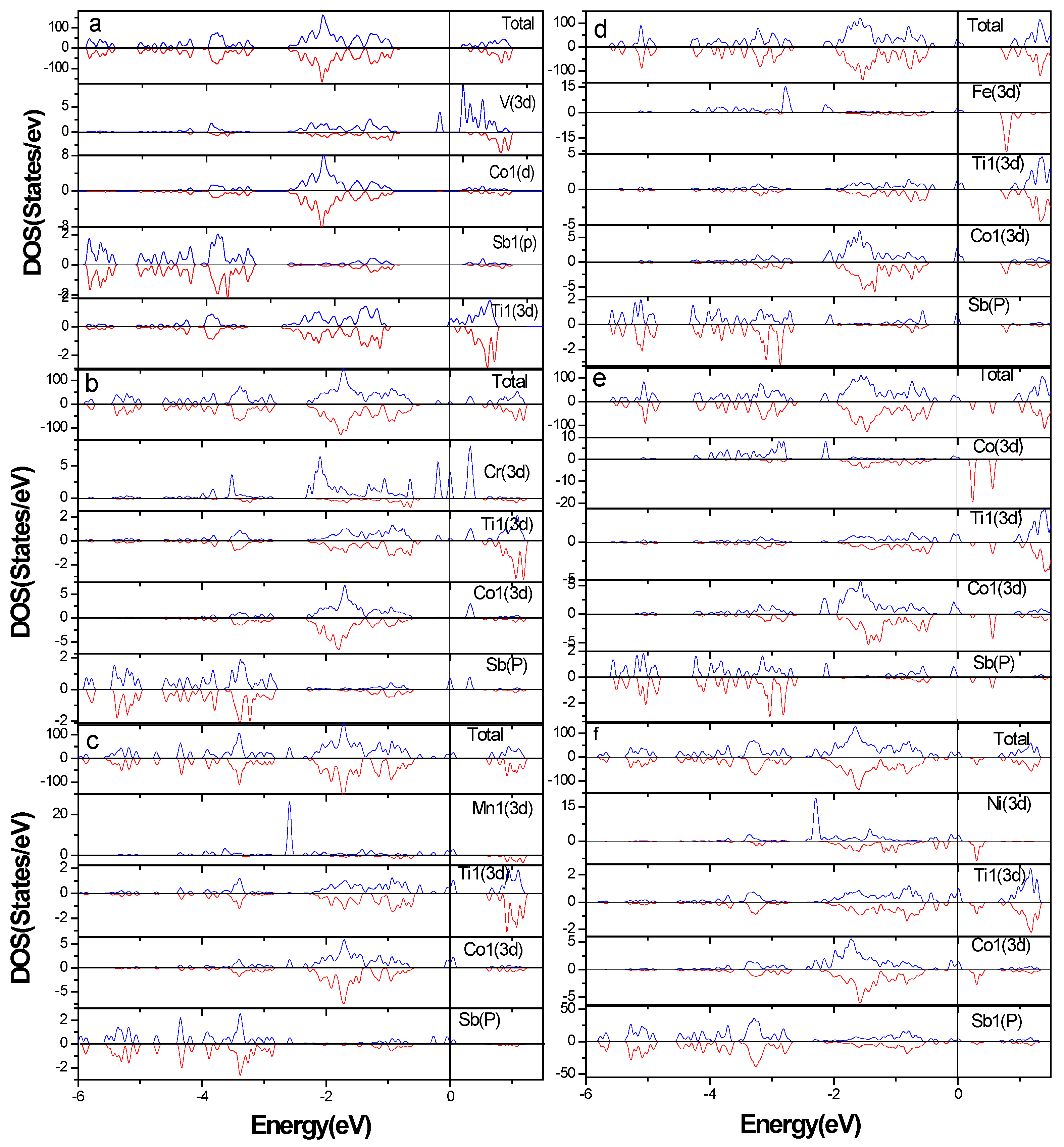
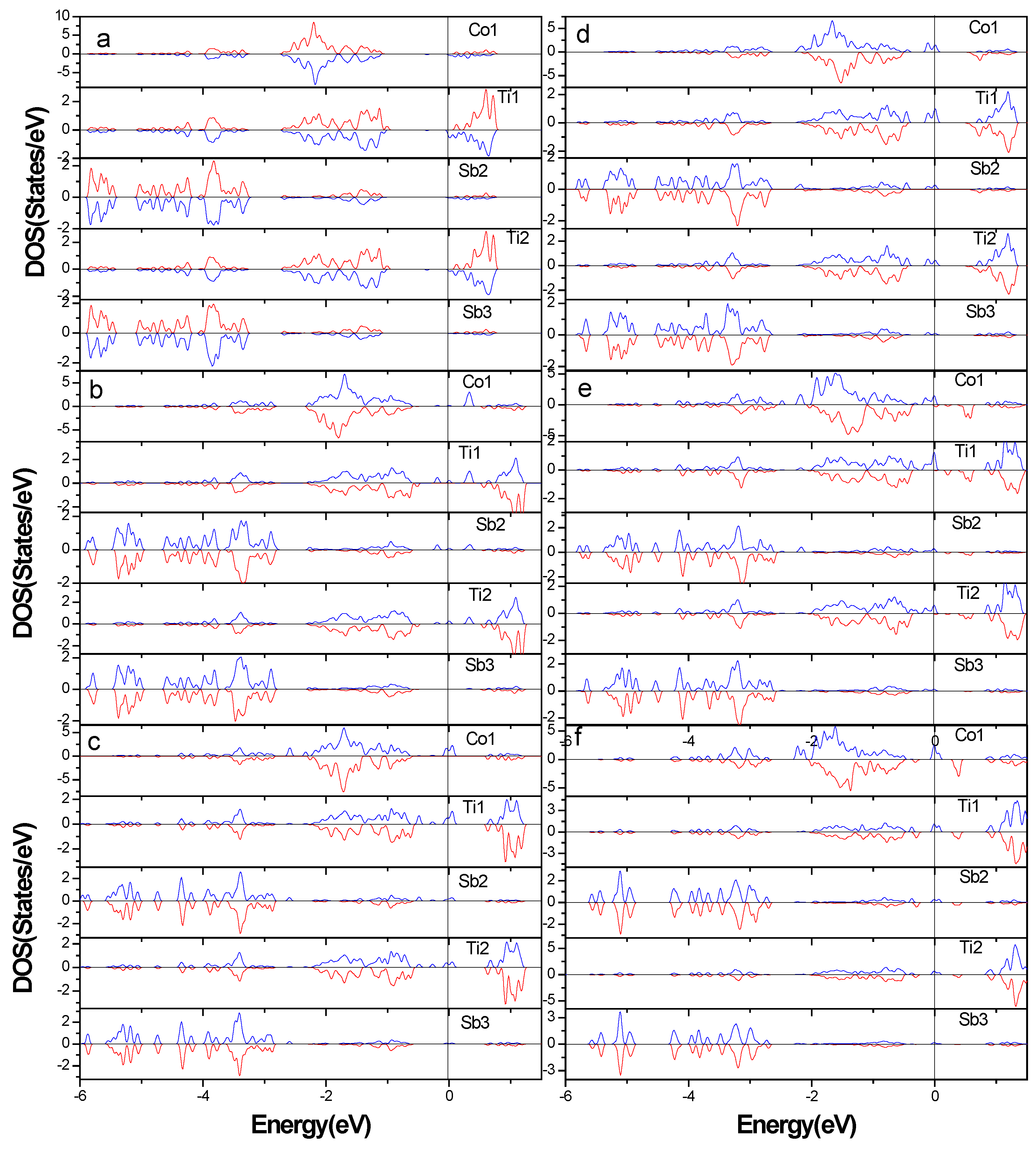
3.2. Electronic Structure of Supercells

Figure 2a–h show schematic diagrams of the band structures of eight types of supercells obtained through calculations. The band structures of Z-Sb (V, Cr, Mn, Fe, Co, Ni) supercells experience spin splitting, indicating that the doping of V, Mn, Fe, Cr, Ni, and Co elements results in ferromagnetic properties in the semiconductor CoTiSb material. Figure 2a (V-Sb supercell) shows that the bandgap of the CoTiSb matrix is approximately −1.0–0.4 eV. In the spin-up energy band, the impurity band induced by V doping is distributed in the forbidden band of the matrix, near −0.5–0.4 eV. The five energy bands distributed within this energy range have strong dispersion. With the partial density of states (PDOS), these five energy bands are mainly hybridized by the 3d orbital energy states of V and Ti elements and the 5p orbital energy state of Sb, with strong p-state characteristics (Figure 3). Impurity bands pass through the Fermi surface, forming a metallic intersection with the Fermi surface. That is, in the case of the V-Sb supercell, the conduction electrons on the Fermi surface have 100% spin polarization. In the spin-down band, the Fermi surface falls into an energy gap with a width of approximately 1.1 eV, exhibiting semiconductor properties. Therefore, V-Sb supercells exhibit typical semimetallic properties.
Figure 4 shows the PDOS spectra of each atom on the nearest, second, and third-nearest atomic chains of the V-Sb supercell center. The centerline V-Sb atomic chain affects the atoms on its nearest and second-nearest neighbor atomic chains, and has almost no effect on the atoms on the third-nearest neighbor atomic chain. The atoms on the atomic chains far from the V-Sb center in the matrix still maintain the semiconductor properties of the matrix. The dashed box in Figure 1b illustrates the range of influence of V-Sb atomic chains on the matrix atoms in the V-Sb supercell. This indicates that in the CoTiSb matrix, a V-Sb atomic chain centered lattice with a width of approximately a (where a is the lattice) has been formed constant conductive nanowires with 100% spin polarization.
In the spin-up band, the impurity bands induced by Cr doping are distributed around −0.75–0 eV and 0.2 eV in the matrix bandgap (Cr-Sb supercell) (Figure 2b). The two energy bands distributed in the range of −0.75–0 eV have strong dispersion. With the help of the PDOS of each atom (Figure 3b), these two energy bands are hybridized by the 3d orbital energy states of the Cr and Ti elements and the 5p orbital energy states of the Sb elements, with strong p-state characteristics. The three energy bands located near 0.2 eV are mainly formed by the hybridization of 3d orbital states of Cr, Co, and Ti, highlighting the high localization characteristics of 3d orbital states. In the spin-down band, the Fermi surface falls into an energy gap with a width of approximately 1.0 eV, exhibiting semiconductor properties. With the PDOS, Cr atoms have strong spin splitting, which makes the energy distribution of their spin-up band lower than that of their spin-down band (Figure 3b). The antibonding states formed by the hybridization of the 3d orbital states of Cr, Co, and Ti atoms exist in the spin-up direction, while there is no antibonding state formed by hybridization in the spin-down band. In the band structure and DOS spectrum, the Fermi surface slightly grazes the impurity-induced valence band top, while in the spin-down band, the Fermi surface falls into a direct bandgap. In other words, in the Cr-Sb supercell, the conduction electrons on the Fermi surface have a very low spin polarization rate of about 5%. Therefore, we conclude that in the spin down band its conductive characteristic belongs to hole conduction. Therefore, Cr-Sb supercells exhibit low-spin polarized-hole-conductivity properties. Figure 2c shows the band structure diagram of the Mn-Sb supercell formed by Mn replacing Ti. The band structure characteristics of the Mn-Sb supercell are similar to those of the Cr-Sb supercell. In contrast, in the spin-up band, the antibonding state formed by hybridization between the 3d electrons of Mn, Co, and Ti atoms exists around 0 eV. The antibonding state formed by hybridization between the 3d electrons of Cr, Co, and Ti atoms is around 0.2 eV. Moreover, in the Mn-Sb supercells, there is a metallic cross between the Fermi surface and the peak of the antibonding state in the spin-up band. In other words, electrons in the Mn-Sb supercells have 100% spin polarization at the Fermi surface, but the energy band located at the Fermi surface has strong localized properties and weak conductivity. In the spin-down band, the Fermi surface falls into an energy gap with a width of approximately 1.0 eV, exhibiting semiconductor properties. Therefore, the Mn-Sb supercells exhibit typical semimetallic properties. Correspondingly, the PDOS spectra of the atoms on the nearest, and second- and third-nearest atomic chains of the Mn-Sb central atomic chain are presented (Figure 4c). The Mn-Sb central atomic chain only affects the atoms on its nearest and second-nearest atomic chains, and has almost no effect on the atoms on the third-nearest atomic chain. In other words, the atoms further away from the Mn-Sb central atomic chain still maintain the semiconductor properties of the matrix. In this way, Mn replaces Ti to form a single-spin nanocolumn channel with the Mn-Sb atomic chain as the center and a width of approximately a (where a is the lattice constant) in the CoTiSb matrix.
In the band structure shown in Figure 2d (the Fe-Sb supercell), the band structure of the Fe-Sb supercell is similar to the band structure diagram of the Mn-Sb supercell. The Fe-Sb supercell is also a semimetallic material. The PDOS spectra of atoms on the Fe-Sb central atomic chain’s nearest, second, and third-nearest atomic chains are presented (Figure 4d). Similar to the situation in Mn-Sb supercells, Fe replaces Ti to form a single-spin nanocolumn channel centered on the Fe-Sb atomic chain and with a width of approximately a in the CoTiSb matrix.
Figure 2e shows the band structure diagram of the Co-Sb supercell. The bandgap of the CoTiSb matrix is approximately −0.5–0.75 eV. In the spin-down band, the distribution of impurity bands induced by Co doping in the matrix bandgap is −0.25–0.3 and 0.5 eV. The two energy bands are distributed in the energy range of −0.25–0.3 eV and have strong dispersion. The PDOS spectra of each atom in Figure 3e show that these two energy bands are composed of the hybridization of 3d orbital energy states of impurity Co and Ti atoms and 5p orbital energy states of Sb atoms, with strong p-state characteristics. The three energy bands located near 0.5 eV are mainly formed by the hybridization of 3d orbital energy states of Co and Ti atoms, highlighting the high localization characteristics of 3d orbital energy states. In the spin-up energy band, the distribution of the impurity band induced by Co doping in the matrix forbidden band is different from that in the spin-down energy band. The main difference is that the corresponding antibonding state in the spin-down band is around 0.5 eV, while in the spin-up band, it is around −0.2 eV.
The PDOS spectra of each atom (Figure 3e) show that the Co atom has strong spin splitting, resulting in a lower energy distribution of the antibonding state formed by hybridization between the 3d electrons of Co and Ti atoms in the spin-up band than in the spin-down band. Therefore, in the spin-down band structure and DOS spectra, there is a metallic crossing between the Fermi surface and impurities, indicating that the conduction electrons on the Fermi surface in Co-Sb supercells have 100% spin polarization. The semiconductor properties exhibited by the Co-Sb supercell occur due to the Fermi surface falling into an energy gap with a width of approximately 0.75 eV in the spin-up band. In the spin-down energy band, the impurity energy band induced by Ni atoms near the Fermi surface shows a strong dispersion of P electrons, indicating that the conductivity here is very strong. Therefore, Co-Sb supercells exhibit typical semimetallic properties. Correspondingly, Figure 4e shows the PDOS spectra of each atom’s nearest neighbor, and second- and third-nearest neighbors of the central atomic chain in the Co-Sb supercell. The Co-Sb atomic chain affects the atoms on its nearest and second-nearest neighbor atomic chains. In Figure 1b, a dashed box denotes the Co-Sb supercell. The range influences the central atomic chain on the matrix atoms. This indicates that a single-spin nanocolumn channel with a width of approximately a, centered on Co-Sb atomic chains, was formed in the CoTiSb matrix by replacing Ti with Co.
Figure 2f shows the band structure diagram of Ni-Sb supercells formed by Ni replacing Ti atoms. In the spin-up energy band, the Fermi surface passes through impurity bands, showing the characteristics of the metal. The Fermi surface was slightly rubbed on the top of the valence band, induced by impurity Ni atoms in the spin-up energy band. The electrons in the Ni-Sb supercell formed by Ni replacing Ti atoms have a high spin polarization rate of up to 95%. In the spin-down band, its conductivity is p-type conductivity (hole conductivity), and the band at the Fermi surface has strong localized properties in the spin-up band, indicating weak conductivity at this location. Therefore, Ni-Sb supercells exhibit highly spin-polarized-hole conductivity characteristics. Correspondingly, the PDOS spectra of atoms are observed on the nearest, and second- and third-nearest atomic chains of the central atomic chain in the Ni-Sb supercell (Figure 4f). The Ni-Sb monatomic chain is a single-spin nanoroad channel, as is the case with Co-Sb supercells.
The PDOS spectra of each atom on the nearest, and second- and third-nearest atomic chains of Z-Sb (Z = V, Cr, Mn, Fe, Co, Ni) supercell center atom chain are presented in Figure 4a–f. Compared with the band structure spectra of the Co-Sb and Ni-Sb supercells, the band structures of these two supercells are relatively similar, with five impurity bands distributed in the bandgap of the matrix. Moreover, antibonding states exhibit strong d-electron localization characteristics. The main difference between the two is the energy distribution of the antibonding state formed by hybridization between the 3d electrons of Co and Ti atoms. In the band structure diagrams of the Cu-Sb and Zn-Sb supercells (Figure 2g,h), impurity bands pass through the Fermi surface in both spin-up and spin-down bands, exhibiting metallic properties. This shows that the doping with Cu and Zn produces magnetism in the CoTiSb matrix, which changes the characteristics of the semiconductor into the characteristics of the metal.

3.3. Bandgap Width of Alloy

To observe the effect of dilute magnetic doping (doping elements are V, Cr, Mn, Fe, Co, Ni) on the CoTiSb alloy and the law of the change of the bandgap width of the CoTiSb alloy, the bandgap width values of these six supercells are listed in Table 1. The bandgap widths of V-Sb, Cr-Sb, Mn-Sb, and Fe-Sb supercells are the same at 1.0 eV. As the atomic number of the doping element increases, the bandgap width of the formed supercell gradually narrows, with the bandgap widths of the Co-Sb supercell and Ni-Sb supercell being 0.75 and 0.25 eV, respectively.

3.4. Total Magnetic Moment of Supercells

Table 2 lists the total magnetic moments of the Z-Sb (Z = V, Cr, Mn, Fe, Co, Ni, Cu, Zn) supercells. The total magnetic moment of supercells formed by doping elements with atomic numbers in the range of 23–28 is an integer. This is a typical characteristic of semimetallic materials. The total magnetic moment of the supercell formed by doping elements with atomic numbers between 23 and 27 increases with the increase in atomic numbers, which are 1.0, 2.0, 3.0, 4.0, and 5.0 µB, respectively. The Ni-Sb and Cr-Sb supercells have the same total magnetic moment, which is 2.0 µB. The total magnetic moment of the Cu-Sb and Zn-Sb supercells is not an integer, and their band structures and density-of-states graphs do not show semimetallic ferromagnetic properties.

4. Conclusions

The electronic structure and magnetic properties of CoTiSb doped by elements with atomic numbers in the range of 23–30 (V–Zn) are studied. The specific doping method is to replace the Ti atoms on the atomic chain along a certain crystallographic direction of the CoTiSb supercell. A series of Z-Sb (Z = V, Cr, Mn, Fe, Co, Ni, Cu, Zn) single-atom chains were designed using this method. The calculation results show that supercells containing Z-Sb (Z = V, Mn, Fe, Co) centerline atomic chains exhibit 100% spin polarization and exhibit semimetallic properties, making them excellent semimetallic magnetic materials. Ni-Sb supercells also exhibit a spin polarization rate of 95% and possess highly spin-polarized-hole conductivity characteristics.

Funding

This research received no external funding.

Institutional Review Board Statement

The study did not require ethical approval.

Informed Consent Statement

Not applicable.

Data Availability Statement

Data will be made available on request.

Conflicts of Interest

The author declares no conflict of interest.

References

  1. De Groot, R.A.; Mueller, F.M.; Van Engen, P.G.; Buschow, K.H.J. New class of materials: Half-metallic ferromagnets. Phys. Rev. Lett. 1983, 50, 2024–2027. [Google Scholar] [CrossRef]
  2. Sun, J.Z. Current-driven magnetic switching in manganite trilayer junctions. J. Magn. Magn. Mater. 1999, 202, 157–162. [Google Scholar] [CrossRef]
  3. Katine, J.A.; Albert, F.J.; Buhrman, R.A. Current-induced realignment of magnetic domains in nanostructured Cu/Co multilayer pillars. Appl. Phys. Lett. 2000, 76, 354–356. [Google Scholar] [CrossRef]
  4. Berger, L. Emission of spin waves by a magnetic multilayer traversed by a current. Phys. Rev. B 1996, 54, 9353–9358. [Google Scholar] [CrossRef] [PubMed]
  5. Bazaliy, Y.B.; Jones, B.A.; Zhang, S.C. Modification of the Landau-Lifshitz equation in the presence of a spin-polarized current in colossal-and giant-magnetoresistive materials. Phys. Rev. B. 1998, 57, R3213–R3216. [Google Scholar] [CrossRef]
  6. Weintal, X.; Myers, E.B.; Brouwer, P.W.; Ralph, D.C. Role of spin-dependent interface scattering in generating current-induced torques in magnetic multilayers. Phys. Rev. B. 2000, 62, 12317. [Google Scholar] [CrossRef]
  7. Wang, L.Y.; Dai, X.F.; Wang, X.T.; Li, Y.; Wu, Z.M.; Cui, Y.T.; Liu, G.D. Highly-spin-polarized interface in CoTiSb/Fe(Mn)/CoTiSb superlattice. Superlattices Microstruct. 2015, 86, 493–500. [Google Scholar] [CrossRef]
  8. Segall, M.D.; Lindan, P.J.D.; Probert, M.J.; Pickard, C.J.; Hasnip, P.J.; Clark, S.J.; Payne, M.C. First-principles simulation: Ideas, illustrations and the CASTEP code. J. Phys. Condens. Matter. 2002, 14, 2717–2744. [Google Scholar] [CrossRef]
  9. Perdew, J.P.; Burke, K.; Ernzerhof, M. Generalized Gradient Approximation Made Simple. Phys. Rev. Lett. 1996, 77, 3865–3868. [Google Scholar] [CrossRef] [PubMed]
  10. Galanakis, I.; Dederichs, P.H. Half-Metallic Heusler Alloys: Fundamentals and Applications; Springer: Berlin/Heidelberg, Germany, 2005; pp. 1–39. [Google Scholar]
  11. Prinz, G.A. Magnetoelectronics. Science 1998, 282, 1660–1663. [Google Scholar] [CrossRef] [PubMed]
  12. Planes, A.; Manosa, L.; Saxena, A. Magnetism and Structure in Functional Materials; Springer: Berlin/Heidelberg, Germany, 2005; pp. 58–112. [Google Scholar]
  13. Van Leuken, H.; De Groot, R.A. Half-metallic antiferromagnets. Phys. Rev. Lett. 1995, 74, 1171. [Google Scholar] [CrossRef] [PubMed]
  14. Pickett, W.E. Spin-density-functional-based search for half-metallic antiferromagnets. Phys. Rev. B 1998, 57, 10613. [Google Scholar] [CrossRef]
  15. Akai, H.; Ogura, M. Half-metallic diluted antiferromagnetic semiconductors. Phys. Rev. Lett. 2006, 97, 026401. [Google Scholar] [CrossRef] [PubMed]
  16. Galanakis, I.; Dederichs, P.H.; Papanikolaou, N.J.P.R.B. Origin and properties of the gap in the half-ferromagnetic Heusler alloys. Phys. Rev. B. 2002, 66, 134428. [Google Scholar] [CrossRef]
  17. Coey, J.M.D.; Venkatesan, M.; Bari, M.A. Half-Metallic Ferromagnets. In High Magnetic Fields; Berthier, C., Levy, L., Martinez, G., Eds.; Springer: Berlin/Heidelberg, Germany, 2002; Volume 595, pp. 377–396. [Google Scholar]
  18. Felser, C.; Fecher, G.H.; Balke, B. Spintronics: A challenge for materials science and solid-state chemistry. Angew. Chem. Int. Ed. 2007, 46, 668–699. [Google Scholar] [CrossRef] [PubMed]
  19. Kübler, J. First principle theory of metallic magnetism. Physica B+C 1984, 127, 257–263. [Google Scholar] [CrossRef]
  20. Pierre, J.; Skolozdra, R.V.; Gorelenko, Y.K.; Kouacou, M. From nonmagnetic semiconductor to itinerant ferromagnet in the TiNiSn-TiCoSn series. J. Magn. Magn. Mater. 1994, 134, 95–105. [Google Scholar] [CrossRef]
  21. Tobola, J.; Pierre, J.; Kaprzyk, S.; Skolozdra, R.V.; Kouacou, M.A. Crossover from semiconductor to magnetic metal in semi-Heusler phases as a function of valence electron concentration. J. Phys. Condens. Matter. 1998, 10, 1013. [Google Scholar] [CrossRef]
  22. Balke, B.; Fecher, G.H.; Gloskovskii, A.; Barth, J.; Kroth, K.; Felser, C.; Robert, R.; Weidenkaff, A. Doped semiconductors as half-metallic materials: Experiments and first-principles calculations of CoTi1−xMxSb (M = Sc, V, Cr, Mn, Fe). Phys. Rev. B 2008, 77, 045209. [Google Scholar] [CrossRef]
  23. Wang, L.Y.; Dai, X.F.; Wang, X.T.; Li, P.P.; Xia, Q.L.; Zhang, Y.; Cui, Y.T.; Liu, G.D. Single spin channels in Fe-doped CoTiSb semiconductor. Superlattices Microstruct. 2015, 83, 261–270. [Google Scholar] [CrossRef]
Figure 1. (a) Schematic diagram of the unit cell structure of a semi-Heusler-structured CoTiSb alloy; (b) schematic diagram of Z-Sb (Z = V, Cr, Mn, Fe, Co, Ni) supercell structure.
Engproc 98 00036 g001
Figure 2. Band structure diagrams of Z-Sb (Z = V, Cr, Mn, Fe, Co, Ni, Cu, Zn) supercells (ah).
Engproc 98 00036 g002
Figure 3. Total density of states and the density of states of each atom in Z-Sb (Z = V, Cr, Mn, Fe, Co, Ni) supercell (af).
Engproc 98 00036 g003
Figure 4. PDOS spectra of each atom on the nearest, second, and third nearest atomic chains of Z-Sb (Z = V, Cr, Mn, Fe, Co, Ni) supercell center atom chain (af).
Engproc 98 00036 g004
Table 1. Bandgap widths of Z-Sb (Z = V, Cr, Mn, Fe, Co, Ni, Cu, Zn) supercells. (The hyphen means ”non-existence”.).
SupercellBandgap/eV
V-Sb1.1
Cr-Sb1.0
Mn-Sb1.0
Fe-Sb1.0
Co-Sb0.75
Ni-Sb0.25
Cu-Sb-
Zn-Sb-
Table 2. Total magnetic moment of Z-Sb (Z = V, Cr, Mn, Fe, Co, Ni, Cu, Zn) supercells.
SupercellBandgap/eV
V-Sb1.0
Cr-Sb2.0
Mn-Sb3.0
Fe-Sb4.0
Co-Sb5.0
Ni-Sb2.0
Cu-Sb0.8 × 10−2
Zn-Sb1.0 × 10−1
Disclaimer/Publisher’s Note: The statements, opinions and data contained in all publications are solely those of the individual author(s) and contributor(s) and not of MDPI and/or the editor(s). MDPI and/or the editor(s) disclaim responsibility for any injury to people or property resulting from any ideas, methods, instructions or products referred to in the content.

