Proceeding Paper

Pseudo-Footless Domino Circuit-Based Design of Hamming (7, 4) Encoding/Decoding Complementary Metal-Oxide-Semiconductor Circuit †

Department of Electronics Engineering, National Chin-Yi University of Technology, Taichung 41170, Taiwan
*
Author to whom correspondence should be addressed.
Presented at the 2024 IEEE 6th Eurasia Conference on IoT, Communication and Engineering, Yunlin, Taiwan, 15–17 November 2024.
Eng. Proc. 2025, 92(1), 98; https://doi.org/10.3390/engproc2025092098
Published: 17 June 2025
(This article belongs to the Proceedings of 2024 IEEE 6th Eurasia Conference on IoT, Communication and Engineering)

Abstract

A Hamming (7, 4) code (seven output bits, four input data bits) encoding/decoding complementary metal-oxide-semiconductor (CMOS) circuit was studied. Based on previous static circuit designs, we modified it into a dynamic circuit. The circuit was implemented using the 0.18-μm 1P6M CMOS process of United Microelectronics Corp. The circuit functionality was simulated using HSPICE, and it was confirmed that the encoding/decoding circuits, self-error detection, and self-correction functions operate correctly. The circuit operated at a maximum frequency of 800 MHz.

1. Introduction

Hamming worked on elasticity theory at Bell Labs with the Bell Model V computer, which is an electromechanical relay-based machine [1]. The data or program of the calculating machines were represented as various small holes on the punched paper tape. However, the running programs of the calculating machine would be interrupted when the machine detected an error, and then the program had to be restarted after the error was removed. A complex program was sent to the machine to be calculated using the algorithm over one week but received an error message of peripheral malfunctions. For the next few years, Hamming studied error correction codes for code self-correction capability and published this as the Hamming code in 1950. The coded technique is still useful in error-correcting code (ECC) memory.
In Hamming code, four bits of data, D1, D2, D3, and D4, are encoded into seven bits by adding three parity bits, P1, P2, and P4, abbreviated as the Hamming (7, 4) representation. The formation of the whole data bits is organized as P1, P2, D1, P4, D2, D3, and D4 in order from the least significant bit (lsb) to the most significant bit (msb). After encoding, all the data bits are sent to the receiving site. At the receiving site, the logic value of three parity bits is checked to identify errors. If D1 is turned upside down from 1 to 0, and vice versa in the data transmission process, the receiving P1, P2, and P4 become logic 1, 1, 0, respectively. Similarly, D2 can be identified according to 1, 0, 1 of P1, P2, and P4. For the same reason, the data are considered correctly received when P1, P2, and P4 are at logic 0, 0, 0, respectively [1,2].
In modern communication, various technologies for data transmission have been proposed due to the advancement of science and technology. In the communication system, higher data throughput means faster responses and less data lag. The immediateness of data is important and sensitive in television programs or music programs online. However, the validity of data processing becomes challenging as bit duration time shortens.
As a result, the design of a high-speed circuit is essential to achieve a fast response. Due to the continuous scale-down in the chip fabrication process, the metal-oxide-semiconductor field-effect transistor (MOSFET) is manufactured on a 3 nm scale. Recently, the Apple A18 Pro, a 64-bit system on a chip (SoC), has been used in the iPhone 16 smartphone, as it was successfully manufactured by the TSMC. These advanced technologies enable the advantage of the MOSFET’s fast response, but the chip design suffers from capacitive coupling interference, inductive interference, leakage current, reduced voltage supply, and noise. Therefore, the design of a high-speed encoder/decoder circuit for error correction is useful to enhance overall system stability.
Based on the proposed circuit architecture of previous research, the Hamming (7, 4) circuit function is constructed to improve overall operating speed. In this study, the encoding and decoding circuits of Hamming (7, 4) were designed using CMOS technology and dynamic logic. The circuit functions were verified using the HSPICE circuit simulator, and a maximum operation frequency of 800 MHz was achieved in the simulation using CMOS 0.18-µm technology.

2. Basic Module

To improve the circuit operating speed, we used dynamic CMOS logic. Two basic CMOS digital circuits were reviewed: domino logic and pseudo-footless domino logic.

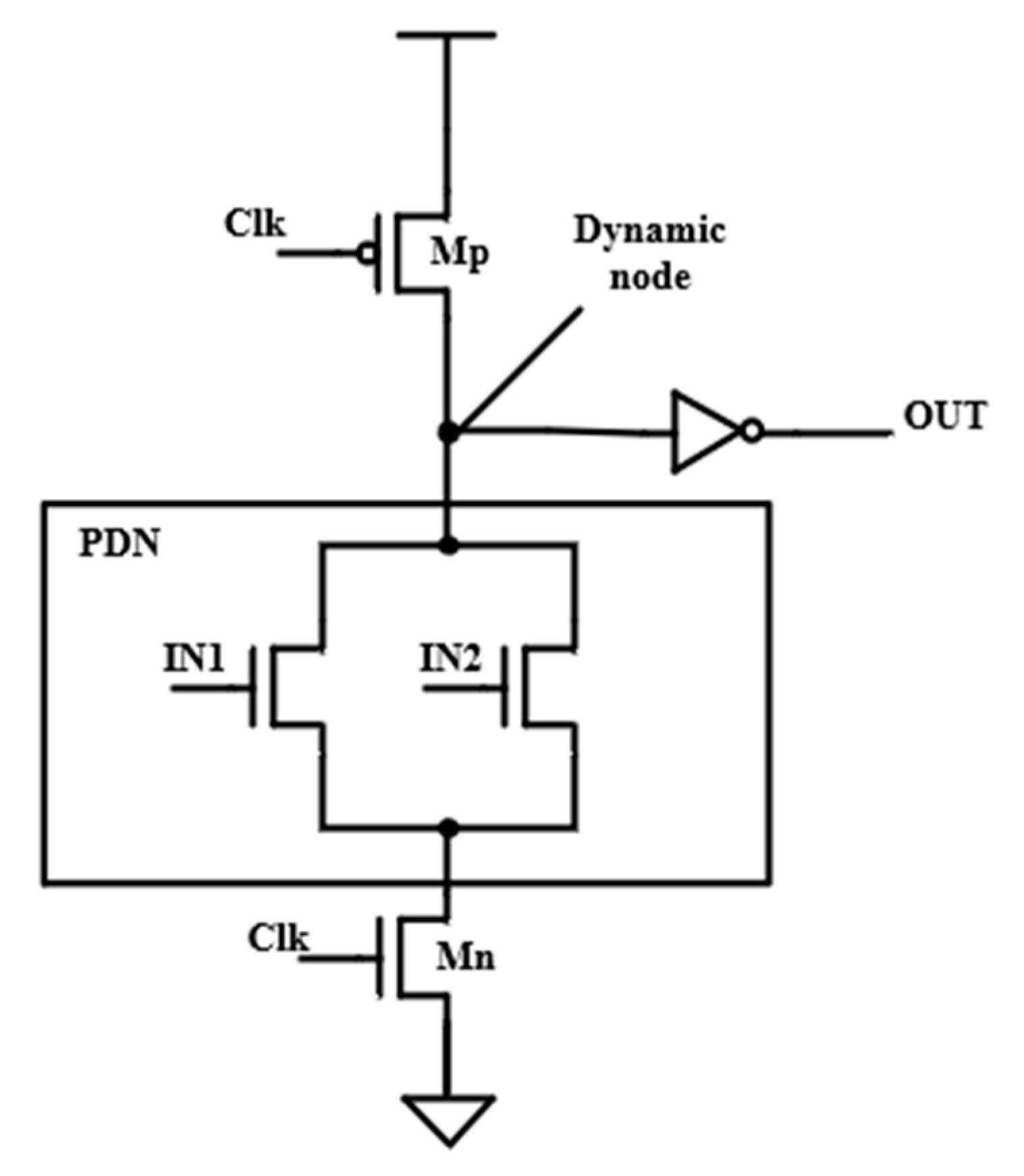
2.1. Domino Logic [3]

Figure 1 shows a domino logic circuit for the OR function. The circuit operates in two phases: a pre-charge phase and an evaluation phase. In the pre-charge phase, with Clk low (MP ON, MN OFF), the output node OUT is pre-charged low. In the evaluation phase, with Clk high (MP OFF, MN ON) the output node OUT responds to a proper logic level depending on the logic levels of inputs IN1 and IN2. In this case, the output node OUT responds to a logic high when either IN1 is high or IN2 is high, achieving the OR function. IN1 and IN2 signal-excited transistors are connected in parallel to perform the OR function. In the same derivation, a logic AND function is obtained if IN1 and IN2 signal-excited transistors are connected in series. In general, IN1/IN2 excited transistors determine the logic function, so the two transistors constitute the push-down network (PDN) (Figure 1).

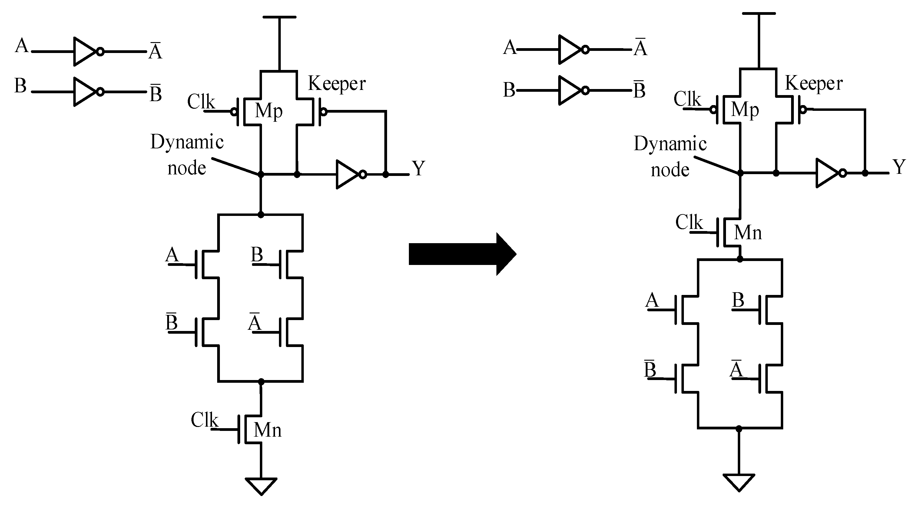
2.2. Pseudo-Footless (PF) Domino Logic [4,5]

The capacitance of the dynamic node (Figure 1) increases when the number of inputs increases. In addition, the synchronous problem of logic gates with more inputs is difficult. As a result, traditional domino logic suffers from the problem of charge sharing and larger capacitance when the number of inputs increases. The left part of Figure 2 shows a domino circuit for the XOR function [4,5]. The PMOS keeper transistor is designed to relieve the problem of the leakage current in a dynamic node. The keeper transistor tries to keep a low level enough when output Y is low. The right part of Figure 2 shows a PF domino circuit in the XOR function. The difference between the traditional domino and PF domino is the position of the Mn transistor (evaluation phase used). This ensures that the capacitance in the dynamic node is low enough despite the complexity of the PDN. As a result, the pre-charge and evaluated time are properly reduced, especially for a large-scale PDN. In addition, the total net charge in the dynamic node is lost in the pre-charge phase in the noise input of the PDN. Thus, the PF domino circuit relieves the problem of charge share.

3. Circuit Design [6,7]

The circuit architecture for implementing the PF domino Hamming code (7, 4) is shown in Figure 3. The original input data (D1–D4) must be encoded to generate an extra three parity bits (P1, P2, and P4). The combined bits P1, P2, D1, P4, D2, D3, and D4 are then sent to the receiving site via any communicated technology. In the receiving site, the checker and 3-to-8 decoder are used to check and identify which bit error occurs or does not occur. The checker generator is responsible for indicating the location of the error in binary form, and the data are then decoded with the 3-to-8 decoder. Finally, the correction block is used to correct the corresponding bit error.

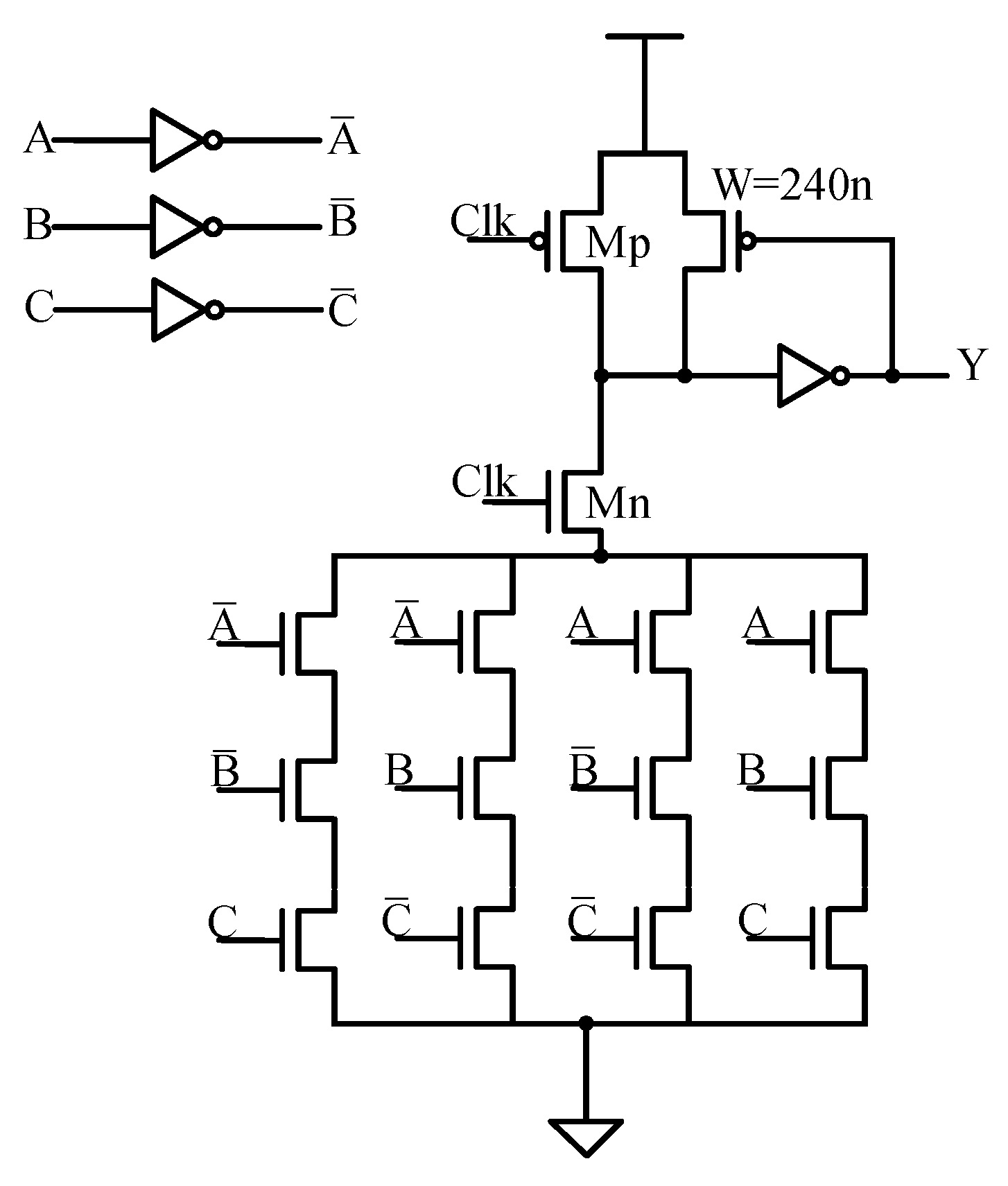
3.1. Three-Input XOR by PF Domino Circuit

Table 1 lists the truth table for the three-input XOR function where A, B, and C are inputs and Y is output. The Boolean equations are expressed as (1) and (2). Based on PF domino concept, a three-input XOR circuit is realized as shown in Figure 4.
Y = A B C
Y = A ¯ B ¯ C + A ¯ B C ¯ + A B ¯ C ¯ + ABC

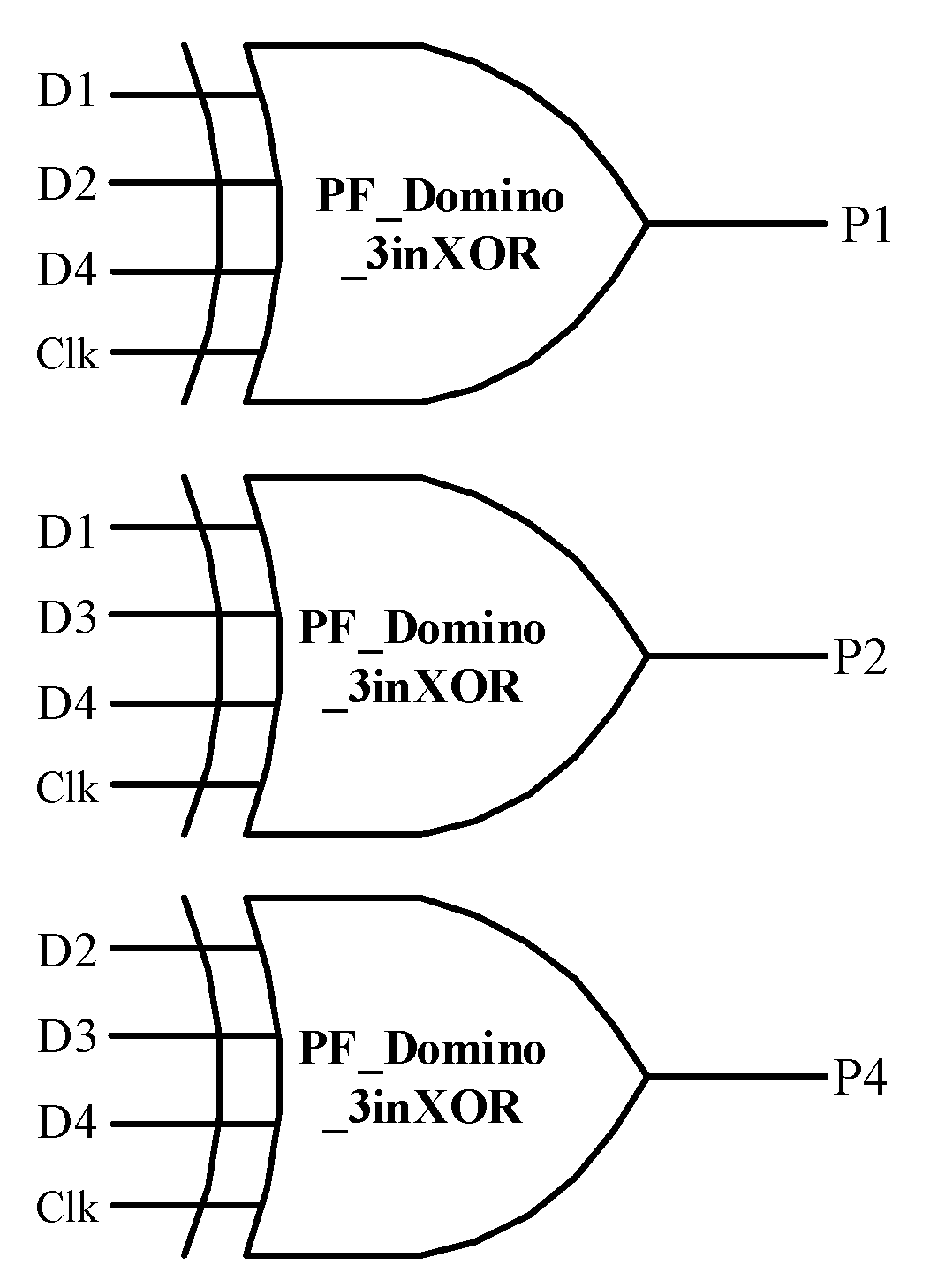
3.2. Encoder Circuit for Hamming Code

Equations (3)–(5) show the logical relationship between the check bits (P1, P2, and P4) and the original data bits (D1–D4). Figure 5 shows the encoder with a clock signal in the corresponding logic circuit. Figure 6 shows HSPICE simulation results. Parity bits P1, P2, and P4 respond correctly according to the logic value of D1–D4 inputs.
P1 = D1 ⊕ D2 ⊕ D4
P2 = D1 ⊕ D3 ⊕ D4
P4 = D2 ⊕ D3 ⊕ D4

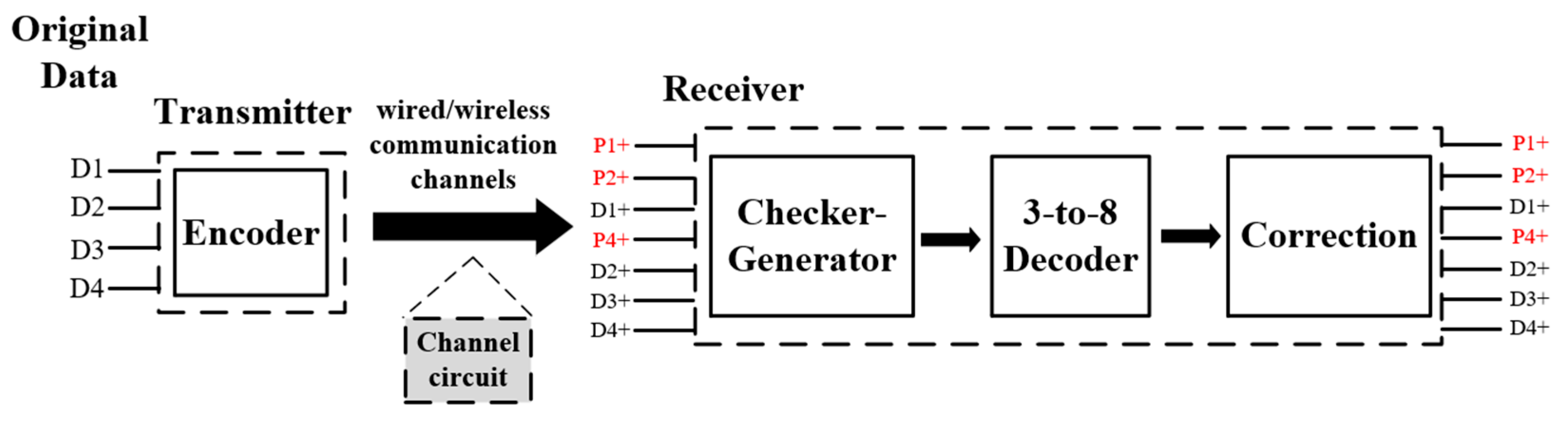
3.3. Channel Circuit

The multiplexer in Figure 7 is used to simulate errors occurring in wired/wireless communication channels. If the selected signal S is set to 1, the output of the multiplexer becomes the inverted signal of input data. If S is set to 0, outputs become the original input data.

3.4. Checker Generator Ccircuit

In the data transmission process, the checker generator in the receiving site is used to check the bit error occurrence. Based on the relationships in (3)–(5), the corresponding three checking bits C1, C2, and C3 are obtained as (6)–(8). The related circuits are shown in Figure 8. Due to the time delay in the logic circuit, the clock signals in the first and subsequent stages must be different in phase (Figure 8).
C1 = P1 ⊕ D1 ⊕ D2 ⊕ D4
C2 = P2 ⊕ D1 ⊕ D3 ⊕ D4
C3 = P3 ⊕ D2 ⊕ D3 ⊕ D4

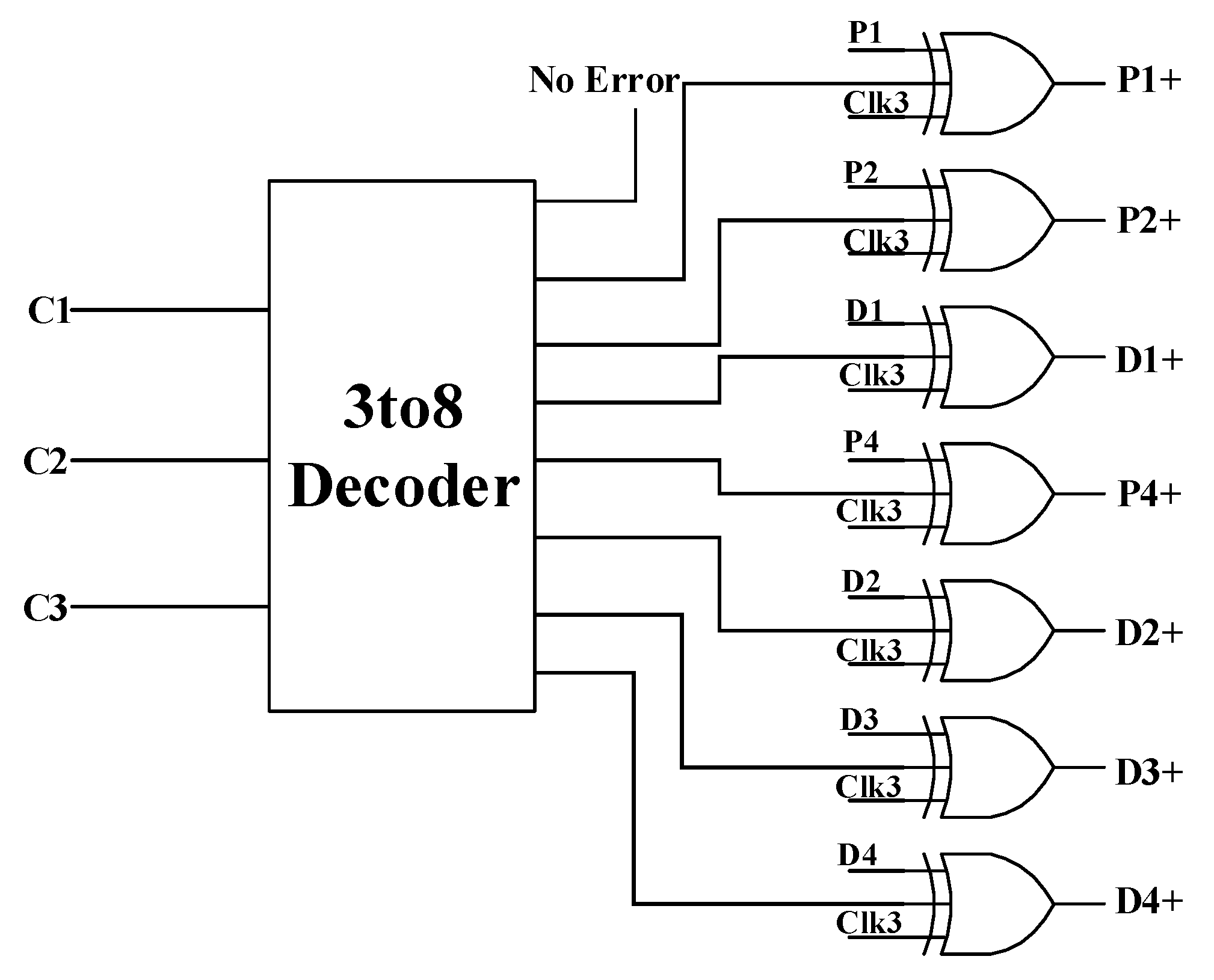
3.5. The 3-to-8 Decoder Circuit

Figure 9 shows the 3-to-8 decoder circuit. The check bit generator identifies the position of the erroneous data bit in binary form by using three check bits. After decoding these check bits, output 1 of the decoder corresponds to the position of the error bit.

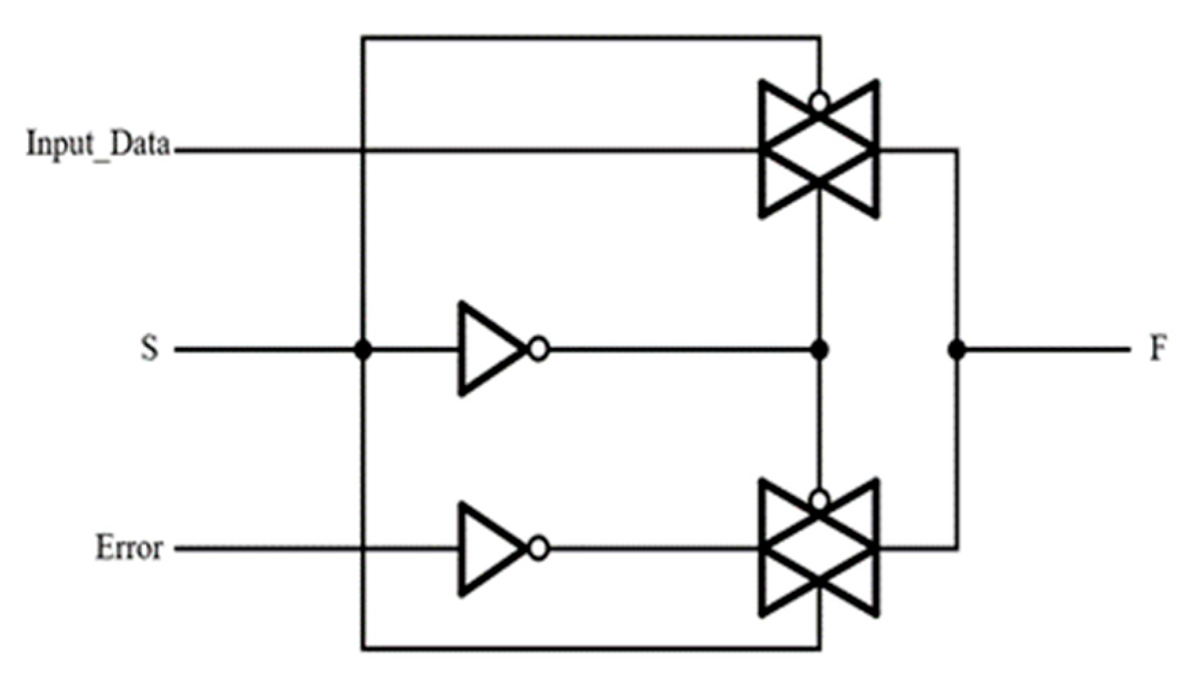
3.6. Correction Circuit

Figure 10 shows the 3-to-8 decoder and correction circuit. The correction circuit is composed of seven three-input XORs. In the error correction circuit, outputs P1+, P2+, D1+, …, D4+ in Figure 10 represent error-free data.

3.7. Clock Delay Circuit [8]

Figure 11 shows the error output of a two-input PF XOR circuit under one input has not settled to a stable logic 1 while clock signal Clk is already in the evaluation phase. That is, the clock signal is out of sync with the input-ready signal. The red box in Figure 11 indicates the time difference and discharge of the dynamic node. The blue box in Figure 11 shows the XOR error output 1 with two inputs in logic 1. Therefore, several clocks are generated in the circuit. The clock delay circuit in Figure 12 allows the phase of clock Clk1 leads Clk2, and also Clk2 leads Clk3 to compensate for the time delay in data processing.

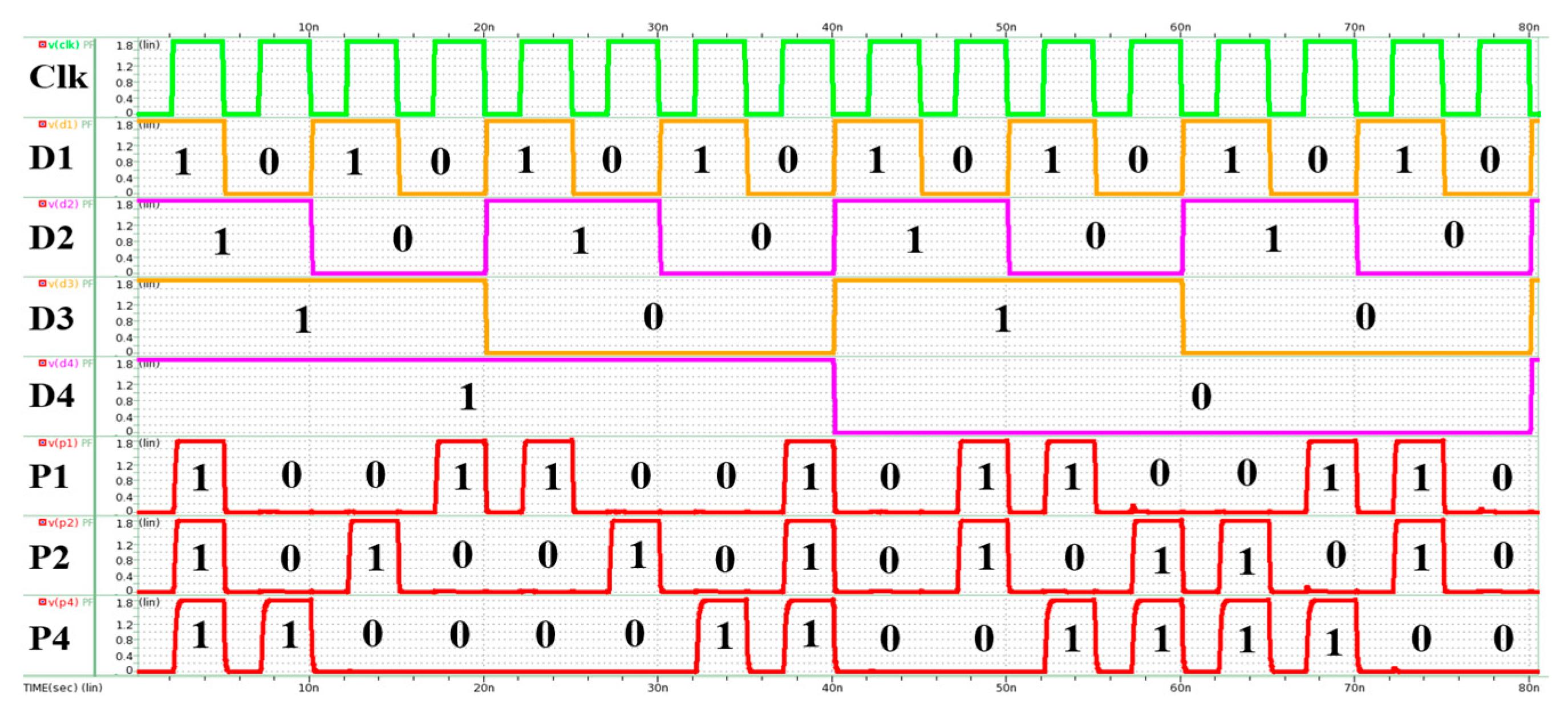
4. Circuit Simulation and Analysis

The function of the circuit is verified using HSPICE simulation. The simulation results are shown for the received D4 error and P4 error. D1-D4 are original input data bits while P1, P2, and P4 are parity bits.

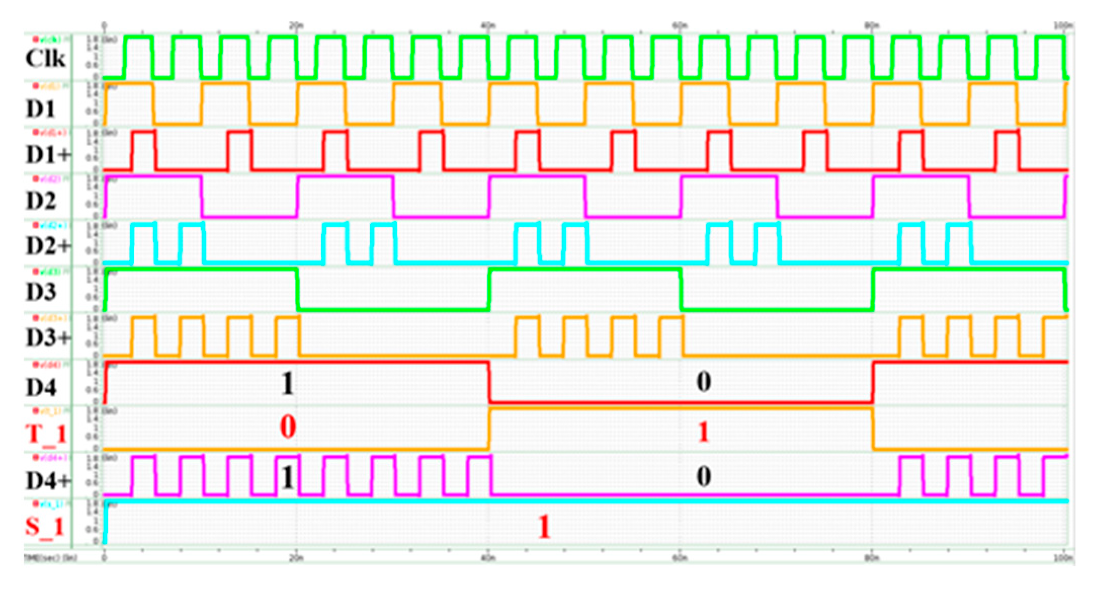
4.1. Simulation of D4 Error

Figure 13 shows the simulation results. First, the received bit D4 output is set to the wrong status of T_1 into the circuit; that is, error signal T_1 is the inversion of the right D4 bit. After circuit operation, the right D4+ output is corrected as D4 with high Clk due to dynamic logic. Based on the results, the error signal is corrected successfully.

4.2. Simulation of P4 Error

Another test example for the P4 error is shown in Figure 14. The correct original P4 bit is replaced by an error signal T_2. After circuit operation, P4+ exactly matches P4 with high Clk. The bit error is automatically corrected by the design of Hamming (7, 4) code.
Table 2 lists the circuit characteristics. The first circuit type is the Hamming encoding/decoding circuit with static PTL. The second circuit type is a general domino logic N-P series. The third circuit type is the PF domino architecture. The proposed PF domino circuit is evaluated for operating speed, and a maximum frequency of 800 MHz in PF domino is achieved. However, the transistor count and power consumption are larger than that of the other circuit types.

5. Conclusions

We designed the Hamming (7, 4) code of a four-bit encoding/decoding CMOS circuit using the pseudo-footless (PF) domino technique. The functions of encoding, bit error identification, and automatic correction were verified with HSPICE simulation in the UMC 0.18-μm process. Under 1.8 V and a frequency of 200 MHz, the PTL circuit had better performance in terms of transistor count and power consumption. However, the PF domino type showed a time delay and higher maximum frequency compared with the N-P domino and PTL types.

Author Contributions

Conceptualization, K.-M.H. and Y.-C.H.; methodology, K.-M.H.; software, K.-M.H.; validation, K.-M.H.; formal analysis, K.-M.H. and Y.-C.H.; investigation, K.-M.H.; resources, Y.-C.H. and J.-C.S.; data curation, K.-M.H.; writing—original draft preparation, K.-M.H.; writing—review and editing, J.-C.S. and Y.-C.H.; visualization, K.-M.H.; supervision, J.-C.S. and Y.-C.H. All authors have read and agreed to the published version of the manuscript.

Funding

This research received no external funding.

Institutional Review Board Statement

Not applicable.

Informed Consent Statement

Not applicable.

Data Availability Statement

No new data were created or analyzed in this study. Data sharing is not applicable to this article.

Acknowledgments

We would like to express our gratitude to the United Microelectronics Corporation (UMC) and the Taiwan Semiconductor Research Institute (TSRI) for providing the Version 1.0 of the EDA software that allowed us to perform IC layout and simulations at our laboratory.

Conflicts of Interest

The authors declare no conflict of interest.

References

  1. Wikipedia. Hamming Code. Available online: https://en.wikipedia.org/wiki/Hamming_code (accessed on 18 October 2023).
  2. Hamming, R.W. Error detecting and error correcting codes. Bell Syst. Tech. J. 1950, 29, 147–160. [Google Scholar] [CrossRef]
  3. Wikipedia. Domino Logic. Available online: https://en.wikipedia.org/wiki/Domino_logic (accessed on 25 October 2023).
  4. Chiu, W.-H.; Yeh, T.-T.; Lin, H.-R. A Conditional Isolator Technique for Wide Pseudo-Footless Domino Logic Circuits. J. Sci. Eng. Technol. 2008, 4, 13. [Google Scholar]
  5. Wang, J.-S.; Shieh, S.-J.; Yeh, C.-W.; Yeh, Y.-H. Pseudo-footless CMOS domino logic circuits for high-performance VLSI designs. In Proceedings of the 2004 IEEE International Symposium on Circuits and Systems (ISCAS), Vancouver, BC, Canada, 23–26 May 2004; pp. 402–403. [Google Scholar]
  6. Mokara, D.; Naidu, S.; Gupta, A.K. Designand implementation of Hamming Code using VHDL & DSCH. Int. J. Latest Eng. Res. Appl. (IJLERA) 2017, 2, 33–40. [Google Scholar]
  7. Lin, D.-L. Implementation of 8-Bit Hamming Encoder/Decoder Circuit. Master’s Thesis, Electronic Engineering from the National Chin-Yi University of Technology, Taichung, Taiwan, 2020. [Google Scholar]
  8. Yee, G.; Sechen, C. Clock-delayed domino for dynamic circuit design. IEEE Trans. Very Large Scale Integr. (VLSI) Syst. 2000, 8, 425–430. [Google Scholar]
Figure 1. Basic domino logic circuit for OR function.
Engproc 92 00098 g001
Figure 2. Basic domino XOR (left) and pseudo-footless (PF) domino XOR (right) circuits.
Engproc 92 00098 g002
Figure 3. Circuit architecture of Hamming (7, 4) code.
Engproc 92 00098 g003
Figure 4. Three-input XOR by PF domino.
Engproc 92 00098 g004
Figure 5. Design of encoder circuit.
Engproc 92 00098 g005
Figure 6. Simulation results of encoder.
Engproc 92 00098 g006
Figure 7. Channel circuit.
Engproc 92 00098 g007
Figure 8. Checker generator circuit.
Engproc 92 00098 g008
Figure 9. Decoder circuit.
Engproc 92 00098 g009
Figure 10. Correction circuit.
Engproc 92 00098 g010
Figure 11. XOR simulation results of clocks without delay.
Engproc 92 00098 g011
Figure 12. Clock delay circuit.
Engproc 92 00098 g012
Figure 13. Simulation results with D4 error.
Engproc 92 00098 g013
Figure 14. Simulation results with P4 error.
Engproc 92 00098 g014
Table 1. True table of three-input XOR.
ABCY
0000
0011
0101
0110
1001
1010
1100
1111
Table 2. Characteristic comparison.
PTL [3]N-P DominoPF Domino
Transistors count232357 (+54%)388 (+67%)
Power consumption @ 100 MHz210 μW347 μW (+65%)387 μW (+84%)
Delay @ 100 MHz1.21 ns377 ps (−69%)204 ps (−83%)
Maximum frequency250 MHz660 MHz (+164%)800 MHz (+220%)
Power consumption at max. frequency442.8 μW1.22 mW1.48 mW
Minimum frequency50 MHz50 MHz50 MHz
Power consumption at min. frequency167.6 μW152.6 μW177 μW
Disclaimer/Publisher’s Note: The statements, opinions and data contained in all publications are solely those of the individual author(s) and contributor(s) and not of MDPI and/or the editor(s). MDPI and/or the editor(s) disclaim responsibility for any injury to people or property resulting from any ideas, methods, instructions or products referred to in the content.

