Abstract
The integrated circuit (IC) industry has rapidly developed, with chip hardware security assuming a critical role in IC design. The physical unclonable function (PUF) exploits semiconductor process variation differences to generate unique responses randomly. Due to its non-replicability, PUF has emerged as one of the most commonly employed methods in hardware security. We propose PUF implementation employing an automatic scan selector to toggle between eight sets of multiplexers. With an 8-bit selector, 256 state inputs are automatically generated, and the PUF architecture enables a 256-bit unique identification code for the chip. Finally, the generated identification code is outputted either serially or in parallel and implemented on a field-programmable gate array platform.
1. Introduction
Hardware security heavily relies on identity recognition to mitigate its vulnerability to various attacks. In the authentication protocol, a large amount of computing resources needs to be consumed for encryption protection to ensure the security of data. With the rapid increase in the number of Internet of Things (IoT) devices, traditional encryption technology and authentication methods become increasingly inappropriate due to the high resource demands they impose [1]. Physical unclonable function (PUF) is used as a low-cost authentication and encryption solution in IoT, It leverages small process variations in hardware components by unintended differences that occur naturally during the manufacturing process to generate security keys that are difficult to copy. PUF provides keys that are reliable, unpredictable, and unique under limited computing power and power consumption [2].
PUF circuits are a hardware security technology that generates unique identification codes using physically non-replicable characteristics [3], with no sensitive information stored on the chip [4]. The basic principle of PUF circuits is to exploit the small random differences in the manufacturing process. These small physical differences affect the specific parameters of the circuit. These differences are unique to each wafer. Even under the same manufacturing conditions, two identically designed wafers have different characteristics because of these differences. Because the identification code generated by PUF is based on the intrinsic characteristics of the hardware rather than the software algorithm, it is difficult to attack through reverse engineering or cloning attacks.
The commonly used PUFs in different systems are as follows.
1.1. Static Random Access Memory (SRAM) PUF
The SRAM PUF exploits the power-on initialization state of SRAM cells. The initialization of each SRAM cell to 0 or 1 depends on minor manufacturing differences, resulting in a unique bit pattern [5]. The features of this architecture include a stable response, as the power-on state of SRAM cells tends to be consistent under the same conditions. Additionally, it offers compatibility with existing SRAM technology, allowing it to be easily integrated into standard memory components without requiring significant modifications.
1.2. Arbiter PUF
An Arbiter PUF generates a unique response by transmitting two signals along separate paths within the circuit and determining which signal arrives first at the destination. The differences in signal arrival times, or delays, are caused by subtle variations in the manufacturing processes of the device [2]. The features of using this architecture include simple structure and high response diversity.
1.3. Ring Oscillator PUF
This uses multiple ring oscillators and compares the frequency of each oscillator to produce a unique response. The frequency differences between the oscillators arise from small variations in the manufacturing process [6]. The features of using this architecture include a high response bit density, as each pair of oscillators produces a bit of the response, allowing for the generation of a large number of bits from relatively few oscillators [7].
1.4. Butterfly PUF
This uses cross-coupled latches, where the initialization state of these latches generates a unique bit pattern. When the latches are powered on, they resolve to either a 0 or 1 state based on minute, unpredictable differences in the circuit elements caused by manufacturing variations. The features of this architecture include similarities to SRAM PUF and enable more controlled initialization than SRAM PUF.
1.5. Glitch PUF
This exploits power supply spikes and glitches (momentary voltage fluctuations) and produces unique bit patterns based on the system’s response to them. A notable feature of this architecture is its high resistance to attacks, as the unpredictable and transient nature of the glitches makes it difficult for attackers to replicate or model the system’s response.
We used an Arbiter PUF as there are many uncertain factors in path delay and an Arbiter PUF has the advantages of low power consumption, high speed, and small physical size. Therefore, it is effective and controllable for hardware security.
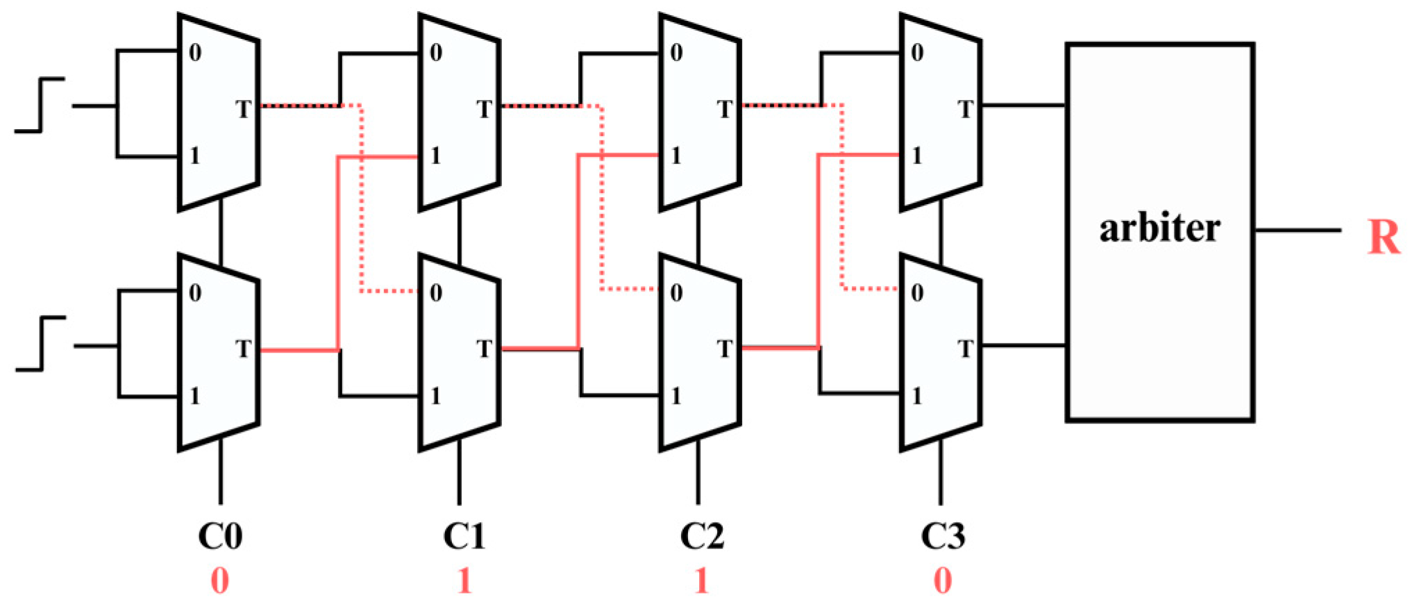
2. Arbiter PUF Architecture
An Arbiter PUF is a strong PUF based on path delay, making it a robust and versatile hardware security primitive due to its large number of challenge-response pairs (CRPs), as shown in Figure 1 [2]. The structure of an Arbiter PUF consists of multiple 2:1 multiplexers connected in parallel, forming groups that are sequentially connected through direct connections and cross-connections [8]. Each multiplexer group is responsible for routing the input signals based on a specific challenge. A challenge is a binary sequence that determines the path taken by the signals through the multiplexers. For instance, in the first group of multiplexers that share the same signal, the challenge bit decides whether the signal takes a straight path (denoted by 1) or a cross path (denoted by 0). When there are N sets of multiplexers, exactly N bits are required, each bit controlling the path through one set of multiplexers. These paths have inherent delays due to minor, unpredictable variations in the manufacturing process. These variations result in slight differences in the time it takes for the signals to travel through each path. The Arbiter, typically implemented as a latch, captures the timing difference between the two signals as they arrive. Depending on which signal arrives first, the arbiter will output either a 0 or a 1.
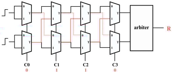
Figure 1.
PUF architecture diagram.
This process results in a unique response for each challenge, determined by the specific delays along the chosen paths. The simplicity of the Arbiter PUF’s architecture, combined with its ability to generate a vast number of unique responses, makes it highly efficient and effective for security applications. The high response diversity of this architecture is critical for creating secure, unclonable identifiers for devices, contributing to its widespread use in cryptographic systems.
3. Automatic Counter PUF
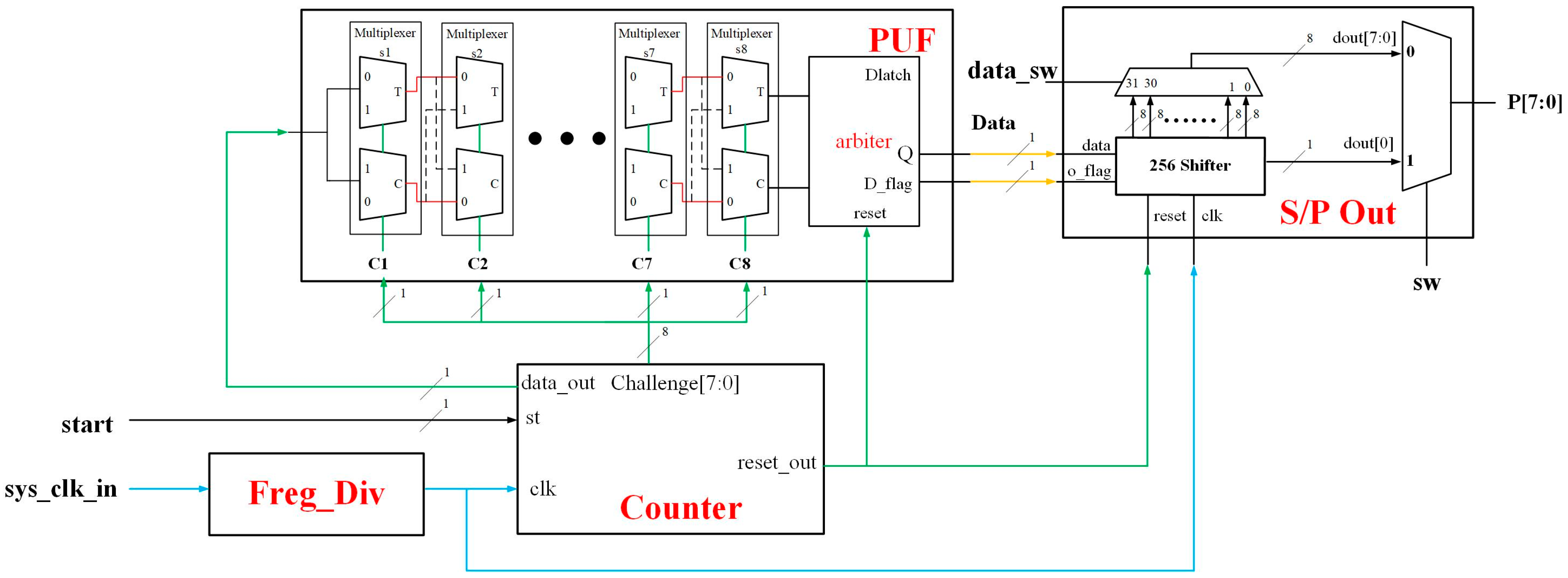
As shown in Figure 2, the PUF in this study is composed of the following modules.
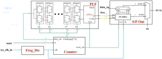
Figure 2.
Automatic PUF architecture.
3.1. Freq_Div Circuit
Using the frequency divider allows the user to determine the input frequency and clearly observe various parameter changes and output signals on the verification board.
3.2. PUF and Counter Circuits
Data_out is used as the input of PUF and the challenge generated by Counter is used as the selection line. reset_out inputs the reset signal to D-Latch to clear the register data. As shown in the PUF timing diagram in Figure 3, every 100 ms challenge is input. The reset and input signals are applied sequentially for each challenge, with the reset signal being asserted first, followed by the input signal after a brief delay, and the result will be an irregularly changing wave pattern of 0 and 1.
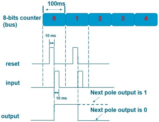
Figure 3.
PUF timing diagram.
3.3. S/P out Circuit
This module stores the PUF output value in a 256-bit register and uses a multiplexer to select the output as 1-bit serial output or 8-bit parallel output. When selecting serial output, a circular shift method will be used. After the serial output is completed, a parallel output can be performed.
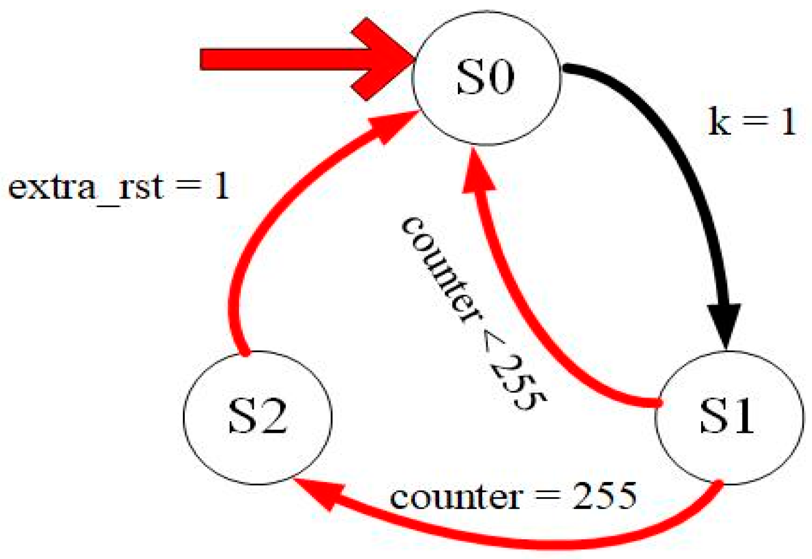
3.4. State Machine Circuit
As shown in Figure 4, a state machine can be used to control the executed program. It initially enters S0. Every time a piece of data is received, the counter increases by 1 and sends a k = 1 signal. S1 sends reset and input signals and determines whether the counter value is equal to 255. If not, the value becomes S0, and counting continues. If yes, S2 is input, data transmission completes, and counting stops. The value returns to S0 and the next take starts.

Figure 4.
Counter block state diagram.
In Algorithm 1, the output is selected as serial or parallel. When a parallel output is selected, because 8 bits are output at a time, a counter is used combined with a state machine to output 32 pieces of data.
| Algorithm1: Serial and parallel output algorithms |
| Input: 1. data[256] 2. count = 0 3. if(sw = 0) then 4. for k = 0 to 31 do 5. for n = 0 to 7 do 6. Parallel_out[k][n] = data[count] 7. count++ 8. end for 9. end for 10. Output Parallel_out 11. else if (sw = 1)then 12. *Serial_out = *data 13. Output Serial_out 14. end if |
4. Results and Discussion
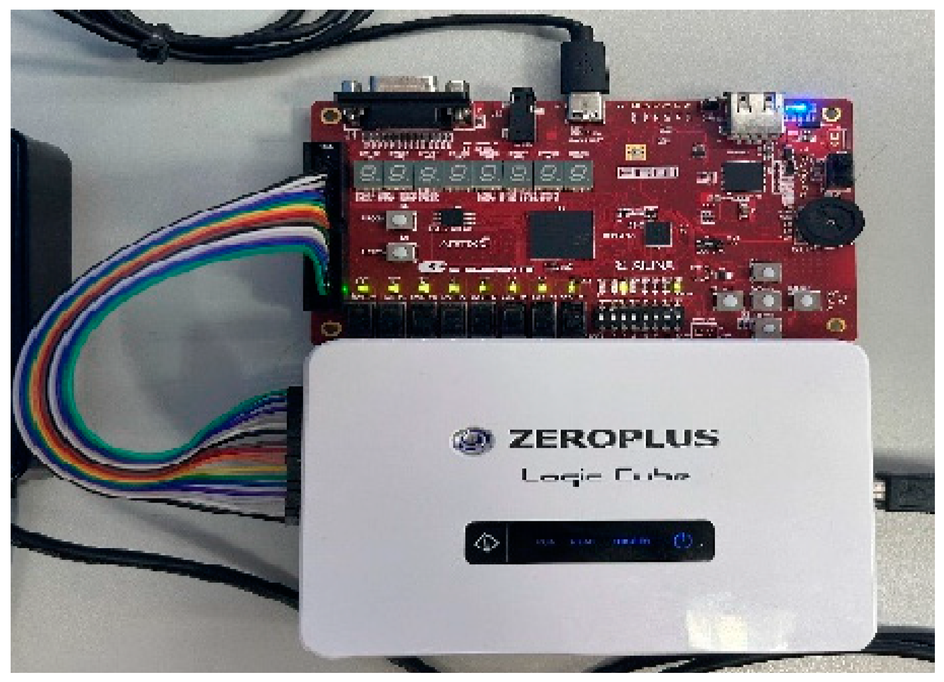
Figure 5 shows the PUF implementation diagram. We used the Xilinx Artix-7 FPGA XC7A35T development board (EGO) as the verification platform and output the counter through LED[7:0]. When the counter jumps, the 1-bit output is stored in the temporary register. When the 256-bit value is stored, LED lights up to indicate the completion of the transmission. The DIP switch is used as an analog state machine to select the output serial and parallel types. A logic analyzer is used to capture the output information for observation.
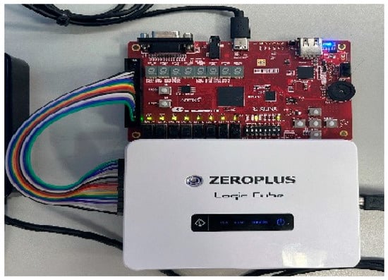
Figure 5.
PUF implementation diagram.
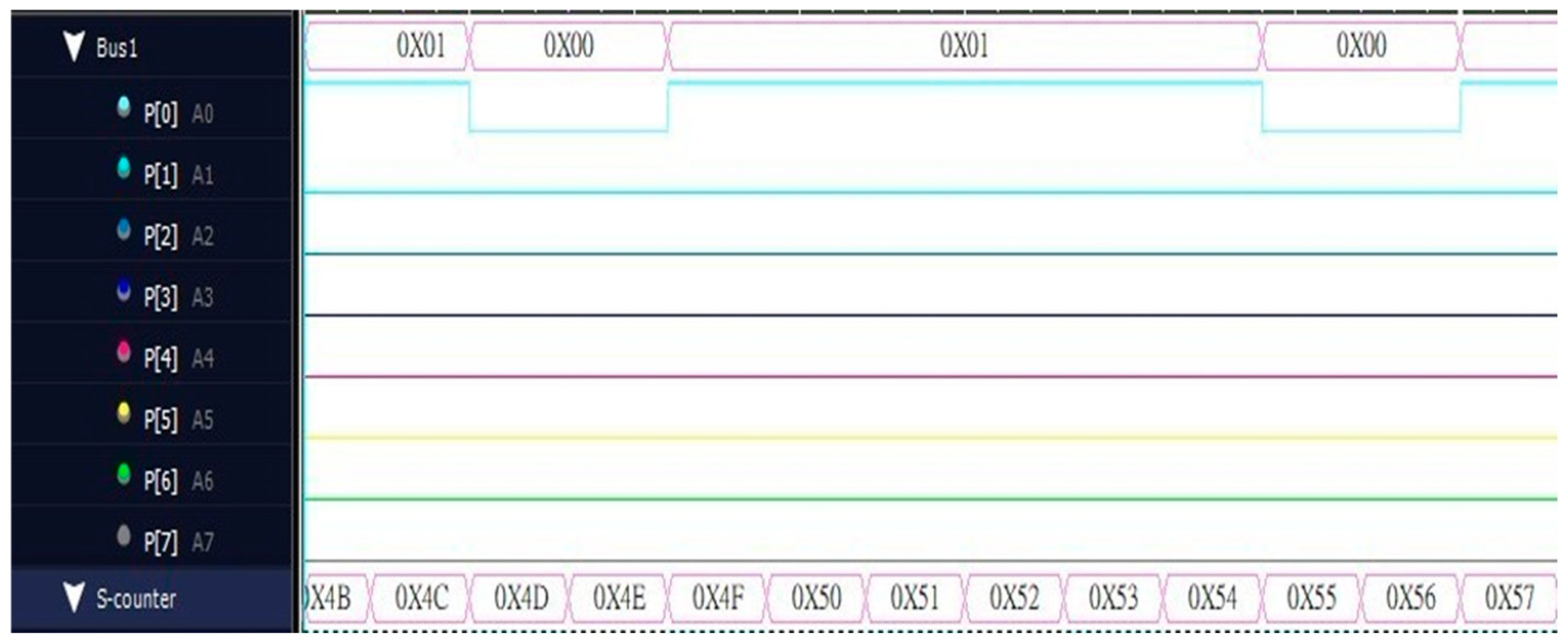
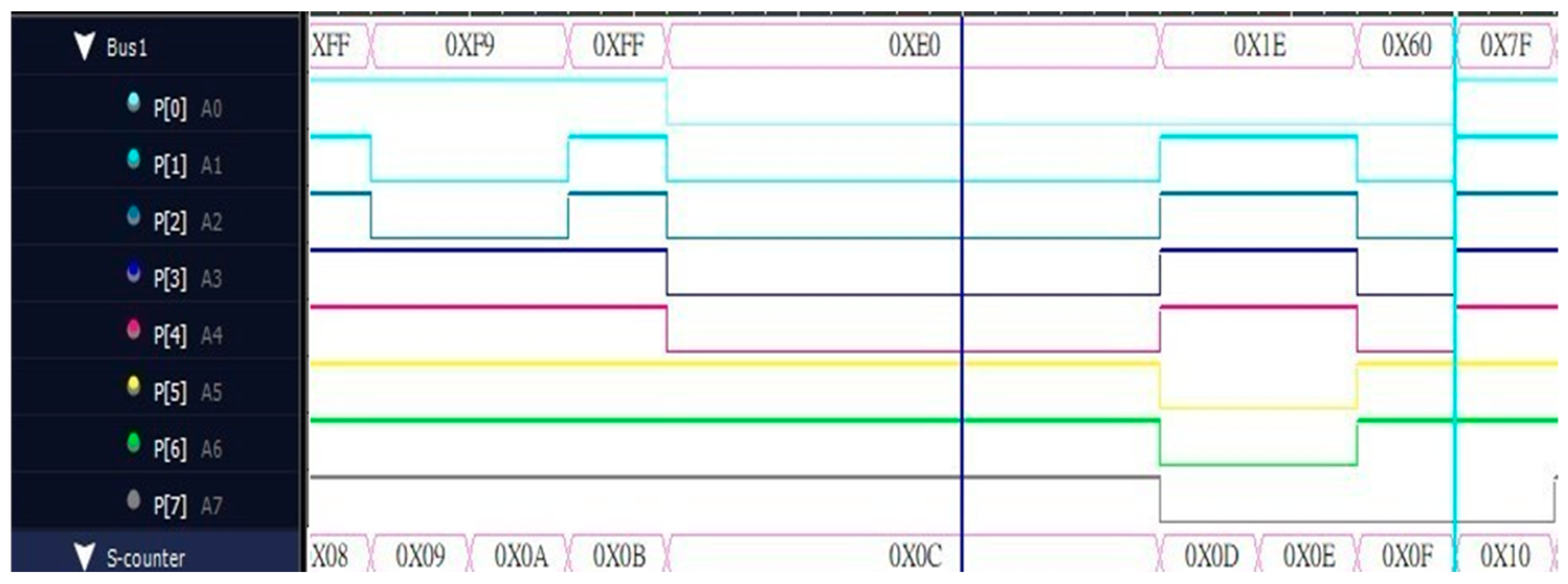
As shown in Figure 6, it is the serial output waveform captured by the logic analyzer. The developed serial output is P[0] in the output pin P[7:0] for output, and the lower half is the counter value. Therefore, the output value is regarded as a point in time.
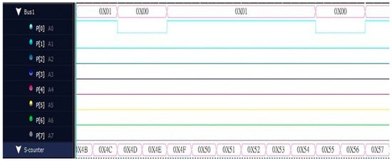
Figure 6.
Serial output diagram.
Figure 7 shows the parallel output waveform captured by the logic analyzer. The upper half synthesizes the output 8-bit value into the bus, which is more convenient when compared with the serial output, while the lower half is the counter calculation. The purpose of the numerical value is to know what the output value is at which point in time.
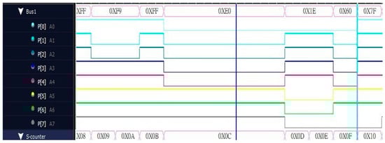
Figure 7.
Parallel output diagram.
The usage rate of components is simulated using Vivado. Except for the relatively high input-output (IO) port utilization of 17.62%, the utilization rates of other components are low. LUTs use 1.38%, FFs use 0.75%, and BUFG uses 6.25% of the usage, as shown in Table 1. The PUF design requires minimal logic resources and is highly efficient in circuits without consuming too much hardware area.

Table 1.
PUF component usage.
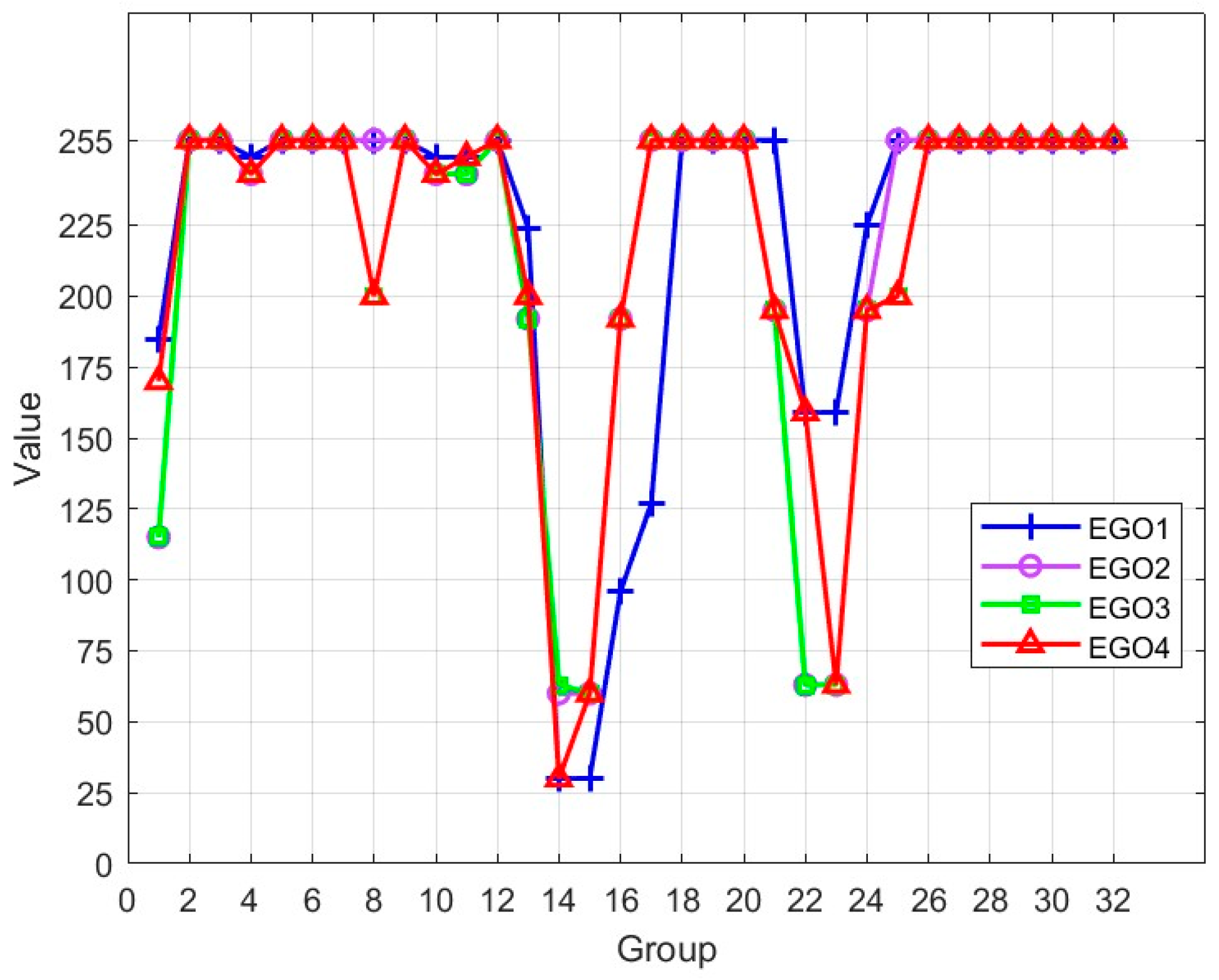
We used four EGO verification platforms for testing (EGO1–EGO4) (Figure 8). Moreover, 256 bits were divided into 32 groups of eight bits each, with each group having a numerical range of 0–255. When the application was used on different boards of the same chip, varying delay lengths caused the deviation of the output, implying that each board possesses a unique code.
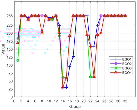
Figure 8.
PUF output comparison.
5. Conclusions
Currently, PUF experiments rely on manual operation or external signals for triggering, which is not convenient. The use of external signals increases the number of IO ports and the circuit area. To address this, we developed a circuit generating a counter, input, and reset to implement an automatic PUF generator, offering the ability to select the output mode and enhancing overall convenience.
Author Contributions
Conceptualization, K.-H.L. and W.-H.W.; methodology, K.-H.L.; software, W.-H.W.; validation, K.-H.L., W.-H.W. and I.-C.W.; formal analysis, W.-H.W.; investigation, I.-C.W.; resources, K.-H.L.; data curation, K.-H.L.; writing—original draft preparation, K.-H.L. and W.-H.W.; writing—review and editing, K.-H.L.; visualization, K.-H.L.; supervision, K.-H.L.; project administration, K.-H.L.; funding acquisition, K.-H.L. All authors have read and agreed to the published version of the manuscript.
Funding
This research was supported in part by the national science and technology council in Taiwan under grant number NSTC 113-2637-E-150-007.
Institutional Review Board Statement
Not applicable.
Informed Consent Statement
Not applicable.
Data Availability Statement
The datasets generated during and/or analyzed during the current study are available from the corresponding author on reasonable request.
Acknowledgments
This research was supported in part by technical services from Taiwan Semiconductor Research Institute (TSRI), Taiwan.
Conflicts of Interest
The authors declare no conflict of interest.
References
- Idriss, T.; Idriss, H.; Bayoumi, M. A puf-based paradigm for iot security. In Proceedings of the 2016 IEEE 3rd World Forum on Internet of Things (WFIoT), Reston, VA, USA, 12–14 December 2016; pp. 700–705. [Google Scholar]
- Alkatheiri, M.S.; Zhuang, Y.; Korobkov, M.; Sangi, A.R. An experimental study of the state-of-the-art PUFs implemented on FPGAs. In Proceedings of the 2017 IEEE Conference on Dependable and Secure Computing, Taipei, Tanwan, 7–10 August 2017; pp. 174–180. [Google Scholar]
- Lee, J.W.; Lim, D.; Gassend, B.; Suh, G.E.; Van Dijk, M.; Devadas, S. A technique to build a secret key in integrated circuits for identification and authentication applications. In Proceedings of the 2004 Symposium on VLSI Circuits, Honolulu, HI, USA, 17–19 June 2004. Digest of Technical Papers (IEEE Cat. No. 04CH37525). [Google Scholar]
- Herder, C.; Yu, M.D.; Koushanfar, F.; Devadas, S. Physical Unclonable Functions and Applications: A Tutorial. Proc. IEEE 2014, 102, 1126–1141. [Google Scholar] [CrossRef]
- Kumar, S.S.; Guajardo, J.; Maes, R.; Schrijen, G.J.; Tuyls, P. Extended abstract: The butterfly PUF protecting IP on every FPGA. In Proceedings of the 2008 IEEE International Workshop on Hardware-Oriented Security and Trust, Anaheim, CA, USA, 9 June 2008; pp. 67–70. [Google Scholar]
- Nozaki, Y.; Takemoto, S.; Ikezaki, Y.; Yoshikawa, M. Performance Evaluation of Unrolled Cipher based Glitch PUF Implemented on Virtex-7. In Proceedings of the 2021 International Symposium on Devices, Circuits and Systems (ISDCS), Higashihiroshima, Japan, 3–5 March 2021; pp. 1–4. [Google Scholar]
- Kareem, H.; Dunaev, D. Xilinx FPGA-based Ring Oscillator PUFs: Design Challenges and Solutions. In Proceedings of the 2022 11th Mediterranean Conference on Embedded Computing (MECO), Budva, Montenegro, 7–11 June 2022; pp. 1–5. [Google Scholar]
- Talukder, B.M.S.B.; Ferdaus, F.; Rahman, T. Memory-Based PUFs are Vulnerable as Well: A Non-Invasive Attack Against SRAM PUFs. IEEE Trans. Inf. Forensics Secur. 2021, 16, 4035–4049. [Google Scholar] [CrossRef]

Disclaimer/Publisher’s Note: The statements, opinions and data contained in all publications are solely those of the individual author(s) and contributor(s) and not of MDPI and/or the editor(s). MDPI and/or the editor(s) disclaim responsibility for any injury to people or property resulting from any ideas, methods, instructions or products referred to in the content. |
© 2025 by the authors. Licensee MDPI, Basel, Switzerland. This article is an open access article distributed under the terms and conditions of the Creative Commons Attribution (CC BY) license (https://creativecommons.org/licenses/by/4.0/).