Next Article in Journal
CAVE Automatic Virtual Environment Technology: A Patent Analysis
Previous Article in Journal
Algorithm Design for Multicellular Molecular Communication Simulations
 
 
engproc-logo
Article Menu

Article Menu

Proceeding Paper

Development of a High-Stability Boost Converter Using Supercapacitor Integration Using the Perturb and Observe Control Method for Photovoltaic Application †

Department Electrical Engineering, Diponegoro University, UNDIP Campus Tembalang, Jl. Prof. Soedarto, S.H., Semarang 50275, Indonesia
*
Author to whom correspondence should be addressed.
Presented at the 8th Mechanical Engineering, Science and Technology International Conference, Padang Besar, Perlis, Malaysia, 11–12 December 2024.
Eng. Proc. 2025, 84(1), 68; https://doi.org/10.3390/engproc2025084068
Published: 19 February 2025

Abstract

:
This paper aims to demonstrate the energy efficiency improvements in a boost converter using supercapacitors and the Perturb and Observe (PO) control method, particularly in the context of photovoltaic (PV) systems under partial shading conditions. Supercapacitors, known for their high energy density and rapid charge/discharge capabilities, are integrated into the boost converter circuit to mitigate voltage fluctuations and enhance energy storage efficiency. The PO control method is utilized to dynamically adjust the duty cycle of the MOSFET, ensuring the output voltage remains stable at the desired level of 70 V, with an input voltage range of 30 V to 60 V. This study employs simulation techniques to evaluate performance improvements, focusing on energy efficiency and system stability when supercapacitors are used as filtering elements alongside advanced control strategies in PV systems experiencing partial shading. Simulation results indicate a significant reduction in voltage ripple and enhanced overall system efficiency, achieving a stable output voltage of exactly 70 volts. Specifically, the efficiency of the boost converter without a supercapacitor and Zener diode is 8.36%, while the configuration with a supercapacitor and Zener diode achieves 16.09% efficiency. Most notably, the configuration with a supercapacitor and without a Zener diode achieves an efficiency of 50.29%. The findings conclude that integrating supercapacitors and the PO control method in boost converters for PV applications substantially enhances energy efficiency and system stability, even under partial shading conditions.

1. Introduction

Solar panels are essential components for generating electricity from sunlight [1]. This renewable energy source is highly favored because it can convert natural energy into electrical energy for daily activities [2]. However, solar panels cannot operate independently; they require additional components such as maximum power point trackers (MPPTs), batteries, and inverters [3]. A boost converter is employed to increase the voltage so that the power output remains within specifications when delivered by the inverter. In a boost converter, pulse width modulation (PWM) signal control is required to increase the voltage using a control method to achieve the desired set-point and provide an optimal PWM signal [4].
In this research, the boost converter’s design is modified by replacing the traditional filter capacitor with a supercapacitor [5]. This change aims to achieve a more stable output, ensuring the generated power can be optimized without excessive power loss during the voltage boosting process. Additionally, one of the key challenges in photovoltaic systems is partial shading, where portions of the solar panel array receive less sunlight due to obstructions such as clouds, trees, or buildings. Partial shading can cause significant fluctuations in the output voltage, leading to reduced efficiency and power losses. Traditional boost converters struggle to maintain voltage stability under these conditions, often resulting in suboptimal performance.
Existing boost converter designs often experience ripple in the output voltage, which can lead to power loss and instability for devices connected downstream. This paper proposes a new boost converter design that incorporates supercapacitors in place of conventional capacitors. The effectiveness of this new design is evaluated through simulations to compare its performance with traditional designs, especially under partial shading conditions. While previous studies have explored various methods to reduce voltage ripple and improve stability, including the use of advanced control algorithms and alternative passive components, the use of supercapacitors as a replacement for conventional capacitors in boost converters has not been extensively studied, particularly in the context of partial shading.
This research uniquely demonstrates that integrating supercapacitors not only enhances voltage stability but also significantly outperforms existing designs in terms of reducing voltage ripple and minimizing energy losses, even under partial shading conditions. By providing a comprehensive comparison with established methods, this study offers a novel approach that can be effectively utilized in practical applications, paving the way for more reliable and efficient energy systems [6].
Furthermore, while the integration of supercapacitors with Perturb and Observe (P&O) control is a well-established technique in the literature, there remains a notable gap in addressing the specific challenges of system stability and energy optimization when combining supercapacitors with advanced control methods. This study contributes to filling this gap by showcasing the potential benefits of this integration. It highlights how combining supercapacitors with P&O control not only improves voltage regulation and system performance but also optimizes the overall power output, particularly in dynamic and challenging conditions such as partial shading. Through this approach, the paper introduces a novel and effective solution to enhance the stability and efficiency of photovoltaic boost converter systems.

2. Literature Review

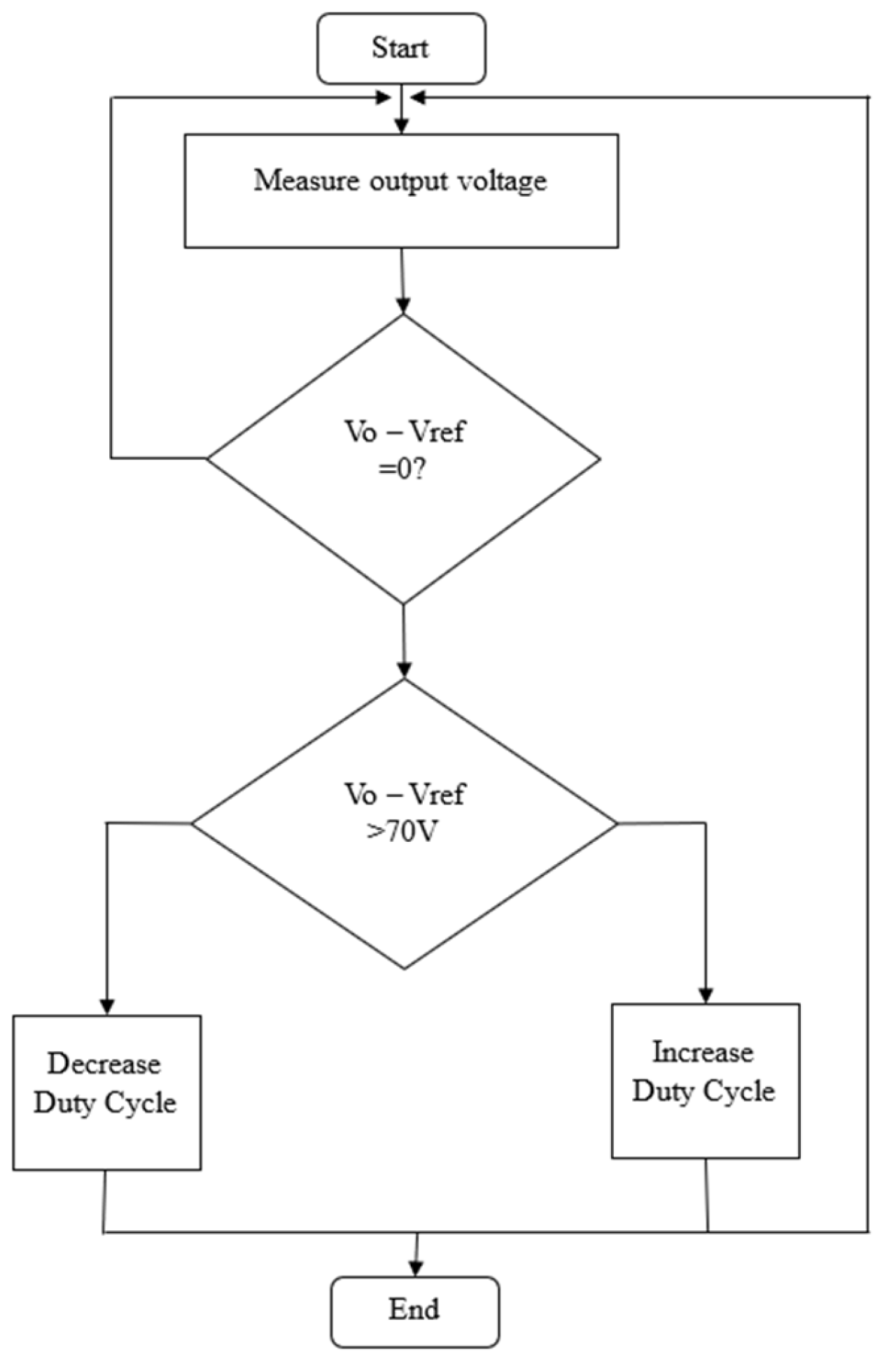
2.1. Perturb and Observe (PO) Method

The Perturb and Observe (PO) method is straightforward to apply. However, in its operation, this method has power losses due to the constant fluctuation of the Maximum Power Point (MPP) value [7]. Some reference sources explain the shortcomings of using this method, including the fact that the performance of PO does not provide a stable response with changes in irradiance levels [8]. The Perturb and Observe (PO) algorithm operates by periodically perturbing the PV voltage by varying the duty cycle and observing the PV power to increase or decrease the PV voltage in the next cycle [9]. This algorithm works to move the operating point both positively and negatively to always be at the maximum point. The algorithm requires the power, voltage, and current parameter values from the PV system as its inputs. This method works by perturbing (increasing or decreasing) the duty cycle, as illustrated in Figure 1 [10]. Each time the duty cycle changes, the change in power is observed. If the current power is greater than the previous power, then the duty cycle will be increased further. If the current power is less than the previous power, then the duty cycle will be decreased. Therefore, this method requires input values of the output power to determine the power delivered to the load.

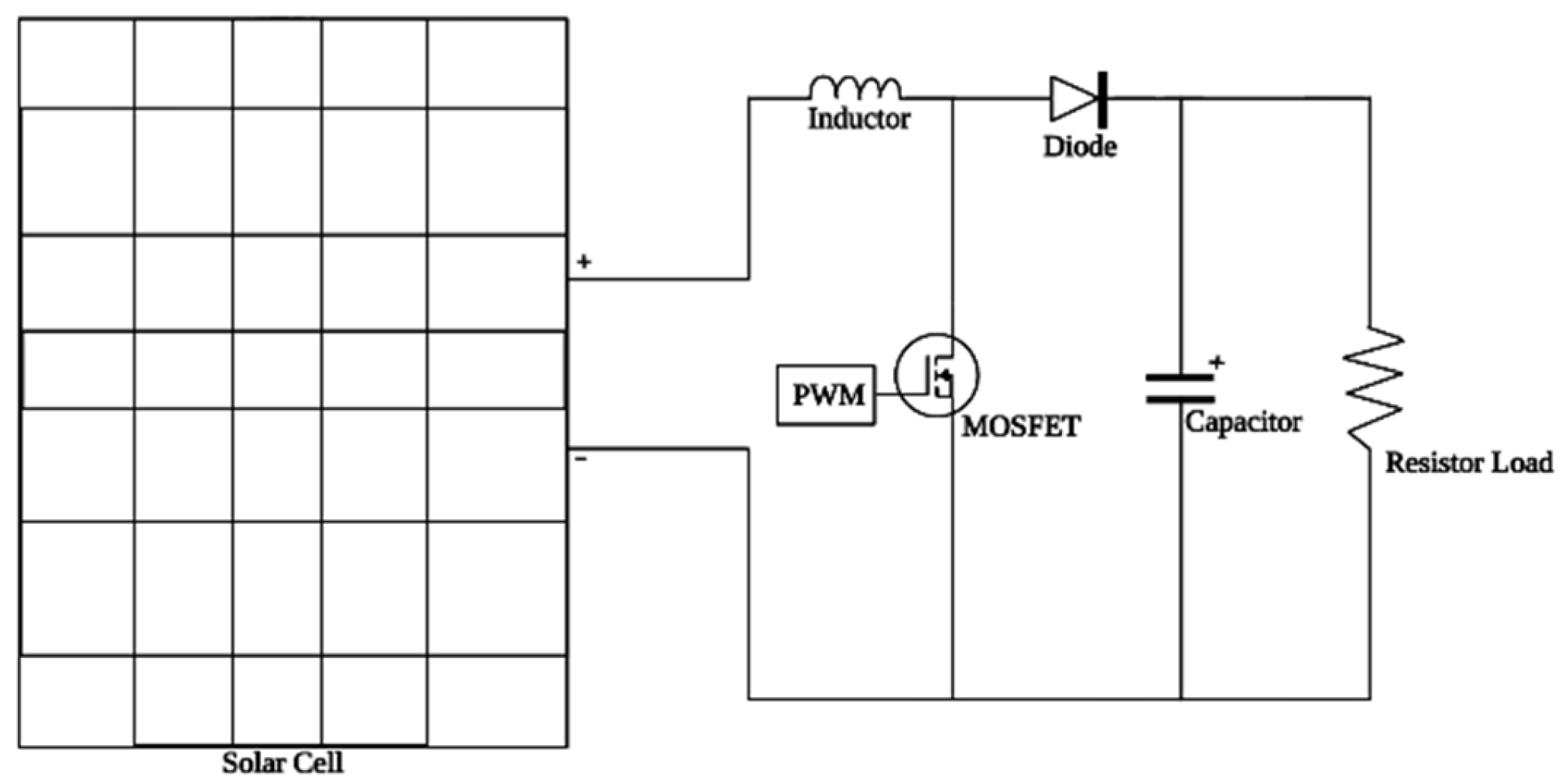
2.2. Boost Converter

The boost converter is a DC-DC voltage step-up circuit. The output voltage value can be increased by changing the duty cycle value in the switching of the boost converter circuit [11]. One application of the boost converter circuit is in photovoltaic (PV) systems connected to the grid. The PV voltage is increased using the boost converter until it reaches a sufficient voltage level as the input voltage for the inverter [12]. Subsequently, the inverter converts the DC voltage into AC voltage to be connected to the grid. As shown in Figure 2, the boost converter is connected to the solar panel for its source.
In this research, we compare systems with and without supercapacitors [13]. The system with a supercapacitor can be seen in Figure 3 Some supercapacitors cannot receive voltage above their specifications, so we compare the supercapacitor with and without a Zener diode, as shown in Figure 3 and Figure 4. However, the difference is not significant, so it is tolerable for the supercapacitor to work with the voltage provided by the boost converter. Figure 3 shows the system without a supercapacitor. Both systems, with and without supercapacitors, will receive feedback from the output to be optimized by the PO control method, ensuring the output remains at 70 V.
The components that make up a boost converter include the following:

2.2.1. Solar Panels

The power sources for the circuit are solar panels, while batteries are used to supply power to the PWM control circuit and MOSFET driver.

2.2.2. Switch

The switching component used is the MOSFET. The selection of the MOSFET considers the voltage and current values of the converter. The MOSFET used is the IRFP4242PbF, which has a drain-source voltage (VDS) of 300 volts and a maximum drain current (ID) of 46 amperes. The IRFP4242PbF MOSFET is safe to use because the desired output voltage is 70 VDC, and the maximum supply current is 14.28 A.

2.2.3. Diode

The diode used is the NTE5826. This diode is chosen because it is designed for high power applications. The NTE5826 diode has a maximum voltage capability of 400 volts and a current rating of up to 50 amperes, making it safe to use in the boost converter.

2.2.4. Inductor

The inductor used is a solenoidal inductor made from copper wire wound around a ferrite core. The inductance can be calculated using the following equation:
L m i n = D m i n 1 D m i n 2 R 2 f
= 0.1 1 0.9 2 × 400 2 × 1000
= 16.2   m H
In Continuous Conduction Mode (CCM), the inductance created must be greater than the minimum inductance. Therefore, the inductance used is 30 mH.

2.2.5. Capacitor

The capacitor functions as a filter to limit the output voltage ripple of the converter. The capacitor used in the design of this boost converter has a ripple of 1%. The capacitance value can be calculated using the following equation:
C m i n = D m a x % V r × R × f
= 90 % 1 % × 400 × 1000
= 0.9 0.01 × 400 × 1000
= 225   μ F
This converter is widely used for solar power generation and wind turbine applications [14]. Its main components consist of MOSFETs, diodes, inductors, and capacitors. When the MOSFET switch is closed, current flows through the inductor, causing the energy stored in the inductor to increase [15]. When the MOSFET switch is open, the current from the inductor flows to the load through the diode, causing the energy stored in the inductor to decrease. The ratio between the output voltage and the input voltage of the converter is proportional to the ratio between the switching period and the switch-off time.

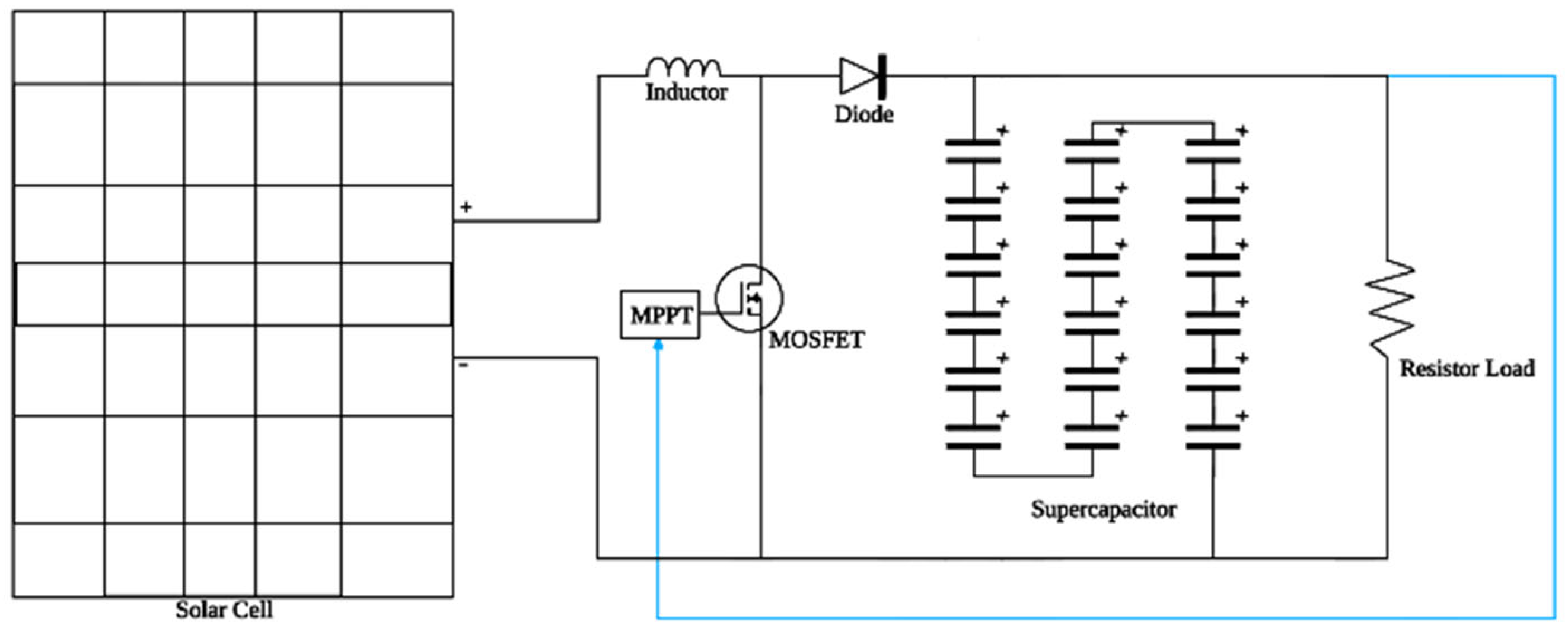
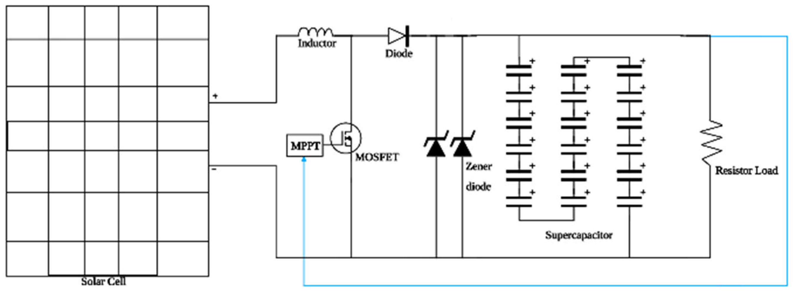
2.2.6. Supercapacitor
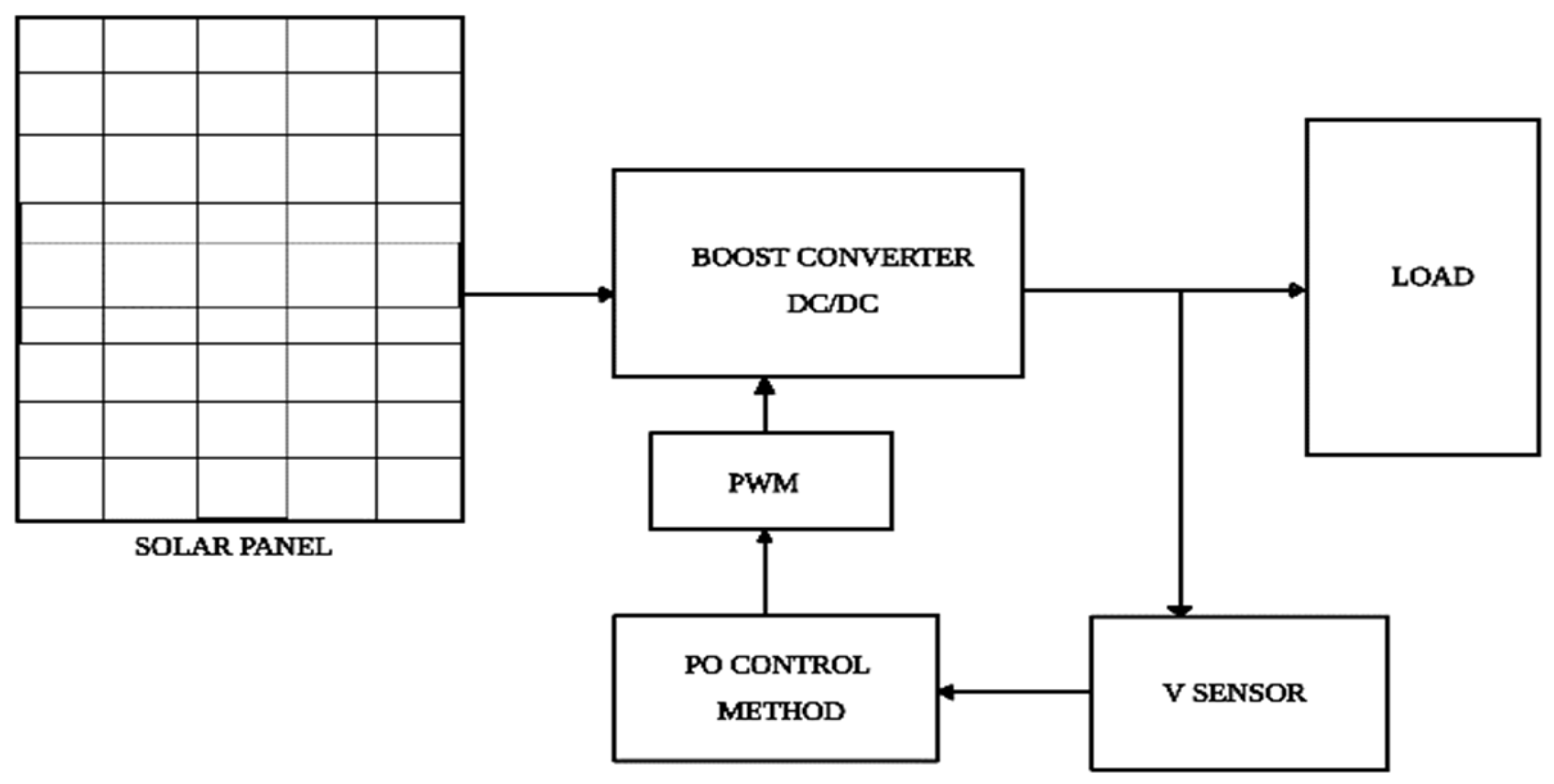
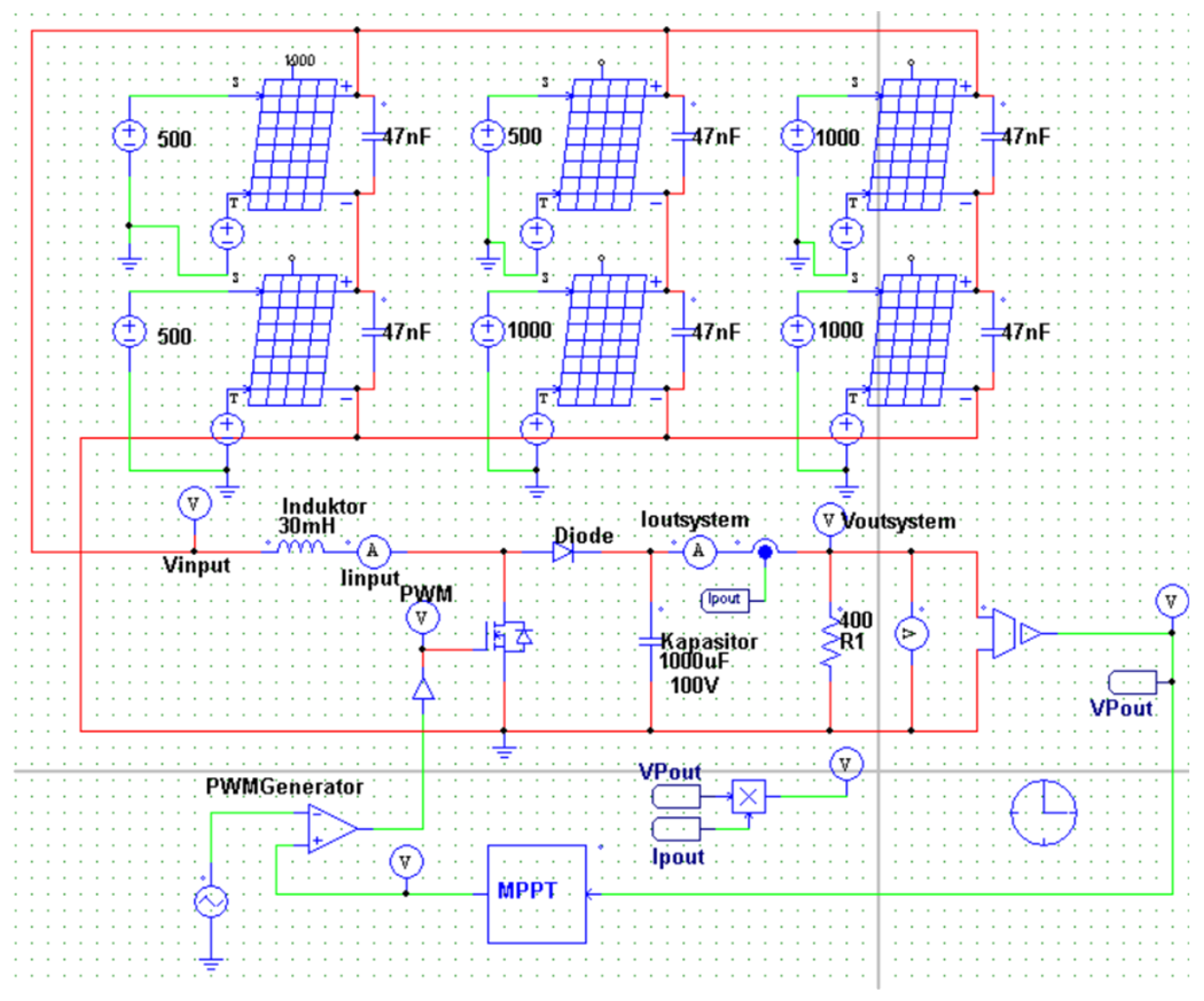
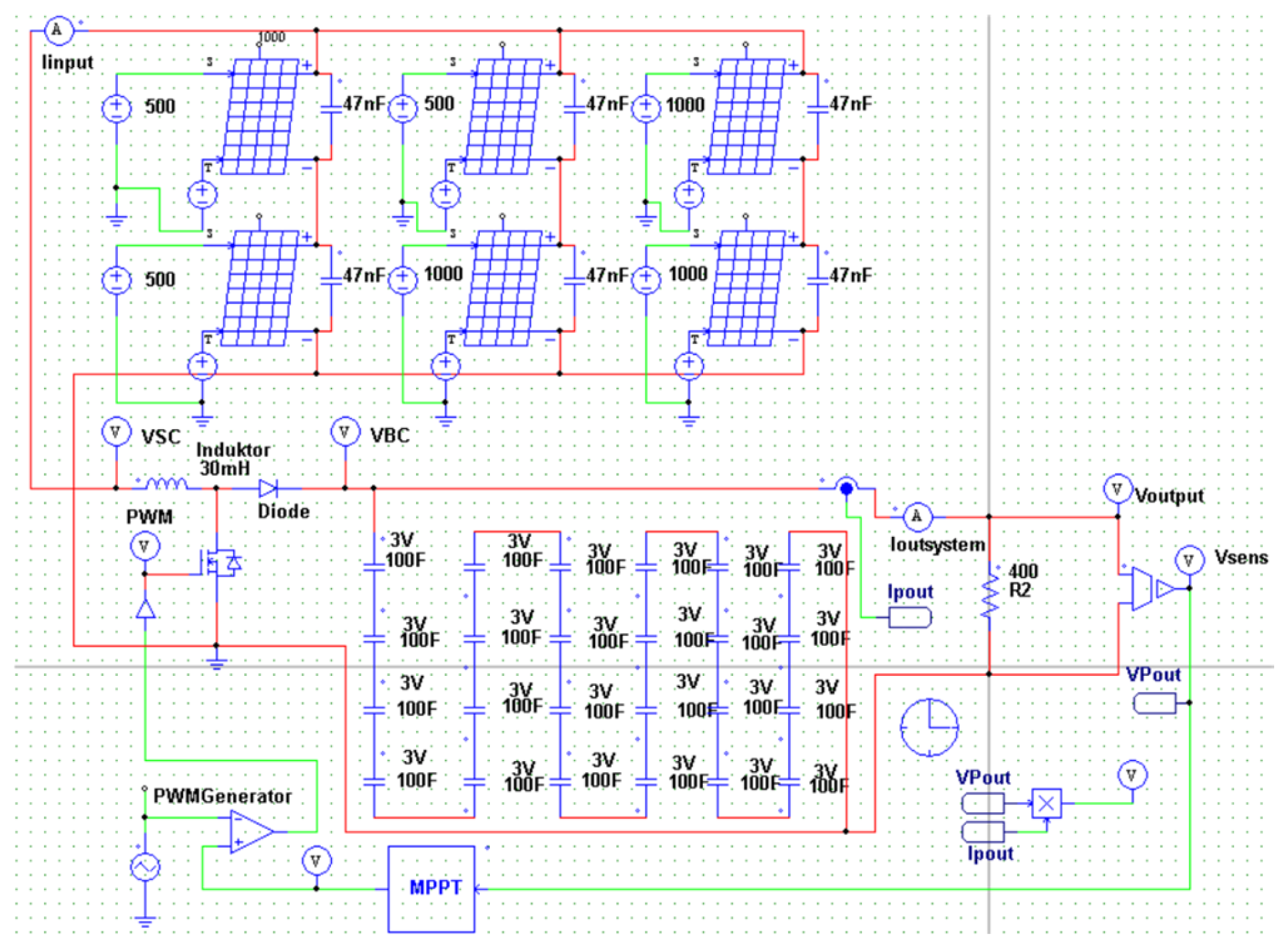
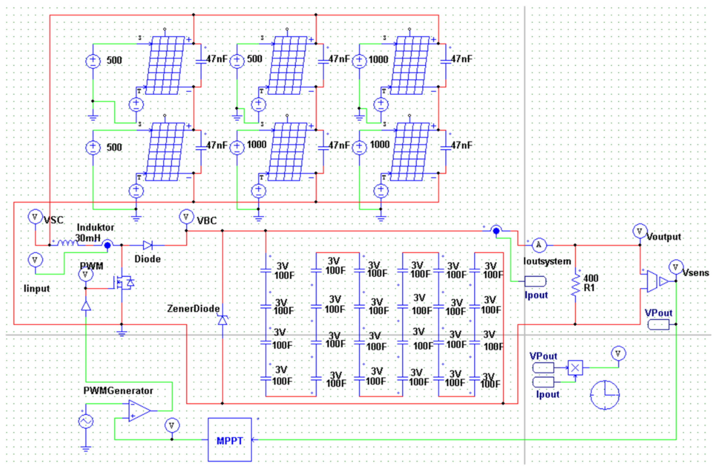
The supercapacitor is used as a replacement for a capacitor. Both the supercapacitor and the capacitor have the same function, which is to filter the output that will be delivered from the boost converter [16]. The difference between a supercapacitor and a regular capacitor lies in their operational durability and stability in providing output [17]. The supercapacitor used in this research has a working voltage of 3 volts and a capacitance of 100 F and can deliver a current of 11.7 A. Since no supercapacitor specification can provide a voltage of 100 V, the supercapacitors will be connected in series to achieve a working voltage of 70 V. A total of 24 supercapacitors will be connected in series to achieve a working voltage of 70 V as per the desired specifications.

3. System Design

Simulation Design

Block diagram of simulation for system can be seen in Figure 5 below.
The simulation of the system is conducted using the software with the specifications of the solar panel, as shown in Table 1. The values of the components used in the system are calculated using formulas, such as those for the inductor and capacitor. These formulas aim to determine not the exact value of the component, but the minimum value required to ensure the system operates according to the desired specifications without unnecessarily increasing the component size, as detailed in Table 2.

4. Result and Analysis

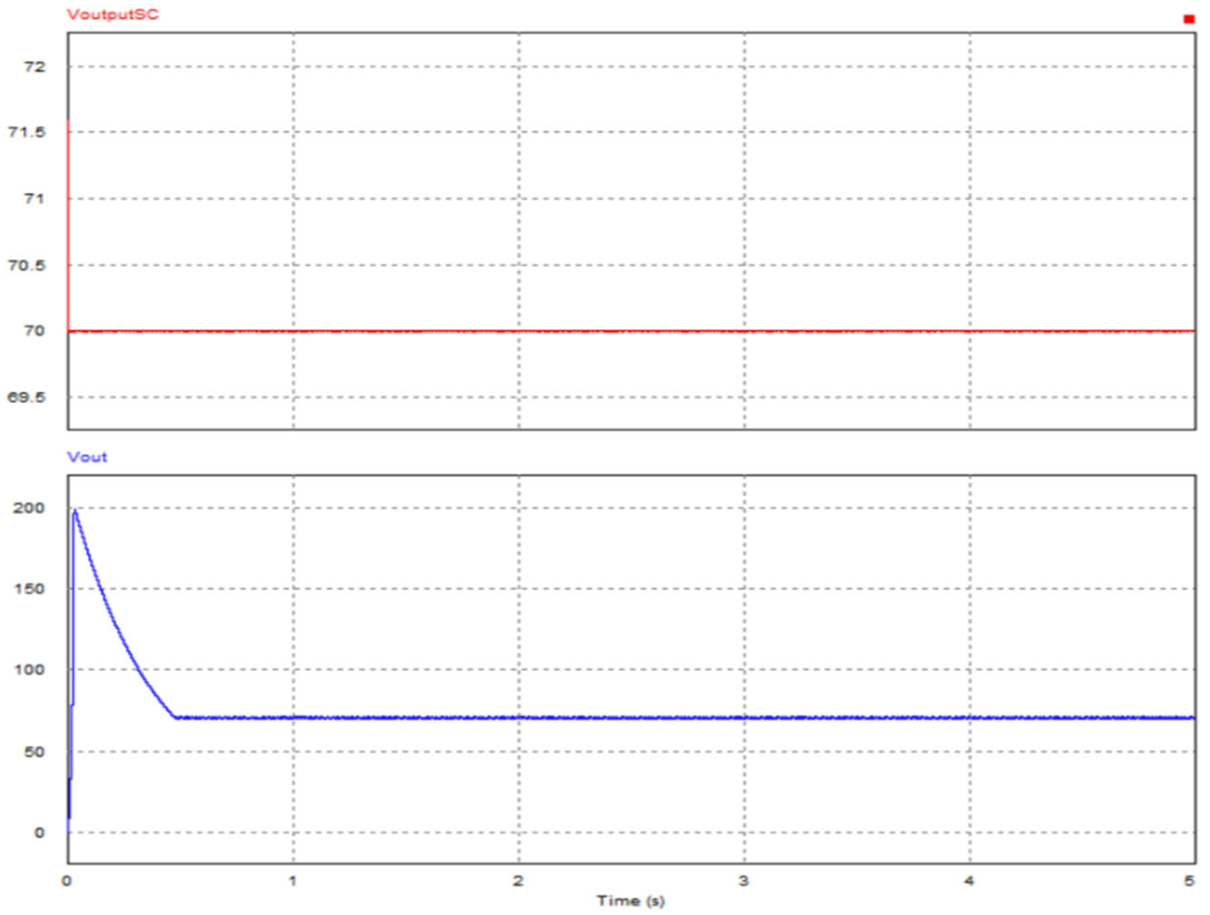
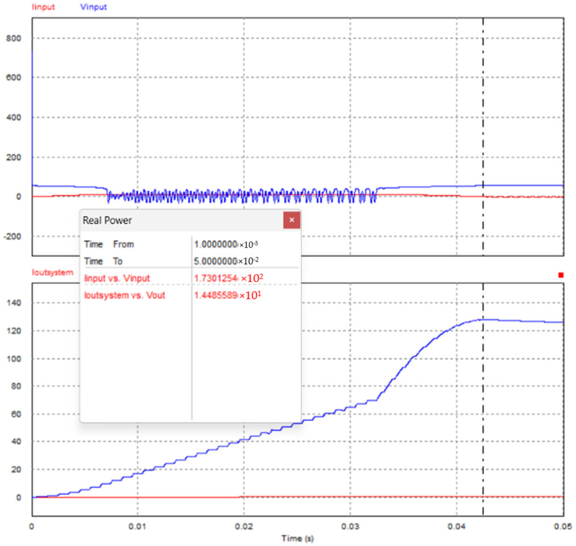
4.1. Simulation Result

Boost converter system simulation was performed by measuring the output voltage of the boost converter and the ripple that occurred on the output. The circuit diagram of the boost converter used to simulate the system can be seen in Figure 6.
Figure 6 illustrates the schematic of a boost converter, detailing the critical components and their operational interaction. The converter functions by stepping up the input voltage, storing energy in the inductor during the switch-on phase, and releasing it during the switch-off phase, thereby achieving a higher output voltage. This elevated voltage is essential for the efficient charging of the supercapacitor and for meeting the voltage requirements of downstream circuits.
Figure 7 presents the configuration of a boost converter integrated with a supercapacitor, demonstrating the process of voltage step-up and subsequent energy storage. The converter efficiently charges the supercapacitor by elevating the input voltage, thereby enhancing energy storage capability and ensuring a stable power supply to the load during periods of increased demand.
This figure presents the configuration of a boost converter integrated with a supercapacitor, demonstrating the process of voltage step-up and subsequent energy storage. The converter efficiently charges the supercapacitor by elevating the input voltage, while a Zener diode is incorporated to limit the output voltage to 70 V, thereby enhancing energy storage capability and ensuring a stable power supply to the load during periods of increased demand. The simulation output voltage will be mainly observed to see and compare the output between with and without a supercapacitor and to test the output with feedback with optimization using the PO method. The results of the simulation can be seen in Figure 8.
In Figure 9, there are two outputs: the red curve is the boost converter with a supercapacitor and the blue curve is the boost converter without a supercapacitor. A Zener diode is used in the boost converter with a supercapacitor.
In Figure 10, there are two output curves: the blue curve is the boost converter without a supercapacitor, and the red curve is the boost converter with a supercapacitor without a Zener diode.
Figure 11 shows different results of the simulation, which is a blue graph for a conventional boost converter, a red graph for the boost converter with supercapacitor integration, and a green graph for the boost converter with supercapacitor integration and a Zener diode.
Figure 12 shows graphs of the input and output voltage, current, and power values. The power values are used to calculate efficiency, as depicted in Figure 12. The efficiency can be calculated using the following equation:
η = P o u t P i n × 100 %
η = 14.48 173.01 × 100 %
η = 8.36 %
Figure 13 shows graphs of the input and output voltage, current, and power values. The power values are used to calculate efficiency, as depicted in Figure 13. The efficiency can be calculated using the following equation:
η = P o u t P i n × 100 %
η = 12.96 25.77 × 100 %
η = 50.29 %
Figure 14 shows graphs of the input and output voltage, current, and power values. The power values are used to calculate efficiency, as depicted in Figure 14. The efficiency can be calculated using the following equation:
η = P o u t P i n × 100 %
η = 12.25 76.09 × 100 %
η = 16.09 %

4.2. Analysis

The simulation results of the boost converter using two different components show the voltage output waveform simulated with the Perturb and Observe (PO) method algorithm. The simulation was conducted with an irradiance value of 1000 W/m2 and 500 W/m2 to mimic partial shading with the temperature set at 25 °C. Figure 10, Figure 11 and Figure 12 illustrate that the PO method effectively tracks the desired 70 Vdc voltage. By dynamically adjusting the duty cycle of the pulse width modulation (PWM) signal for the MOSFET gate, the PO method ensures the output voltage remains stable at 70 volts, as intended.
Analysing the simulation results for each circuit reveals that both configurations reach the desired voltage of 70 volts. However, the output signals and efficiencies differ between the circuits. In the boost converter without a supercapacitor (Figure 12), the signal exhibits voltage ripple at the output, and the overall efficiency is relatively low at 8.36%, as shown in Table 3. This inefficiency is due to the ripple causing power losses and instability, which negatively affect the performance of the system.
In contrast, the boost converter with a supercapacitor and a Zener diode (Figure 14) reaches 70 volts without any ripple, resulting in a slightly improved efficiency of 16.09%, as shown in Table 3. This stability is due to the voltage regulator diode (Zener diode), which maintains the output voltage at 70 volts. Although ripple can still occur with a Zener diode, Figure 14 shows a stable signal at 70 volts, contributing to the improved, albeit modest, efficiency.
Most notably, in the boost converter with a supercapacitor but without a Zener diode (Figure 14), the output voltage gradually decreases from 72 volts to 70 volts. While no ripple is present, the output voltage initially exceeds the desired design. This occurs because the boost converter’s cycle is too fast, causing the supercapacitor to store voltage at 72 volts, which then slowly decreases as the duty cycle decreases, until reaching the optimal value of 70 volts. Despite this initial overshoot, this configuration achieves a significantly higher efficiency of 50.29%, as shown in Table 3. The absence of ripple and the efficient energy storage capability of the supercapacitor contribute to this remarkable improvement, demonstrating the potential of supercapacitor integration in enhancing boost converter performance.
Figure 12, Figure 13 and Figure 14 present the power comparison of input versus output for the three configurations, providing further insight into the efficiency percentages. The data show that the configuration without a supercapacitor and without a Zener diode exhibits significant power losses, with a low output-to-input power ratio, corresponding to its 8.36% efficiency, as shown in Table 3. The configuration with a supercapacitor and Zener diode shows a modest improvement in power output, leading to its 16.09% efficiency, as shown in Table 3. The most efficient configuration, with a supercapacitor and without a Zener diode, demonstrates the highest output-to-input power ratio, corresponding to its 50.29% efficiency, as shown in Table 3. These data confirm that the supercapacitor’s role in reducing power losses and enhancing voltage stability is crucial for optimizing boost converter performance.
In summary, the analysis reveals that while both configurations achieve the desired output voltage, the use of a supercapacitor, particularly without a Zener diode, provides substantial benefits in terms of efficiency and voltage stability. The configuration with a supercapacitor and without a Zener diode stands out with efficiency of 50.29%, as shown in Figure 14 and Table 3, far surpassing the other configurations, making it the most effective design for minimizing power losses and optimizing energy conversion in boost converters.

5. Conclusions

The simulation results of the boost converter, evaluated under varying conditions of irradiance and temperature, demonstrate the effectiveness of the Perturb and Observe (PO) method in maintaining a stable output voltage of 70 Vdc. While both configurations—one with a supercapacitor and one without—achieve the desired output, the inclusion of a supercapacitor proves to be a key factor in improving the converter’s efficiency and voltage stability.
The configuration without a supercapacitor exhibited significant voltage ripple and low efficiency (8.36%) due to power losses associated with the ripple. In contrast, the configuration with a supercapacitor and Zener diode displayed improved voltage stability and a modest increase in efficiency (16.09%), with the Zener diode helping to regulate the output voltage. However, the most notable performance improvement occurred in the configuration with a supercapacitor but without a Zener diode, which achieved impressive efficiency of 50.29%. This setup eliminated voltage ripple, and the supercapacitor’s energy storage capability enabled more efficient power conversion, contributing to its superior performance.
The power comparison further confirms that the supercapacitor plays a crucial role in reducing power losses and enhancing voltage stability. Therefore, the configuration with a supercapacitor, particularly without the Zener diode, represents the most effective design, offering the highest efficiency and demonstrating significant potential for optimizing boost converter performance in practical applications.

Author Contributions

Conceptualization, I.H.; methodology, I.H.; software, I.H.; validation, D. and I.S.; writing—original draft preparation, I.H.; writing—review and editing, I.H., D. and I.S.; supervision, D. and I.S. All authors have read and agreed to the published version of the manuscript.

Funding

This research received no external funding.

Institutional Review Board Statement

Not applicable.

Informed Consent Statement

Not applicable.

Data Availability Statement

The data that support the findings of this study are available from the corresponding author upon reasonable request.

Acknowledgments

The authors would like to thank the Department of Electrical Engineering for assistance in the process of research and writing this paper.

Conflicts of Interest

The authors declare no conflicts of interest.

References

  1. Soedibyo; Amri, B.; Ashari, M. The Comparative Study of Buck_Boost, Cuk, Sepic and Zeta Converters for Maximum Power Point Tracking Photovoltaic Using P&O Method. In Proceedings of the 2015 2nd International Conference on Information Technology, Computer, and Electrical Engineering (ICITACEE), Semarang, Indonesia, 16–18 October 2015; pp. 327–332. [Google Scholar]
  2. Agrawal, A.; Gupta, R. Optimized sensor charge controller for bus voltage stabilization in hybrid battery-supercapacitor fed islanded microgrid system. J. Energy Storage 2023, 59, 106482. [Google Scholar] [CrossRef]
  3. Alam, M.A.; Minai, A.F.; Bakhsh, F.I. Isolated Bidirectional DC-DC Converter: A Topological Review. e-Prime-Adv. Electr. Eng. Electron. Energy 2024, 8, 100594. [Google Scholar] [CrossRef]
  4. Anshory, I.; Jamaaluddin, J.; Wisaksono, A.; Sulistiyowati, I.; Rintyarna, B.S.; Fudholi, A.; Fudholi, A.; Rahman, Y.A.; Sopian, K. Optimization DC-DC boost converter of BLDC motor drive by solar panel using PID and firefly algorithm. Results Eng. 2024, 21, 101727. [Google Scholar] [CrossRef]
  5. Mousa, H.H.H.; Youssef, A.R.; Mohamed, E.E.M. State of the art perturb and observe MPPT algorithms based wind energy conversion systems: A technology review. Int. J. Electr. Power Energy Syst. 2021, 126, 106598. [Google Scholar] [CrossRef]
  6. Assyidiq, M.A.; Winardi, B.; Andromeda, T. Perancangan Boost Converter Menggunakan Voltage Feedback Pada Panel Surya. Transient 2017, 6, 404. [Google Scholar] [CrossRef]
  7. Benyahia, N.; Denoun, H.; Badji, A.; Zaouia, M.; Rekioua, T.; Benamrouche, N.; Rekioua, D. MPPT controller for an interleaved boost dc-dc converter used in fuel cell electric vehicles. Int. J. Hydrogen Energy 2014, 39, 15196–15205. [Google Scholar] [CrossRef]
  8. Powade, R.; Bhateshvar, Y. Design of semi-actively controlled battery-supercapacitor hybrid energy storage system. Mater. Today Proc. 2023, 72, 1503–1509. [Google Scholar] [CrossRef]
  9. Li, Q.; Huangfu, Y.; Xu, L.; Wei, J.; Ma, R.; Zhao, D.; Gao, F. An Improved Floating Interleaved Boost Converter with the Zero-Ripple Input Current for Fuel Cell Applications. IEEE Trans. Energy Convers. 2019, 34, 2168–2179. [Google Scholar] [CrossRef]
  10. Chincholkar, S.H.; Jiang, W.; Chan, C.Y. A Modified Hysteresis-Modulation-Based Sliding Mode Control for Improved Performance in Hybrid DC-DC Boost Converter. IEEE Trans. Circuits Syst. II Express Briefs 2018, 65, 1683–1687. [Google Scholar] [CrossRef]
  11. Dandil, B.; Acikgoz, H.; Coteli, R. An effective MPPT control based on machine learning method for proton exchange membrane fuel cell systems. Int. J. Hydrogen Energy 2024, 75, 344–353. [Google Scholar] [CrossRef]
  12. González, A.; López-Erauskin, R.; Gyselinck, J. Analysis, modeling, control and operation of an interleaved three-port boost converter for DMPPT systems including PV and storage at module level. Heliyon 2019, 5, e01402. [Google Scholar] [CrossRef] [PubMed]
  13. Lencwe, M.J.; Olwal, T.O.; Chowdhury, S.D.; Sibanyoni, M. Nonsolitary two-way DC-to-DC converters for hybrid battery and supercapacitor energy storage systems: A comprehensive survey. Energy Rep. 2024, 11, 2737–2767. [Google Scholar] [CrossRef]
  14. Jamadar, N.M.; Jadhav, H.T. Effectiveness of supercapacitor during braking operation of electric vehicle. Mater. Today Proc. 2022, 56, 314–319. [Google Scholar] [CrossRef]
  15. Javed, U.; Veerachary, M. Battery-integrated ZVT boost converter based stand-alone PV system. Int. J. Electr. Power Energy Syst. 2024, 155, 109633. [Google Scholar] [CrossRef]
  16. Junaid, K.M.; Sukhi, Y.; Anjum, N.; Jeyashree, Y.; Ahamed, A.F.; Debbarma, S.; Chaudhary, G.; Priyadarshini, S.; Shylashree, N.; Garg, S.; et al. PV-based DC-DC buck-boost converter for LED driver. e-Prime-Adv. Electr. Eng. Electron. Energy 2023, 5, 100271. [Google Scholar] [CrossRef]
  17. Mian, S.H.; Nazir, M.S.; Ahmad, I.; Khan, S.A. Optimized nonlinear controller for fuel cell, supercapacitor, battery, hybrid photoelectrochemical and photovoltaic cells based hybrid electric vehicles. Energy 2023, 283, 129121. [Google Scholar] [CrossRef]
Figure 1. Flowchart of PO method.
Engproc 84 00068 g001
Figure 2. Boost converter circuit.
Engproc 84 00068 g002
Figure 3. Boost converter with supercapacitor integration.
Engproc 84 00068 g003
Figure 4. Boost converter circuit with supercapacitor and Zener diode integration.
Engproc 84 00068 g004
Figure 5. Block diagram of boost converter system.
Engproc 84 00068 g005
Figure 6. Boost converter before supercapacitor integration.
Engproc 84 00068 g006
Figure 7. Boost converter with integration supercapacitor.
Engproc 84 00068 g007
Figure 8. Boost converter with supercapacitor integration and Zener diode as voltage limiter.
Engproc 84 00068 g008
Figure 9. Voltage output of the boost converter with supercapacitor integration and Zener diode (red) and without supercapacitor (blue).
Engproc 84 00068 g009
Figure 10. Voltage output of boost converter without supercapacitor (blue) and with supercapacitor (red).
Engproc 84 00068 g010
Figure 11. Output of three different methods.
Engproc 84 00068 g011
Figure 12. Voltage graph and current of input and output of boost converter without supercapacitor integration.
Engproc 84 00068 g012
Figure 13. Voltage graph and current graph of input and output of boost converter with supercapacitor integration.
Engproc 84 00068 g013
Figure 14. Voltage graph and current graph of input and output of boost converter with supercapacitor integration and Zener diode.
Engproc 84 00068 g014
Table 1. Specification of solar panel.
SpecificationValue
Number of solar cell36
Maximum power (Pmax)1000 Wp
Maximum voltage (Vmax)18 V
Open circuit voltage (Voc)21.8 V
Short circuit current (Isc)6.05 A
Maximum current (Imax)5.56 A
Table 2. Boost converter specification.
SpecificationValue
Input voltage20–72 Vdc
Trigger frequency1 Khz
Duty cycle10–90%
Load resistance400 Ω
Inductor30 mH
Capacitor300 µF
Output voltage70 V
Output power1000 W
Table 3. Efficiency value between methods.
MethodsEfficiency
Boost converter before supercapacitor integration8.36%
Boost converter after supercapacitor integration50.29%
Boost converter after supercapacitor integration and with Zener diode as voltage limiter16.09%
Disclaimer/Publisher’s Note: The statements, opinions and data contained in all publications are solely those of the individual author(s) and contributor(s) and not of MDPI and/or the editor(s). MDPI and/or the editor(s) disclaim responsibility for any injury to people or property resulting from any ideas, methods, instructions or products referred to in the content.

