Abstract
Nanocrystalline CuO-ZnO composite thin films were obtained by solid-phase pyrolysis with different molar ratios of Cu:Zn (1:99 and 5:95). X-ray diffraction analysis showed that the films are composed of two phases. According to scanning electron microscopy data, the film is solid and is formed by crystallites with an average size of 18 nm. The films have high transparency in the visible range.
1. Introduction
One of the promising areas in modern chemistry is the development of multifunctional film materials with specific physical and chemical characteristics. Zinc oxide is attracting particular attention due to its properties as an n-type semiconductor with a wide band gap (Eg = 3.37 eV) [1]. Materials based on it are used in the production of optical devices [2], varistors [3], and solar cells [4].
The synthesis of thin films is achieved by various methods, such as pulsed laser deposition [5], sol–gel [6], radio frequency magnetron sputtering [7], and spray pyrolysis [8]. It has been established that the formation of a p-n heterojunction through the doping of zinc oxide with materials having p-type conductivity, such as Co3O4, CuO, and NiO, can lead to the creation of a photosensitive resistive materials [9,10].
Such materials also make it possible to obtain photodiodes with good performance. Thus, paper [11] reports on the production of ZnO:Cu (n-CZO) thin films by pulsed laser deposition on silicon with p-type conductivity (p-Si). It was found that when exposed to visible light, the photoreceptor of the n-p transition (n-CZO/p-Si) in reverse bias mode has a rise time and fall time of less than 150 ms.
In this paper, we report on the production of nanocrystalline CuO-ZnO composite thin films by solid-phase pyrolysis. The presented results indicate the potential use of CuO-ZnO as a material for photosensitive elements.
2. Materials and Methods
The starting chemicals of zinc (II) acetate dihydrate, copper (II) acetate dihydrate and organic acid C20H30O2 (Aquatest, Russia) were used to form thin CuO-ZnO films by solid-phase pyrolysis with a molar ratio Cu:Zn = 1:99 and 5:95. The synthesis of producing thin films is consist of two stages and described in previous studies [12]. At the first stage, an intermediate product was obtained, which is a mixture of zinc and copper salts. Then, a solution of this intermediate product in an organic solvent was applied to pre-prepared substrates. The films were annealed at 600 °C during 2 h.
The materials were examined by X-ray phase analysis (XRD) on an ARL’XTRA diffractometer (Thermo Scientific, Ecublens, Switzerland), CuKa1-radiation. Dislocation density (δ) and strain (ε) were calculated using the mathematical equations [13]. By scanning electron microscopy (SEM, scanning electron microscope Nova Nanolab 600) (FEI, Eindhoven, The Netherlands) at 10 keV, the surface morphology and thickness of the obtained materials were investigated. Spectra of the prepared films were measured with a UV-1100 ECOVIEW spectrophotometer (Mapada Instruments Co., Shanghai, China) in the wavelength range of 200–1100 nm at ambient temperature. The band gap (Eg) was determined using Tauc plots.
3. Results and Discussion
3.1. XRD
X-ray diffraction patterns of nanocrystalline composite CuO-ZnO thin films are presented in Figure 1. The obtained materials are polycrystalline in nature and two-phased. The main phase is the hexagonal structure of wurtzite ZnO. However, with increasing additive content, peaks of the monoclinic crystal structure of CuO appear. Thus, the XRD analysis confirms the production of the CuO-ZnO composite material. No other phases were detected.
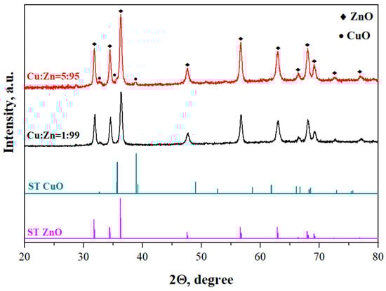
Figure 1.
X-ray images of CuO-ZnO films with Cu:Zn = 1:99 and 5:95 and standard sample from the database (curve ST ZnO and ST CuO).
The intensity of the wurtzite peaks is much more pronounced than that of the tenorite peaks. Furthermore, the intensity of the peaks increases as the copper concentration increases, which can be attributed to an improvement in the degree of crystallinity of the obtained materials. The dislocation density (δ) and strain (ε) and are listed in Table 1. Both parameters decrease, indicating a reduction in the number of defects occurring during film formation.

Table 1.
Measurement of dislocation density and strain of CuO-ZnO thin films.
3.2. SEM
According to SEM data, the surface of the film is solid and has a uniform distribution of well-formed crystallites (Figure 2). The average size of the crystallites is 18 nm. The film is composed of ZnO and CuO nanocrystallites that are evenly distributed throughout the film and are in contact with one another. This arrangement leads to the formation of n-p heterojunctions between the two oxides.
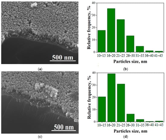
Figure 2.
SEM photos of surface (a,c), b distribution of nanocrystallites, (b,d) in Cu:Zn = 1:99 (a,b) and 5:95 (c,d).
3.3. Optical Properties
As can be seen from the calculations, CuO-ZnO thin films have a fairly high dislocation density, which indicates a high defect in the film structure. As a rule, films with such a structure have a complex type of optical absorption spectra, which is due to the existence of indirect interband transitions [14]. For them, the dependence of the absorption coefficient on the photon energy is more complex which, in general, can be described by the function
where α is the absorption coefficient; h is Planck’s constant; ν is the frequency of optical radiation; ∆Eg is the band gap; and Ep is the energy of a photon that is absorbed or emitted during indirect transitions.
α1/2 = f (hν), if ∆Eg − Ep < hν > ∆Eg + Ep
Using the technique described in [15], the band gap and indirect interband transitions were determined using optical absorption spectra (Figure 3).
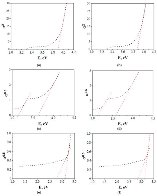
Figure 3.
Determination of the band gap (a,b) and indirect interband transitions (c–f) for materials 1CuO-99ZnO (a,c,e), 5CuO-95ZnO (b,d,f).
The band gap width Eg(α2) of 1CuO–99ZnO thin films is 3.90 eV, and 5CuO–95ZnO is 3.87 eV. This is significantly higher than that of pure ZnO obtained by the same technology, and equal to 3.26 eV [16]. The obtained Eg(α2) values are close to the band gap values of Co3O4-ZnO films obtained by us in [10]. An increase in the energy of direct transitions can occur as a result of the occupation of possible states in the conduction band by charge carriers [14]. It is evident from Figure 3a,b that it is also possible for there to be electron transition energies that are determined by film defects. Such transitions are determined by the Eg(α0.5) dependences, which are shown in Figure 3c–f. The transition energy equal to 3.65 eV for 1CuO-99ZnO and 3.58 eV for 5CuO-95ZnO is close to the band gap of copper-doped zinc oxide (Eg = 3.3–3.5 eV) [17]. It follows from the data in Figure 3c,d that transitions with lower energy are also present in the film. A more thorough analysis of this region (Figure 3e,f) showed that the energies are 2.78 and 3.13 eV for the 1CuO-99ZnO film; the energies are 2.87 and 3.13 eV for the 1CuO-99ZnO film. The found energy values of 2.78–2.81 eV correspond to the electron jump between the donor level of Cu2+ and the acceptor level of Cu+. And, the transition energy of 3.13 eV can correspond to transitions both between the acceptor level of Cu+ and the bottom of the conduction band, and between the vacancies of Zn and the top of the valence band [17].
Thus, the complex structure of the obtained films and the presence of copper (II) oxide crystallites actually leads to a narrowing of the forbidden band of the CuO-ZnO composite to 2.8 eV. As a consequence, the obtained materials will be sensitive not only to UV light, but also to visible radiation. This suggests that they can be used to create photosensitive sensors of the resistive type.
Author Contributions
Conceptualization, V.V.P. and E.M.B.; methodology, V.V.P. and E.M.B.; investigation, V.V.P. and I.O.I.; resources, V.V.P.; data curation, I.O.I.; writing—original draft preparation, I.O.I.; writing—review and editing, V.V.P. and E.M.B.; visualization, I.O.I.; funding acquisition, V.V.P. All authors have read and agreed to the published version of the manuscript.
Funding
This research was financially supported by the Russian Science Foundation 24-29-00203 Available on: https://rscf.ru/project/24-29-00203/ (accessed on 8 May 2025) at the Southern Federal University.
Institutional Review Board Statement
Not applicable.
Informed Consent Statement
Not applicable.
Data Availability Statement
The data presented in this study are available on request from the corresponding author.
Conflicts of Interest
The authors declare no conflicts of interest.
References
- Li, S.Q.; Yao, C.B.; Han, Y.; Jiang, G.Q.; Cai, Y.; Yin, H.T.; Sun, W.J. Synthesis, electrical and ultrafast nonlinear optical properties of Sn–ZnO composite film. Opt. Mater. 2019, 96, 109329. [Google Scholar] [CrossRef]
- Özgür, Ü.; Hofstetter, D.; Morkoc, H. ZnO devices and applications: A review of current status and future prospects. Proc. IEEE 2010, 98, 1255–1268. [Google Scholar] [CrossRef]
- Pillai, S.C.; Kelly, J.M.; Ramesh, R.; McCormack, D.E. Advances in the synthesis of ZnO nanomaterials for varistor devices. J. Mater. Chem. C 2013, 1, 3268–3281. [Google Scholar] [CrossRef]
- Wibowo, A.; Marsudi, M.A.; Amal, M.I.; Ananda, M.B.; Stephanie, R.; Ardy, H.; Diguna, L.J. ZnO nanostructured materials for emerging solar cell applications. RSC Adv. 2020, 10, 42838–42859. [Google Scholar] [CrossRef] [PubMed]
- Taabouche, A.; Bouabellou, A.; Kermiche, F.; Hanini, F.; Bouachiba, Y.; Kerdjac, T. Properties of cobalt-doped zinc oxide thin films grown by pulsed laser deposition on glass substrates. Mater. Sci. Semicond. Process. 2014, 28, 54–58. [Google Scholar] [CrossRef]
- Boukaous, C.; Benhaoua, B.; Telia, A.; Ghanem, S. Effect of copper doping sol-gel ZnO thin films: Physical properties and sensitivity to ethanol vapor. Mater. Res. Express 2017, 4, 105024. [Google Scholar] [CrossRef][Green Version]
- Sung, N.E.; Kang, S.W.; Shin, H.J.; Lee, H.K.; Lee, I.J. Cu doping effects on the electronic and optical properties of Cu-doped ZnO thin films fabricated by radio frequency sputtering. Thin Solid Film. 2013, 547, 285–288. [Google Scholar] [CrossRef]
- Muiva, C.M.; Sathiaraj, T.S.; Maabong, K. Effect of doping concentration on the properties of aluminium doped zinc oxide thin films prepared by spray pyrolysis for transparent electrode applications. Ceram. Int. 2011, 37, 555–560. [Google Scholar] [CrossRef]
- Rajan, A.; Arora, K.; Yadav, H.K.; Gupta, V.; Tomar, M. Copper doped ZnO thin film for ultraviolet photodetector with enhanced photosensitivity. MRS Online Proc. Libr. (OPL) 2013, 1494, 43–49. [Google Scholar] [CrossRef]
- Petrov, V.V.; Sysoev, V.V.; Ignatieva, I.O.; Gulyaeva, I.A.; Volkova, M.G.; Ivanishcheva, A.P.; Bayan, E.M. Nanocomposite Co3O4-ZnO thin films for photoconductivity sensors. Sensors 2023, 23, 5617. [Google Scholar] [CrossRef] [PubMed]
- Saini, M.; Singh, R.; Mitra, A.; Som, T. Photoresponse of pulsed laser deposited ZnO:Cu thin films. Sol. Energy 2020, 207, 228–234. [Google Scholar] [CrossRef]
- Petrov, V.V.; Ignatieva, I.O.; Volkova, M.G.; Gulyaeva, I.A.; Pankov, I.V.; Bayan, E.M. Polycrystalline transparent Al-doped ZnO thin films for photosensitivity and optoelectronic applications. Nanomaterials 2023, 13, 2348. [Google Scholar] [CrossRef] [PubMed]
- John, K.I.; Adenle, A.A.; Adeleye, A.T.; Onyia, I.P.; Amune-Matthews, C.; Omorogie, M.O. Unravelling the effect of crystal dislocation density and microstrain of titanium dioxide nanoparticles on tetracycline removal performance. Chem. Phys. Lett. 2021, 776, 138725. [Google Scholar] [CrossRef]
- Shalimova, K.V. Physics of Semiconductors, 2nd ed.; Energia: Moscow, Russia, 1976. [Google Scholar]
- Bayan, E.M.; Petrov, V.V.; Volkova, M.G.; Storozhenko, V.Y.; Chernyshev, A.V. SnO2–ZnO nanocomposite thin films: The influence of structure, composition and crystallinity on optical and electrophysical properties. J. Adv. Dielectr. 2021, 11, 2160008. [Google Scholar] [CrossRef]
- Ignatieva, I.O.; Volkova, M.G.; Gulyaeva, I.A.; Starnikova, A.P.; Petrov, V.V.; Bayan, E.M. The optical and electrophysical properties of Al-ZnO thin films. Mater. Today Proc. 2022, 52, 191–194. [Google Scholar] [CrossRef]
- Xu, C.X.; Sun, X.W.; Zhang, X.H.; Ke, L.; Chua, S.J. Photoluminescent properties of copper-doped zinc oxide nanowires. Nanotechnology 2004, 15, 856–861. [Google Scholar] [CrossRef]


Disclaimer/Publisher’s Note: The statements, opinions and data contained in all publications are solely those of the individual author(s) and contributor(s) and not of MDPI and/or the editor(s). MDPI and/or the editor(s) disclaim responsibility for any injury to people or property resulting from any ideas, methods, instructions or products referred to in the content. |
© 2025 by the authors. Licensee MDPI, Basel, Switzerland. This article is an open access article distributed under the terms and conditions of the Creative Commons Attribution (CC BY) license (https://creativecommons.org/licenses/by/4.0/).