1. Introduction
For decades, signal processing was performed with analog electronics, including during the era of analog computers, e.g., it used for solving differential equations. In the last five decades, most analog circuits were substituted with digital electronic systems. Artificial Neural Networks (ANNs) were originally inspired by analog systems, and implemented with analog electronics, but were limited to one perceptron. Today, they are computed by discretized digital computers. In this study, analog ANNs (AANNs) can be considered co-processors and investigated with respect to their digital counterparts.
The motivation of this study is manifold. Considering highly miniaturized and embedded sensor nodes based on digital silicon electronics (e.g., by using a microcontroller), which provide less than 20 kB RAM and integer arithmetic only, computations of ANNs are possible by transforming floating-point arithmetic models to scaled integer models without the loss of accuracy (details can be found in [
1]).
But from a resource point of view with respect to digital logic, the computation of a fully connected ANN with
N nodes and
L layers requires roughly estimated, assuming
N/
L nodes per layer, a data width of
W Bits (e.g., 8):
with T(S) as the transistor count for the storage of coefficients, T(AW) as the transistor count for one W-Bit adder and T(MW) for one W-Bit multiplier circuit, T(O) as the transistor count for the LUT storage to implement the (non-linear) transfer function. For W = 8 Bits. N = 9, and L = 3 we get a total count of about 44,000 transistors. An 8-Bit microcontroller (with a few kB of RAM and ROM, like the Atmel AVR 8 Bit) requires more than 100,000 transistors [
2].
A weighted analog electronics summation circuit, on the other hand, requires
l + 1 resistors and a difference amplifier with about 4–8 transistors (at least 2). An approximated non-linear transfer function, e.g., the sigmoid function, can be built from at least two transistors [
3], and typically less than twenty transistors [
4], if the gradient of the function is computed too. The hyperbolic tangents function can be implemented with only two diodes [
5]. Such small circuits are well suited for printed (organic) transistor electronics, replacing more and more silicon electronics, but they are still limiting circuits to a size of about 100 transistors and pose problems related to reduced stability, reproducibility, and statistical variance (of the entire circuit).
In our study, we address the following research questions to the computational ANN sub-domain:
Can an AANN be trained with a digital node graph and floating point arithmetic performing gradient-based error optimization and finally be converted to an analog circuit approximation (assuming there are ideal operational amplifiers)?
Can an AANN be trained with a digital node graph and floating point arithmetic performing gradient-based error optimization and finally be converted to an analog circuit approximation assuming there are non-ideal circuits, especially with tran-sistor-reduced circuits?
Are organic transistors suitable?
The implementation and approximation error of simple non-linear activation functions using transistor electronics are investigated and discussed here. Instead of using real analog electronics, we will substitute the circuits through a simulation model using the
spice3f simulator [
6], particularly the
ngspice version [
7]. We will consider different model abstraction levels, starting with an ideal operational amplifier (with voltage-controlled voltage sources), then, by using approximated real OPAMP models, and finally, by introducing transistor circuits with models of organic transistors [
8].
The next sections introduce the analog artificial neural network architecture and its electronic circuits with a short discussion of its limitations. A short introduction in the digital twin ANN is given with the modifications necessary for the digital analog transformation process. An experimental section follows which applies the proposed transformation process to the IRIS benchmark dataset. Finally, the results are discussed and the lessons learned are summarized.
2. Analog Neural Networks
With respect to analog computing, we have to distinguish and consider the following:
Different transistor technologies, e.g., Bipolar, JFET, OFET/OTFT, and OECT;
Operational amplifier (OPAMP) circuits with a minimal number of components (transistors);
Non-linear transfer functions, e.g., logistic regression (sigmoid) or hyperbolic tangents, and their implementation with a minimal number of components;
Transfer functions and the characteristic curves of OPAMP/sigmoid circuits;
A composed neuron (perceptron) circuit;
A full ANN.
We will start, for sake of simplicity, with traditional bipolar transistor circuits, as demonstrated in [
9], but limited to positive weights only. The minimum number of transistors for an OPAMP and the sigmoid function is three, without compromising usability, easy design procedure, and stability.
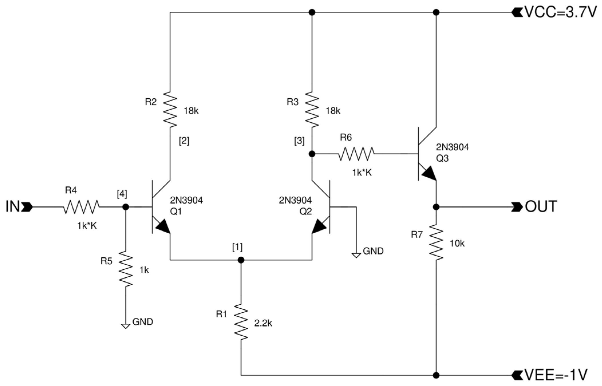
The circuit for a three-transistor OPAMP is shown in
Figure 1, posing a nearly linear transfer curve (with hard clipping), and a similar circuit for the smooth clipping non-linear sigmoid function implementation in
Figure 2. Both circuits are based on a differential NPN transistor pair, followed by a current and voltage amplifying PNP transistor or a current amplifying NPN transistor, respectively. To achieve an output voltage range of nearly [−10 V, 10 V], the power supply of the OPAMP3 circuit is set to [−10 V, 15 V].
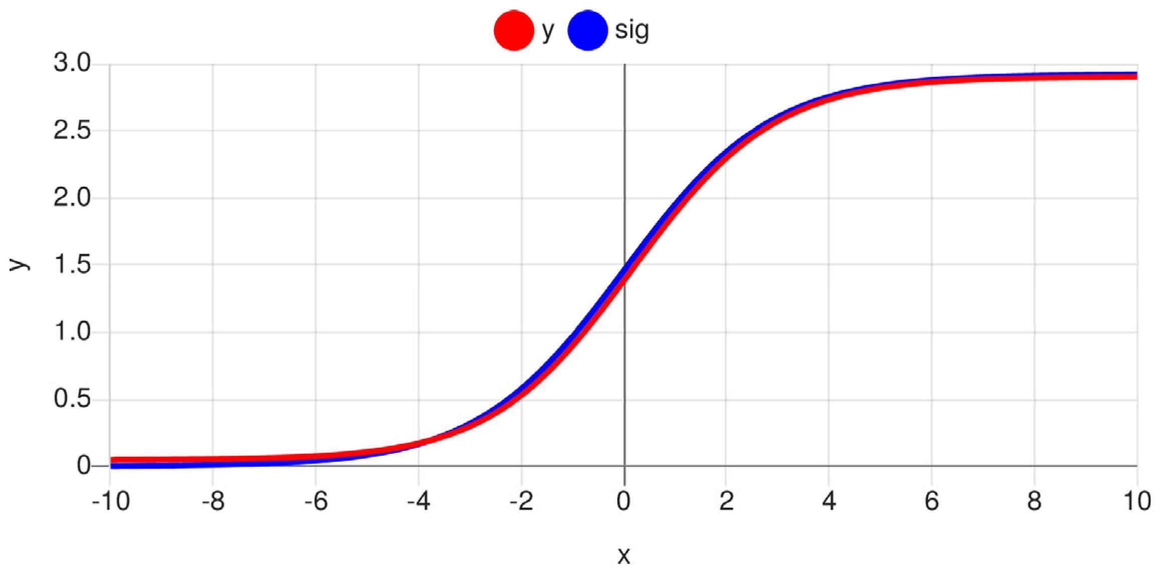
The sigmoid three-transistor circuit has different x- and y-scaling compared with the mathematical function [
10] but conforms with high accuracy to the scaled mathematical function, as shown in
Figure 3.
The x-scaling can be set by the input resistor multiplication factor k. The y-scale is always approximately in the value range [0.05 V, 2.9 V]. The SIGMOID3 circuit needs a slightly odd power supply [−1 V, 3.7 V].
Having defined the elementary cells OPAMP3 and SIGMOID3 of the neural network, we can compose neurons (one perceptron), the layers of the neurons, and the entire network. An ANN is described by the layer–network structure and parameters (weights, bias). The weights and bias values can be positive or negative. In principle, a common difference amplifier can be used. But, we will continuously have more than one negative and positive input, making the parametrization of such circuits difficult (the negative and positive gains cannot be indecently controlled). Therefore, we split the input path of a neuron into two paths, one for the negative weights and negative biases (if any exist), and one for the positive weights and biases (if any exist), finally, one merged by a unity gain difference amplifier. The entire architecture of a neuron is shown in
Figure 4.
Due to the current-controlled current-source model of a bipolar transistor and the current flows from the base to the emitter/collector, the gain of such a simplified OPAMP will be lower when compared with the gain of a mathematical ideal OPAMP. This gain mismatch (representing the weight of a neuron) requires a correction of the input resistor with a function depending on the original computed input resistor
ri value in relation to the feedback resistor
rf:
Additionally, there is a significant output offset of such a simplified OPAMP circuit (up to 3 V), which must be compensated for by feeding a compensation current flow via a resistor into the inverting input node. The offset voltage depends on the feedback resistor value and the accumulative (parallel) resistor of all the input resistors connected to the inverting input node. The dependency is extended if the non-inverting input is not grounded (as in the case of the difference amplifier, but fortunately, it has constant gain and resistor networks).
Assuming there is a fixed feedback resistor of the OPAMP
rf, e.g., 100 kΩ, an input resistor of the inverting OPAMP node is computed by the following:
3. Transformation Methods
An analog circuit is basically an undirected mesh graph of the current nodes, i.e., an electronic circuit has no real dedicated input and output ports. A digital feed-forward neural network, in contrast, is a directed graph of the functional nodes. There are basically two analog architectures which must be distinguished by a digital-to-analog transformation process:
Circuits with ideal OPAMPs and transfer functions (sigmoid), i.e., a theoretical and mathematical model of a neuron, which can use original ANN models and training methods and a direct digital-to-analog mapping model;
Circuits with non-ideal OPAMPs and transfer functions requiring modified models and training algorithms and an advanced digital-to-analog mapping model.
The first approach can be sub-divided into unconstrained ideal OPAMPs and nearly ideal but constrained real OPAMPs. An ideal OPAMP is characterized by an infinite open loop gain and infinite input and output value ranges. A real OPAMP has a finite high open loop gain (>100,000), but limited output value ranges, given by the supply voltages, e.g., [−10 V, 10 V]. The digital-to-analog transformation of ideal OPAMP circuits is trivial and not further considered in this study. The transformation of real OPAMP circuits or non-ideal OPAMP circuits is a challenge.
The challenges are as follows:
A limited open loop gain (50–100) can create a limit on the number of weights (<50);
The intermediate values can exceed the output range of the OPAMPs and clipping can occur;
The input and output ranges of non-linear transfer functions (e.g., sigmoid) are different from the mathematical versions;
Real OPAMP circuits create non-linearity (distortion) and highly relevant output offset voltages (Δ);
Composed circuits with bipolar transistors can cause complex side effects and a further deviation from an ideal OPAMP circuit due to the current-controlled current-source operational model of such transistors.
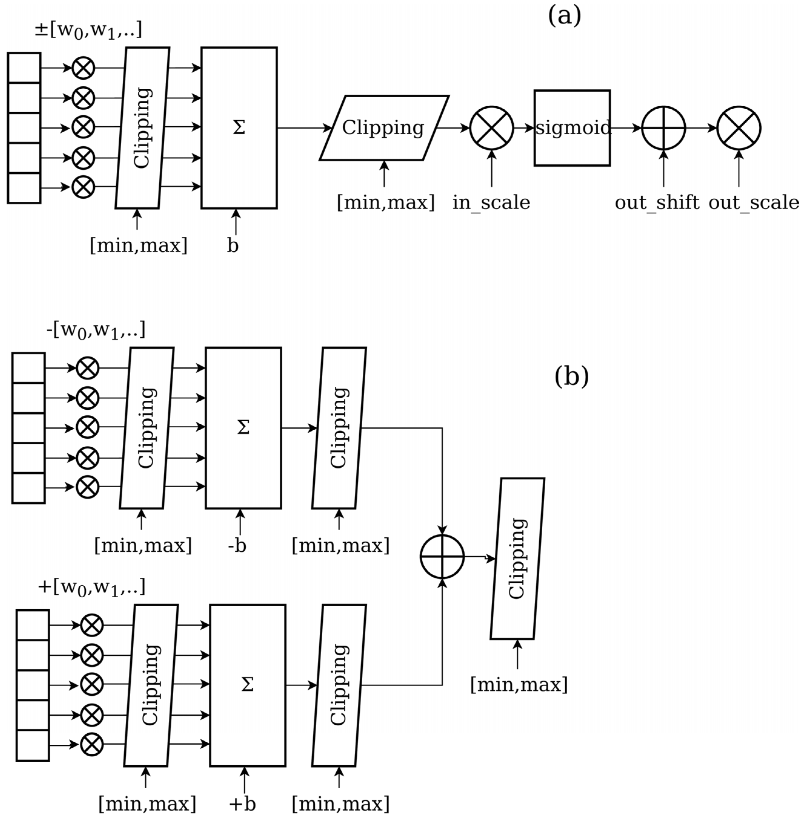
To reflect the limitations and deviation of reduced transistor circuits when compared with ideal OPAMP models, the neuron architecture in the digital model must be modified, as shown in
Figure 5. Additional clipping and scaling blocks are added to the weighted summation function and the non-linear sigmoid transfer function. Due to the limited open loop gain of the considered OPAMP3 circuit, weight parameter clipping is added too.
The ANN is trained with scaled and normalized data by using the digital modified network model and commonly available training algorithms, e.g., ADAM, SGD, and so on. The intermediate value and weight parameter clipping introduce distortion into the training process, but the results are commonly still presented with satisfying model parameter optimization and prediction error minimization. We assume a 1:1 digital–analog value mapping, i.e., a digital (mathematical) value of 1 corresponds to a voltage of 1 V.
The clipping parameters and the x-scaling of the transfer functions must be chosen carefully. In model architecture (a), even if there is an output clipping comparable to the electronic circuit behavior, there can be intermediate value overflows in one or both of the weight amplification branches. Higher mathematical values are not an issue for digital computations, but with 1:1 digital–analog mapping the absolute limits are given by the power supply voltages of the transistor circuits.
Therefore, the non-linear sigmoid function should be highly sensitive (i.e., low k values and high x-scaling). But the deviation of analog circuits like offset voltages can shift the transfer curve to their 0/1 boundaries resulting in saturated nodes that are not present in the digital model. A suitable compromise must be found on an iterative basis.
The analog sigmoid function has a fixed output value range of about [0 V, 3 V]. To reduce the risk of intermediate network values higher than the clipping range, the digital model is trained with a sigmoid value range [0, 1], finally reducing all the weights connected to the output of a sigmoid function by a factor of three.
We used the JavaScript ConvNetJS software framework ([
11], consisting of one file) to apply our modifications. ConvNetJS provides the advanced trainers and a broad range of network architectures, but is still very compact and easy to maintain. The main modification was the replacement of a commonly used practice to express the gradient function
g (of the transfer function
f) as a function of the original transfer function, e.g., in the case of the sigmoid function
y =
sigmoid(
x) this is
y(
y − 1), i.e., computing the gradients from the output values of
y. Instead, we modified the gradient computation by computing the gradient as a function of the input
x. Finally, we added the weight (filter) and output clipping.
The analog circuit is directly synthesized from the trained digital model. The synthesizer aanngen has to perform the following:
Net-list generation (spice);
Rescaling;
A resistor computation based on the weight and bias parameters under amplification correction and by connecting them to the appropriate sub-circuits (OPAMP3 OPN/OPP sub-circuits for the negative and positive weights/bias, respectively);
Adding and connecting sigmoid analog sub-circuits;
Adding offset correction resistors based on the computed circuit components.
The layer structure, weight, and bias parameters from the trained digital model are exported in JSON format and processed by the synthesizer program. Currently, the synthesizer creates an ngspice net-list with simulation control statements testing the analog circuit with test data.
4. Example: Benchmark IRIS Dataset Classification
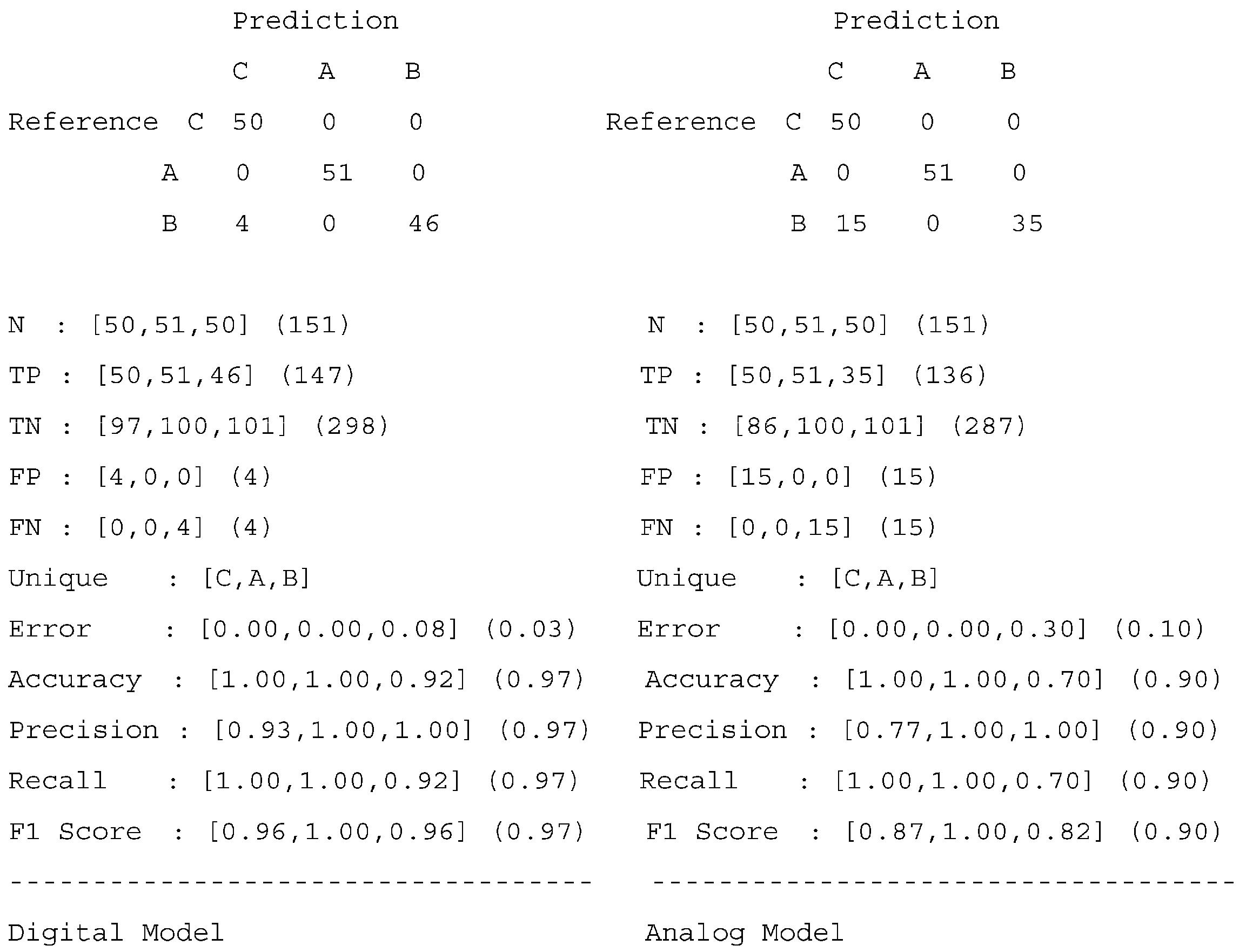
An ANN with a layered structure of [4, 3, 3] neurons and scaled sigmoid transfer functions was trained with the benchmark IRIS dataset consisting of 151 data instances. Because this study is only a proof of concept and comparison of a digital and an analog circuit model, the training and test were performed with the entire dataset.
The input vector x consists of four physical parameters (length, width, and petal length and width), which are normalized to the range [0, 1] independently, finally correlating to the analog voltage ranges [0 V, 1 V]. The three species classes are one-hot encoded (y). There is no soft-max layer at the output of the ANN model due to a lack of analog circuits implementing an interconnected multi-node function accurately. The first input layer is not present in the analog circuit (it is a pass-through layer).
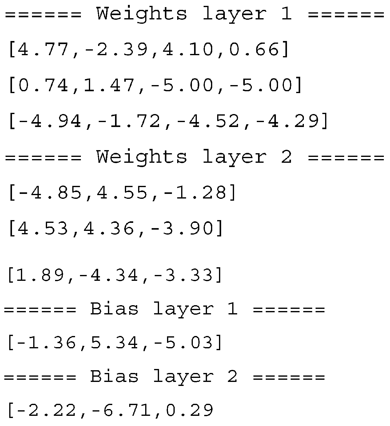
The training was performed with the ADAM optimize, α = 0.02, γ = 0.5, and a batch size of five. The filter clipping was set to five, the output scaling (of the summation function) was set to [−10, 10]. A typical model parameter set achieved after 10,000 single training iterations (by selecting the training instances randomly) is shown in
Figure 6. The classification results of the (clipped) digital model compared with the results from the analog circuit are shown in
Figure 7. The circuit was simulated by using
ngspice with altered settings to the input vector
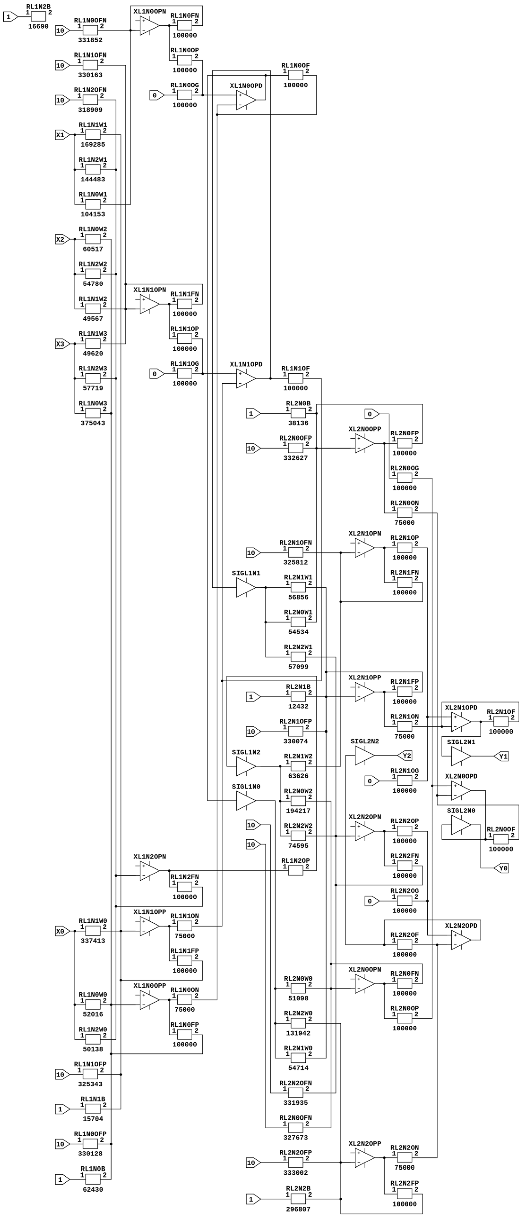
x. The generated resulting block architecture of the AANN is shown in
Figure A1 and the spice simulation model is shown
Figure A2 in
Appendix A.
The results show that the transformation process from a digital to an analog model succeeded. The average classification error increased (from 3% to 10%), but the overall accuracy of the analog model is still good and comparable to that of the digital model. Due to the limitations of the used simple and minimalistic circuits, the results are better than expected. The offsets and gain deviations were not fully compensated in the analog model.
5. Discussion
Due to the non-ideal analog circuit behavior when compared with the mathematical ideal operational amplifiers, there is increasing accumulative error with the increasing output deviation and prediction errors, finally reducing the safety margin in the classification. The non-ideal behavior is based on the following:
The output offset of the transistor circuits (OPAMP3) and the offset correction coefficient based on the resistor networks of the entire sub-circuit;
The lowered gain (which must be corrected) from the inverting input and gain correction coefficient depends on the resistor networks;
A limited gain due to the low open gain factor;
A drift due temperature variations;
Transistor parameter variations (e.g., hfe);
The deviation of the SIGMOID3 transfer curve from the mathematical (scaled) sigmoid function.
The y-scaling of the sigmoid is fixed, but the x-scaling can be freely chosen. A small x-scaling decreases the output values of the summation circuit, but increases its sensitivity to the offset errors. A larger x-scaling results in the opposite relationship.
The offsets and gain deviations were not fully compensated for in the analog model using the approximated and simplified calculation models derived from the simulation, but the analog model is still usable. But with an increasing number of layers (and neurons per layer), the value errors accumulate and can lower the model accuracy until it reaches the level of uselessness.
6. From Silicon to Organic Printed Electronics
The future goal of this study is to transform and implement digital computations in analog organic printed electronics. We can distinguish different organic transistor technologies:
Organic Thin-film Field-effect Transistors (OFET, OTFT) [
8];
Organic Electrochemical Transistors (OECT) [
12].
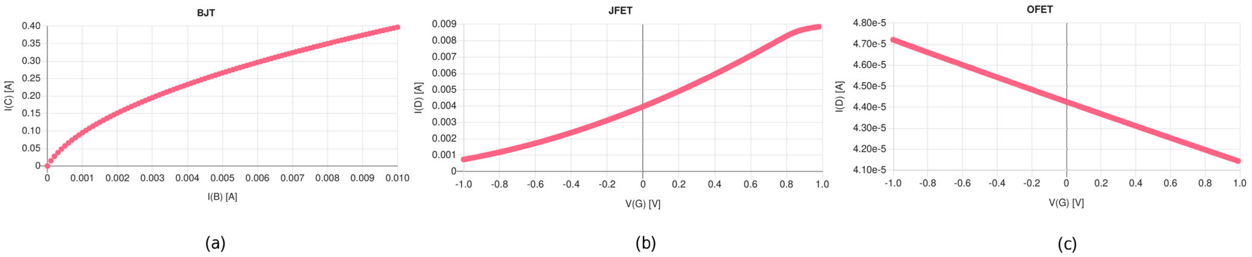
We started with silicon bipolar transistors to show the principal possibility to transform digital models to analog models. We were able to create neural circuits sufficiently close to the digital model’s behavior with a minimal number of transistors. The next step was the replacement of the BJT transistors with voltage-controlled JFET transistors and finally with OFET and OECT transistors. But some selected IV curve characteristics showed the next significant challenge. The JFTE and BCT curves are comparable with respect to steepness (gain) and the JFET circuits are well understood. The OFET curve (based on model from [
6]) shows a totally different behavior with respect to steepness and scale, as shown in
Figure 8. In [
10], the authors presented the idea that OECT transistors with a much more promising behavior are suitable to create our OPAMP3 and SIGMOID3 circuits.
Assuming a typical size of organic printed transistors of about 200 × 200 μm [
13], the circuit presented in this study with 66 transistors and 75 resistors would cover an area of about 2 × 2 mm, sufficiently small enough to be integrated into material-integrated sensor nodes [
14].
7. Conclusions
We could show that digital ANN models can be transformed into analog circuits with minimal transistor counts. The presented analog transistor circuits OPAMP3 and SIGMOID3 are elementary cells and the building blocks for neurons and neural networks. Each sub-circuit requires only 3 transistors. We tested and evaluated the approach with the IRIS benchmark dataset. We found that the digital model must be modified to reflect real circuit clipping (saturation) and a limited open loop gain (limiting the maximum weight values). The presented AANN example circuit consists of 16 OPAMP3 components and 6 SIGMOID3 components, in total 66 transistors and 75 resistors. Although the average classification error increased from 3 to 10%, the overall model accuracy is preserved.
To conclude, the digital-to-analog transformation of an ANN is possible, but the imperfections and correction of the simplified transistor circuits are limiting factors, especially for larger networks. We propose to use surrogate ML models of the sub-circuits for different parameter settings and the IO characteristics derived from and trained in simulations and integrated into the digital model training. This seems inevitable if OFET and OECT transistor technologies with much higher degrees of imperfection are used.


